


CY7C68013
9.0AC Electrical Characteristics
9.1USB Transceiver
USB 2.0-certified in fulland high-speed modes.
9.2Program Memory Read
|
tCL |
|
CLKOUT[10] |
|
|
|
tAV |
tAV |
A[15..0] |
|
|
|
tSTBL |
tSTBH |
PSEN# |
|
|
|
[11] |
tDH |
D[7..0] |
tACC1 |
data in |
|
|
|
|
tSOEL |
|
OE# |
|
|
|
tSCSL |
|
CS# |
|
|
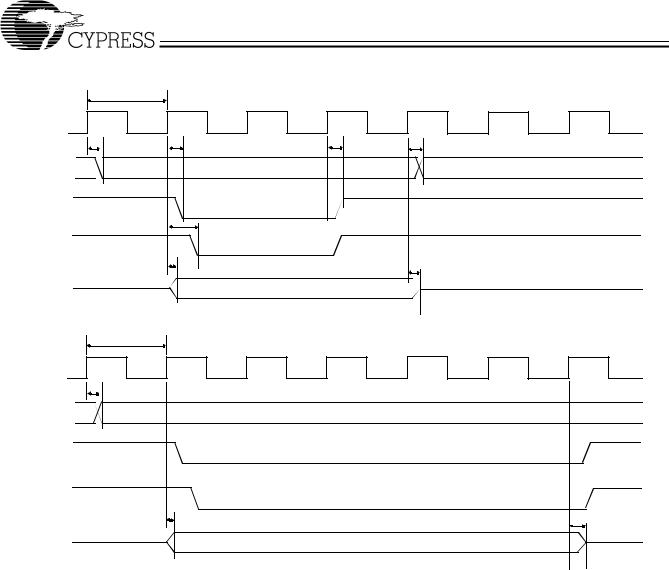
Figure 9-1. Program Memory Read Timing Diagram
Table 9-1. Program Memory Read Parameters
Parameter |
Description |
Min. |
Typ. |
Max. |
Unit |
Notes |
|
|
|
|
|
|
|
tCL |
1/CLKOUT Frequency |
|
20.83 |
|
ns |
48 MHz |
|
|
|
41.66 |
|
ns |
24 MHz |
|
|
|
|
|
|
|
|
|
|
83.2 |
|
ns |
12 MHz |
|
|
|
|
|
|
|
tAV |
Delay from Clock to Valid Address |
0 |
|
10.7 |
ns |
|
tSTBL |
Clock to PSEN Low |
0 |
|
8 |
ns |
|
tSTBH |
Clock to PSEN High |
0 |
|
8 |
ns |
|
tSOEL |
Clock to OE Low |
|
|
11.1 |
ns |
|
tSCSL |
Clock to CS Low |
|
|
13 |
ns |
|
tDSU |
Data Set-up to Clock |
9.6 |
|
|
ns |
|
tDH |
Data Hold Time |
0 |
|
|
ns |
|
Notes:
10.CLKOUT is shown with positive polarity.
11.tACC1 is computed from the above parameters as follows: tACC1(24 MHz) = 3*tCL – tAV –tDSU = 106 ns
tACC1(48 MHz) = 3*tCL – tAV – tDSU = 43 ns.
Document #: 38-08012 Rev. *F |
Page 30 of 48 |
CY7C68013
9.3Data Memory Read
tCL |
|
Stretch = 0 |
|
||
|
|
|
CLKOUT[10]
|
tAV |
|
tAV |
A[15..0] |
|
|
|
|
tSTBL |
|
tSTBH |
RD# |
|
|
|
|
tSCSL |
|
|
CS# |
|
|
|
OE# |
tSOEL |
|
|
|
|
|
|
|
[12] |
tDSU |
tDH |
D[7..0] |
tACC1 |
data in |
|
CLKOUT[10]
A[15..0]
RD#
CS#
D[7..0]
tCL |
Stretch = 1 |
|
|
|
|
tAV |
|
|
|
[12] |
tDSU |
|
tDH |
|
|
tACC1 |
|
|
|
data in |
Figure 9-2. Data Memory Read Timing Diagram
Parameter |
Description |
Min. |
Typ. |
Max. |
Unit |
Notes |
|
|
|
|
|
|
|
tCL |
1/CLKOUT Frequency |
|
20.83 |
|
ns |
48 MHz |
|
|
|
41.66 |
|
ns |
24 MHz |
|
|
|
|
|
|
|
|
|
|
83.2 |
|
ns |
12 MHz |
|
|
|
|
|
|
|
tAV |
Delay from Clock to Valid Address |
|
|
10.7 |
ns |
|
tSTBL |
Clock to RD LOW |
|
|
11 |
ns |
|
tSTBH |
Clock to RD HIGH |
|
|
11 |
ns |
|
tSCSL |
Clock to CS LOW |
|
|
13 |
ns |
|
tSOEL |
Clock to OE LOW |
|
|
11.1 |
ns |
|
tDSU |
Data Set-up to Clock |
9.6 |
|
|
ns |
|
tDH |
Data Hold Time |
0 |
|
|
ns |
|
When using the AUTPOPTR1 or AUTOPTR2 to address external memory, the address of AUTOPTR1 will only be active while either RD# or WR# are active. The address of AUTOPTR2 will be active throughout the cycle and meet the above address valid time for which is based on the stretch value.
Note:
12.tACC2 and tACC3 are computed from the above parameters as follows: tACC2(24 MHz) = 3*tCL – tAV –tDSU = 106 ns
tACC2(48 MHz) = 3*tCL – tAV – tDSU = 43 ns
tACC3(24 MHz) = 5*tCL – tAV –tDSU = 190 ns tACC3(48 MHz) = 5*tCL – tAV – tDSU = 86 ns.
Document #: 38-08012 Rev. *F |
Page 31 of 48 |
CY7C68013
9.4Data Memory Write
tCL
CLKOUT |
|
|
|
tAV |
tSTBL |
tSTBH |
tAV |
|
|||
A[15..0] |
|
|
|
WR# |
|
|
|
|
tSCSL |
|
|
CS# |
|
|
|
|
tON1 |
|
tOFF1 |
|
|
|
|
D[7..0] |
|
data out |
|
tCL |
|
Stretch = 1 |
|
|
|
|
|
CLKOUT |
|
|
|
|
tAV |
|
A[15..0] |
|
|
WR# |
|
|
CS# |
|
|
|
tON1 |
tOFF1 |
|
|
|
D[7..0] |
|
data out |
Figure 9-3. Data Memory Write Timing Diagram
Table 9-2. Data Memory Write Parameters
Parameter |
Description |
Min. |
Max. |
Unit |
Notes |
|
|
|
|
|
|
tAV |
Delay from Clock to Valid Address |
0 |
10.7 |
ns |
|
tSTBL |
Clock to WR Pulse LOW |
0 |
11.2 |
ns |
|
tSTBH |
Clock to WR Pulse HIGH |
0 |
11.2 |
ns |
|
tSCSL |
Clock to CS Pulse LOW |
|
13.0 |
ns |
|
tON1 |
Clock to Data Turn-on |
0 |
13.1 |
ns |
|
tOFF1 |
Clock to Data Hold Time |
0 |
13.1 |
ns |
|
When using the AUTPOPTR1 or AUTOPTR2 to address external memory, the address of AUTOPTR1 will only be active while either RD# or WR# are active. The address of AUTOPTR2 will be active throughout the cycle and meet the above address valid time for which is based on the stretch value.
Document #: 38-08012 Rev. *F |
Page 32 of 48 |
CY7C68013
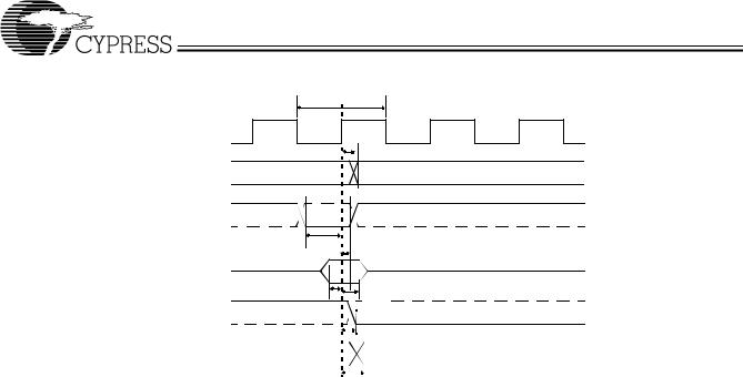
9.5GPIF Synchronous Signals
|
tIFCLK |
IFCLK |
|
|
tSGA |
GPIFADR[8:0] |
|
RDYX |
|
tSRY |
|
|
tRYH |
DATA(input) |
valid |
|
|
tSGD |
t |
|
DAH |
CTLX |
|
|
|
tXCTL |
|
|
|
|
|
|
|
|
|
|
|||
|
|
|
|
|
|
|
|
|
|
|
|||||
|
DATA(output) |
N |
|
N+1 |
|
|
|
||||||||
|
|
|
|
|
|
|
|||||||||
|
|
|
|
|
|
|
|
|
|
|
|
|
|
|
|
|
|
|
tXGD |
|
|
|
|
|
|
|
|
|
|||
|
|
|
|
|
|
|
|
|
|
|
|
|
|
||
|
Figure 9-4. GPIF Synchronous Signals Timing Diagram[13] |
|
|
|
|||||||||||
Table 9-3. GPIF Synchronous Signals Parameters with Internally Sourced IFCLK[14, 15] |
|
|
|
||||||||||||
Parameter |
|
Description |
|
Min. |
|
Max. |
Unit |
||||||||
|
|
|
|
|
|
|
|
|
|
|
|
|
|
|
|
tIFCLK |
IFCLK Period |
|
|
|
|
|
|
|
|
20.83 |
|
|
|
ns |
|
tSRY |
RDYX to Clock Set-up Time |
|
|
|
|
|
|
|
|
8.9 |
|
|
|
ns |
|
tRYH |
Clock to RDYX |
|
|
|
|
|
|
|
|
0 |
|
|
|
ns |
|
tSGD |
GPIF Data to Clock Set-up Time |
|
|
|
|
|
|
|
|
9.2 |
|
|
|
ns |
|
tDAH |
GPIF Data Hold Time |
|
|
|
|
|
|
|
|
0 |
|
|
|
ns |
|
tSGA |
Clock to GPIF Address Propagation Delay |
|
|
|
7.5 |
ns |
|||||||||
tXGD |
Clock to GPIF Data Output Propagation Delay |
|
|
|
11 |
ns |
|||||||||
tXCTL |
Clock to CTLX Output Propagation Delay |
|
|
|
6.7 |
ns |
|||||||||
Table 9-4. GPIF Synchronous Signals Parameters with Externally Sourced IFCLK[15] |
|
|
|
||||||||||||
Parameter |
|
Description |
|
Min. |
|
Max. |
Unit |
||||||||
|
|
|
|
|
|
|
|
|
|
|
|
|
|
||
tIFCLK |
IFCLK Period |
|
|
|
|
|
|
|
|
20.83 |
|
200 |
ns |
||
tSRY |
RDYX to Clock Set-up Time |
|
|
|
|
|
|
|
|
2.9 |
|
|
|
ns |
|
tRYH |
Clock to RDYX |
|
|
|
|
|
|
|
|
3.7 |
|
|
|
ns |
|
tSGD |
GPIF Data to Clock Set-up Time |
|
|
|
|
|
|
|
|
3.2 |
|
|
|
ns |
|
tDAH |
GPIF Data Hold Time |
|
|
|
|
|
|
|
|
4.5 |
|
|
|
ns |
|
tSGA |
Clock to GPIF Address Propagation Delay |
|
|
|
11.5 |
ns |
|||||||||
tXGD |
Clock to GPIF Data Output Propagation Delay |
|
|
|
15 |
ns |
|||||||||
tXCTL |
Clock to CTLX Output Propagation Delay |
|
|
|
10.7 |
ns |
|||||||||
Notes:
13.Dashed lines denote signals with programmable polarity.
14.GPIF asynchronous RDYx signals have a minimum set-up time of 50 ns when using internal 48-MHz IFCLK.
15.IFCLK must not exceed 48 MHz.
Document #: 38-08012 Rev. *F |
Page 33 of 48 |