

AD8531/AD8532/AD8534
APPLICATIONS
HIGH OUTPUT CURRENT, BUFFERED
REFERENCE/REGULATOR
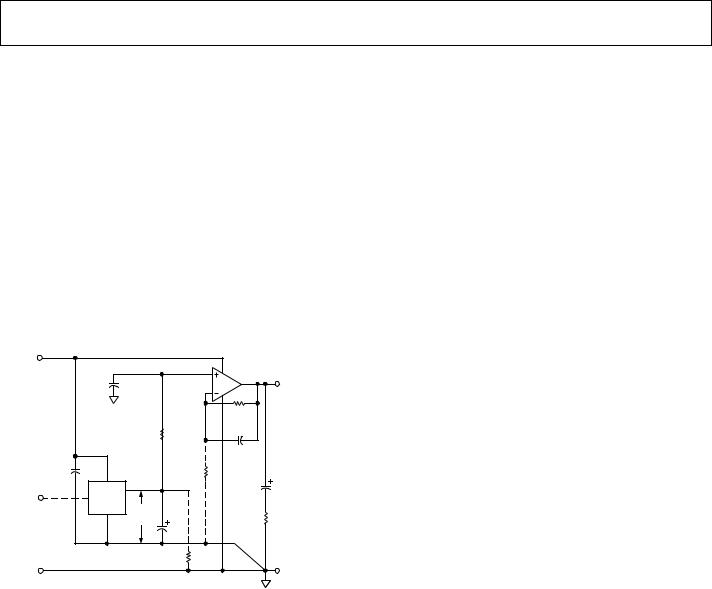
Many applications require stable voltage outputs relatively close in potential to an unregulated input source. This low dropout type of reference/regulator is readily implemented with a rail- to-rail output op amp, and is particularly useful when using a higher current device such as the AD8531/AD8532/AD8534. A typical example is the 3.3 V or 4.5 V reference voltage developed from a 5 V system source. Generating these voltages requires a three terminal reference, such as the REF196 (3.3 V) or the REF194 (4.5 V), both of which feature low power, with sourcing outputs of 30 mA or less. Figure 42 shows how such a reference can be outfitted with an AD8531/AD8532/AD8534 buffer for higher currents and/or voltage levels, plus sink and source load capability.
VS |
|
|
|
U2 |
|
5V |
|
|
|
|
|
|
C1 |
|
|
AD8531 |
|
|
|
|
VOUT1 = |
|
|
0.1µF |
|
|
3.3V @ 100mA |
|
|
|
|
|
|
|
|
|
|
|
|
R2 |
|
|
|
|
R1 |
10kΩ 1% |
|
|
|
|
10kΩ |
|
|
|
|
|
1% |
C2 |
|
|
|
|
|
|
|
C3 |
|
|
R3 |
0.1µF |
|
2 |
|
|
|
||
0.1µF |
|
(SeeText) |
C5 |
|
|
3 |
U1 |
6 |
|
100µF/16V |
|
|
|
TANTALUM |
|
||
VC |
REF196 |
VOUT2 = |
|
|
|
ON/OFF |
|
|
R5 |
|
|
CONTROL |
4 |
3.3V |
|
|
|
C4 |
0.2Ω |
|
|||
INPUT CMOS HI |
|
|
|||
|
|
1µF |
|
|
|
(OR OPEN) = ON |
|
|
|
|
|
|
|
|
|
|
|
LO = OFF |
|
|
R4 |
|
|
|
|
|
|
|
|
VS |
|
|
3.3kΩ |
VOUT |
-042 |
|
|
|
|||
COMMON |
|
|
|
COMMON |
01099 |
|
|
|
|
|
|
Figure 42. A High Output Current Reference/Regulator
The low dropout performance of this circuit is provided by stage U2, an AD8531 connected as a follower/buffer for the basic reference voltage produced by U1. The low voltage saturation characteristic of the AD8531/AD8532/AD8534 allows up to 100 mA of load current in the illustrated use, as a 5 V to 3.3 V converter with good dc accuracy. In fact, the
dc output voltage change for a 100 mA load current delta measured less than 1 mV. This corresponds to an equivalent output impedance of < 0.01 Ω. In this application, the stable 3.3 V from U1 is applied to U2 through a noise filter, R1–C1. U2 replicates the U1 voltage within a few millivolts, but at a higher current output at VOUT1, with the ability to both sink and source output current(s), unlike most IC references. R2 and C2 in the feedback path of U2 provide additional noise filtering.
Transient performance of the reference/regulator for a 100 mA step change in load current is also quite good and is largely determined by the R5 to C5 output network. With values as shown, the transient is about 20 mV peak and settles to within 2 mV in less than 10 µs for either
polarity. Although room exists for optimizing the transient response, any changes to the R5 to C5 network should be verified by experiment to preclude the possibility of excessive ringing with some capacitor types.
To scale VOUT2 to another (higher) output level, the optional resistor R3 (shown dotted) is added, causing, the new VOUT1 to become
|
|
|
|
R2 |
|
V |
=V |
× 1 |
+ |
|
|
|
|||||
OUT1 |
OUT2 |
|
|
R3 |
|
The circuit can either be used as shown, as a 5 V to 3.3 V reference/regulator, or with ON/OFF control. By driving Pin 3 of U1 with a logic control signal as noted, the output is switched ON/OFF. Note that when ON/OFF control is used, resistor R4 must be used with U1 to speed ON-OFF switching.
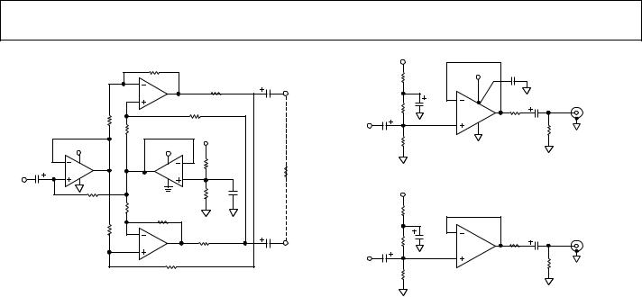
SINGLE-SUPPLY, BALANCED LINE DRIVER
The circuit in Figure 43 is a unique line driver circuit topology used in professional audio applications. It has been modified for automotive and multimedia audio applications. On a single 5 V supply, the line driver exhibits less than 0.7% distortion into a 600 Ω load from 20 Hz to 15 kHz (not shown) with an input signal level of 4 V p-p. In fact, the output drive capability of the AD8531/AD8532/AD8534 maintains this level for loads as small as 32 Ω. For input signals less than 1 V p-p, the THD is less than 0.1%, regardless of load. The design is a transformerless, balanced transmission system where output commonmode rejection of noise is of paramount importance. As with the transformer-based system, either output can be shorted
to ground for unbalanced line driver applications without changing the circuit gain of 1. Other circuit gains can be set according to the equation in the diagram. This allows the design to be easily configured for inverting, noninverting, or differential operation.
Rev. E | Page 15 of 20
AD8531/AD8532/AD8534 |
|
|
|
|||||
|
|
|
|
R3 |
|
|
|
|
|
|
|
|
10kΩ |
|
|
C3 |
|
|
|
|
2 |
|
|
|
R5 |
|
|
|
|
|
|
|
47µF |
||
|
|
|
|
A2 |
1 |
50Ω |
VO1 |
|
|
|
|
3 |
|
|
|||
|
|
|
|
R6 |
|
|||
|
|
|
|
|
|
|
|
|
|
|
R2 |
|
|
|
10kΩ |
|
|
|
|
R7 |
|
|
|
|
|
|
|
|
10kΩ |
|
|
|
|
|
|
|
|
|
10kΩ |
|
5V |
|
|
|
|
5V |
|
|
|
|
|
|
|
|
|
|
|
12V |
|
|
|
|
C1 |
2 |
1 |
|
7 |
|
6 |
R8 |
RL |
22µF |
3 A1 |
|
A1 |
5 |
100kΩ |
|||
VIN |
|
|
|
|
600Ω |
|||
|
|
|
|
|
R9 |
C2 |
|
|
|
|
R1 |
R11 |
R12 |
100kΩ |
1µF |
|
|
|
|
|
|
|
||||
|
|
10kΩ |
|
|
|
|
||
A1, A2 = 1/2 AD8532 |
10kΩ 10kΩ |
|
|
C4 |
||||
R10 |
6 |
|
|
R14 |
|
|||
GAIN =R3 |
|
10kΩ |
|
|
|
47µF |
||
|
|
|
7 |
50Ω |
||||
|
|
|
A2 |
VO2 |
||||
R2 |
|
|
5 |
R13 |
|
|
||
SET: R7, R10, R11 = R2 |
|
|
|
-043 |
||||
|
|
10kΩ |
|
|
||||
SET: R6, R12, R13 = R3 |
|
|
|
|
|
01099 |
||
|
|
|
|
|
|
|||
Figure 43. A Single-Supply, Balanced Line Driver for Multimedia and Automotive Applications
SINGLE-SUPPLY HEADPHONE AMPLIFIER
Because of its speed and large output drive, the AD8531/ AD8532/AD8534 make an excellent headphone driver, as illustrated in Figure 44. Its low supply operation and rail-to-rail inputs and outputs give a maximum signal swing on a single
5 V supply. To ensure maximum signal swing available to drive the headphone, the amplifier inputs are biased to V+/2, which in this case is 2.5 V. The 100 kΩ resistor to the positive supply is equally split into two 50 kΩ resistors, with their common point bypassed by 10 µF to prevent power supply noise from contaminating the audio signal.
The audio signal is then ac-coupled to each input through a 10 µF capacitor. A large value is needed to ensure that the 20 Hz audio information is not blocked. If the input already has the proper dc bias, the ac coupling and biasing resistors are not required. A 270 µF capacitor is used at the output to couple the amplifier to the headphone. This value is much
larger than that used for the input because of the low impedance of the headphones, which can range from 32 Ω to 600 Ω. An additional 16 Ω resistor is used in series with the output capacitor to protect the output stage of the op amp by limiting capacitor discharge current. When driving a 48 Ω load, the circuit exhibits less than 0.3% THD+N at output drive levels of 4 V p-p.
V 5V |
|
|
|
|
50kΩ |
|
V 5V |
1µF/0.1µF |
|
|
|
|
|
|
50kΩ |
10µF |
1/2 |
16Ω 270µF |
LEFT |
|
|
AD8532 |
|
HEADPHONE |
LEFT |
|
50kΩ |
INPUT |
10µF |
|
|
100kΩ |
|
|
|
|
V |
|
|
|
|
50kΩ |
|
|
|
|
|
50kΩ |
10µF |
1/2 |
16Ω |
270µF |
RIGHT |
|
|
AD8532 |
|
|
HEADPHONE |
RIGHT |
|
|
INPUT |
10µF |
50kΩ |
|
100kΩ |
|
|
|
|
|
|
01099044- |
Figure 44. A Single-Supply, Stereo Headphone Driver
SINGLE-SUPPLY, TWO-WAY LOUDSPEAKER CROSSOVER NETWORK
Active filters are useful in loudspeaker crossover networks for reasons of small size, relative freedom from parasitic effects, the ease of controlling low/high channel drive, and the controlled driver damping provided by a dedicated amplifier. Both SallenKey (SK) and multiple-feedback (MFB) filter architectures are useful in implementing active crossover networks. The circuit shown in Figure 45 is a single-supply, two-way active crossover that combines the advantages of both filter topologies. This active crossover exhibits less than 0.4% THD+N at output levels of 1.4 V rms using general purpose unity-gain HP/LP stages.
In this two-way example, the LO signal is a dc-500 Hz LP woofer output, and the HI signal is the HP (>500 Hz) tweeter output. U1B forms an LP section at 500 Hz, while U1A provides an HP section, covering frequencies ≥500 Hz.
Rev. E | Page 16 of 20
AD8531/AD8532/AD8534
|
C1 |
R1 |
|
R3 |
|
500Hz |
|
0.01µF |
|
270µF |
AND UP |
||
|
31.6kΩ |
|
49.9Ω |
|||
|
|
|
|
|
+ |
HI |
|
|
|
|
VS |
|
|
|
|
C2 |
|
|
|
|
|
|
|
U1A |
|
100kΩ |
|
|
|
0.01µF |
|
|
||
|
|
|
3 |
AD8532 |
|
|
VIN |
|
|
1 |
|
|
|
|
|
2 |
|
|
||
RIN |
R2 |
|
|
|
|
|
|
|
4 |
|
|
||
100kΩ |
31.6kΩ |
|
|
|
|
|
CIN |
R5 |
R6 |
|
R4 |
|
DC – |
10µF |
|
270µF |
500Hz |
|||
31.6kΩ |
31.6kΩ |
|
49.9Ω |
|||
|
|
|
||||
|
|
|
|
|
+ |
LO |
|
|
|
|
C3 |
|
|
|
|
R7 |
|
|
|
|
|
VS |
15.8kΩ |
|
0.01µF |
|
100kΩ |
|
|
|
|
|
|
|
100kΩ |
C4 |
6 |
7 |
|
|
|
0.02µF |
5 |
|
|
|||
|
|
|
U1B |
|
|
|
100kΩ |
|
|
|
|
||
10µF |
|
AD8532 |
|
|
||
VS |
|
5V |
|
|
|
|
0.1µF |
100µF/25V |
|
|
|
01099-045 |
|
TO U1 |
|
COM |
|
|
|
|
|
|
|
|
|
|
|
Figure 45. A Single-Supply, Two-Way Active Crossover
The crossover example frequency of 500 Hz can be shifted lower or higher by frequency scaling of either resistors or capacitors. In configuring the circuit for other frequencies, complementary LP/HP action must be maintained between sections, and component values within the sections must be in the same ratio. Table 6 provides a design aid to adaptation, with suggested standard component values for other frequencies.
For additional information on the active filters and active crossover networks, please consult the data sheet for the OP279, a dual rail-to-rail high output current operational amplifier.
Table 6. RC Component Selection for Various Crossover Frequencies1
Crossover Frequency (Hz) |
R1/C1 (U1A)2 R5/C3 (U1B)3 |
100 |
160 kΩ/0.01 µF |
200 |
80.6 kΩ/0.01 µF |
319 |
49.9 kΩ/0.01 µF |
500 |
31.6 kΩ/0.01 µF |
1 k |
16 kΩ/0.01 µF |
2 k |
8.06 kΩ/0.01 µF |
5 k |
3.16 kΩ/0.01 µF |
10 k |
1.6 kΩ/0.01 µF |
|
|
1 Applicable for filter a = 2.
2 For Sallen-Key stage U1A: R1 = R2, and C1 = C2, and so on.
3 For multiple feedback stage U1B: R6 = R5, R7 = R5/2, and C4 = 2C3.
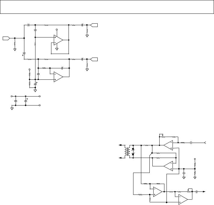
DIRECT ACCESS ARRANGEMENT FOR TELEPHONE LINE INTERFACE
Figure 46 illustrates a 5 V only transmit/receive telephone line interface for 600 Ω transmission systems. It allows full duplex transmission of signals on a transformer coupled 600 Ω line in a differential manner. Amplifier A1 provides gain that can be adjusted to meet the modem output drive requirements. Both A1 and A2 are configured to apply the largest possible signal on a single supply to the transformer. Because of the high output current drive and low dropout voltage of the
AD8531/AD8532/AD8534, the largest signal available on a single 5 V supply is approximately 4.5 V p-p into a 600 Ω transmission system. Amplifier A3 is configured as a difference amplifier for two reasons: (1) It prevents the transmit signal from interfering with the receive signal, and (2) it extracts the receive signal from the transmission line for amplification by A4. A4’s gain can be adjusted in the same manner as that of A1 to meet the modem’s input signal requirements. Standard resistor values permit the use of SIP (single in-line package) format resistor arrays.
|
|
|
|
P1 |
|
|
|
|
|
|
|
|
|
|
|
|
|
Tx GAIN |
|
|
|
|
|
|
|
|
|
|
|
|
|
ADJUST |
R2 |
|
|
|
|
|
|
||
|
|
|
|
|
|
9.09kΩ |
R1 |
|
C1 |
|
TRANSMIT |
||
TO TELEPHONE |
|
|
|
|
|
|
|
|
|
|
|||
|
R3 |
|
|
2kΩ |
|
|
|
|
0.1µF |
||||
|
|
|
|
2 |
|
10kΩ |
TxA |
||||||
LINE |
|
360Ω |
|
|
1 |
|
|
|
|
|
|
|
|
1:1 |
|
|
|
A1 |
|
|
|
|
|
|
|
||
|
|
|
R5 |
3 |
|
|
|
|
|
|
|||
|
6.2V |
|
|
|
|
|
|
|
|
|
|
||
ZO |
|
|
|
|
|
|
|
|
|
|
|
||
|
|
10kΩ |
|
|
|
|
|
|
|
|
|
||
600Ω |
6.2V |
|
|
|
|
|
|
|
|
|
|
|
|
|
|
|
|
|
|
|
|
|
|
5V DC |
|||
T1 |
|
|
|
|
|
|
|
|
|
|
|||
|
|
|
R6 |
|
|
6 |
|
|
|
|
|
|
|
MIDCOM |
|
|
|
|
|
|
|
|
|
|
|
||
|
|
|
10kΩ 7 |
|
|
|
|
|
|
R7 |
|||
671-8005 |
|
|
|
A2 |
5 |
|
|
|
|
|
|||
|
|
|
|
|
|
|
|
|
|
|
10kΩ |
||
|
|
|
|
|
|
|
|
|
|
|
10µF |
|
R8 |
|
|
|
|
|
|
|
|
|
|
|
|
10kΩ |
|
|
|
|
|
|
|
|
|
|
|
|
|
|
|
|
|
R9 |
|
R10 |
|
|
|
|
|
|
|
|
|
|
|
10kΩ |
|
10kΩ |
|
|
|
|
|
|
P2 |
|
|
|
|
|
|
|
|
|
|
|
|
Rx GAIN |
|
||
|
|
|
2 |
|
|
R13 |
|
R14 |
ADJUST |
RECEIVE |
|||
|
R11 |
|
A3 |
1 |
10kΩ 14.3kΩ |
|
|
|
RxA |
||||
|
10kΩ |
3 |
|
|
|
6 |
|
|
2kΩ |
|
C2 |
||
|
|
R12 |
|
|
|
|
|
|
|
|
|||
|
|
|
|
|
|
|
|
A4 |
|
7 |
0.1µF |
||
A1, A2 = 1/2 AD8532 |
10kΩ |
|
|
|
|
|
5 |
|
|
|
01099046- |
||
|
|
|
|
|
|
|
|
|
|||||
A3, A4 = 1/2 AD8532 |
|
|
|
|
|
|
|
|
|
|
|
||
Figure 46. A Single-Supply Direct Access Arrangement for Modems
Rev. E | Page 17 of 20