

THEORY OF OPERATION
The AD8531/AD8532/AD8534 are all CMOS, high output current drive, rail-to-rail input/output operational amplifiers. Their high output current drive and stability with heavy capacitive loads make the AD8531/AD8532/AD8534 excellent choices as drive amplifiers for LCD panels.
Figure 36 illustrates a simplified equivalent circuit for the AD8531/AD8532/AD8534. Like many rail-to-rail input amplifier configurations, it comprises two differential pairs, one N-channel (M1 to M2) and one P-channel (M3 to M4). These differential pairs are biased by 50 µA current sources, each with a compliance limit of approximately 0.5 V from either supply voltage rail. The differential input voltage is then converted into a pair of differential output currents. These differential output currents are then combined in a compound folded-cascade second gain stage (M5 to M9). The outputs of the second gain stage at M8 and M9 provide the gate voltage drive to the rail-to- rail output stage. Additional signal current recombination for the output stage is achieved through the use of Transistor M11 to Transistor M14.
To achieve rail-to-rail output swings, the AD8531/AD8532/ AD8534 design employs a complementary, common source output stage (M15–M16). However, the output voltage swing is directly dependent on the load current, as the difference between the output voltage and the supply is determined by the AD8531/AD8532/AD8534’s output transistors on channel resistance (see Figure 12 and Figure 13). The output stage also exhibits voltage gain by virtue of the use of common source amplifiers; as a result, the voltage gain of the output stage (thus, the open-loop gain of the device) exhibits a strong dependence to the total load resistance at the output of the AD8531/AD8532/AD8534.
|
|
V+ |
|
50µA |
100µA |
100µA |
20µA |
|
|
|
M11 |
|
|
|
M5 |
|
M12 |
|
|
|
VB2 |
M8 |
|
M1 |
M3 |
M4 |
M2 |
|
M15 |
IN– |
|
|
|
|
OUT |
|
|
|
|
|
|
IN+ |
|
|
M6 |
|
M16 |
|
|
VB3 |
M9 |
M14 |
|
|
|
|
|
|
20µA |
|
|
50µA |
M7 |
M10 |
M13 |
|
01099-036 |
||||
|
|
V– |
||
|
|
|
Figure 36. AD8531/AD8532/AD8534 Simplified Equivalent Circuit
AD8531/AD8532/AD8534
SHORT-CIRCUIT PROTECTION
As a result of the design of the output stage for maximum load current capability, the AD8531/AD8532/AD8534 do not have any internal short-circuit protection circuitry. Direct connection of the output of the AD8531/AD8532/AD8534 to the positive supply in single-supply applications destroys the device. In those applications where some protection is needed, but not at the expense of reduced output voltage headroom, a low value resistor in series with the output, as shown in Figure 37, can be used. The resistor, connected within the feedback loop of the amplifier, has very little effect on the
performance of the amplifier other than limiting the maximum available output voltage swing. For single 5 V supply applications, resistors less than 20 Ω are not recommended.
5V
VIN |
RX |
AD8532 |
20Ω |
VOUT |
01099-037
Figure 37. Output Short-Circuit Protection
POWER DISSIPATION
Although the AD8531/AD8532/AD8534 are capable of providing load currents to 250 mA, the usable output load current drive capability is limited to the maximum power dissipation allowed by the device package used. In any application, the absolute maximum junction temperature for the AD8531/AD8532/AD8534 is 150°C. The maximum junction temperature should never be exceeded because the device could suffer premature failure. Accurately measuring power dissipation of an integrated circuit is not always a straightforward exercise, so Figure 38 has been provided as a design aid for either setting a safe output current drive level or selecting a heat sink for the package options available on the AD8531/AD8532/AD8534.
Rev. E | Page 11 of 20
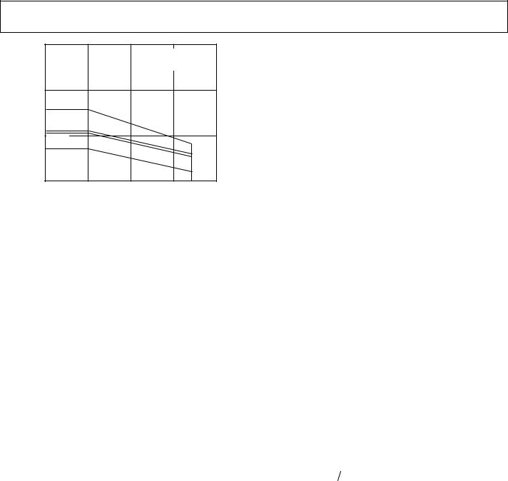
AD8531/AD8532/AD8534
1.5
TJ MAX = 150°C
FREE AIR
NO HEAT SINK
(W) |
1.0 |
|
|
|
|
|
DISSIPATION |
SOIC |
|
|
|
|
|
|
|
|
|
|
||
|
θJA = 158°C/W |
|
|
|
|
|
|
TSSOP |
|
|
|
|
|
|
θJA = 240°C/W |
|
|
|
|
|
POWER |
|
|
|
|
|
|
0.5 |
SOT-23 |
|
|
|
|
|
|
θJA = 236°C/W |
|
|
|
|
|
|
|
SC70 |
|
|
|
|
|
|
θJA = 376°C/W |
|
|
|
01099-038 |
|
0 |
|
|
|
|
|
|
0 |
25 |
50 |
75 |
85 |
100 |
|
|
|
TEMPERATURE (°C) |
|
|
|
Figure 38. Maximum Power Dissipation vs. Ambient Temperature
These thermal resistance curves were determined using the AD8531/AD8532/AD8534 thermal resistance data for each package and a maximum junction temperature of 150°C.
The following formula can be used to calculate the internal junction temperature of the AD8531/AD8532/AD8534 for any application:
TJ = PDISS ×θJA +TA
where:
TJ is the junction temperature.
PDISS is the power dissipation.
θJA is the package thermal resistance, junction-to-case.
TA is the ambient temperature of the circuit.
To calculate the power dissipated by the AD8531/AD8532/AD8534, the following equation can be used:
PDISS = ILOAD ×(VS −VOUT )
where:
ILOAD is the output load current.
VS is the supply voltage.
VOUT is the output voltage.
The quantity within the parentheses is the maximum voltage developed across either output transistor. As an additional design aid in calculating available load current from the AD8531/AD8532/AD8534, Figure 5 illustrates the output voltage of the AD8531/AD8532/AD8534 as a function of load resistance.
POWER CALCULATIONS FOR VARYING OR UNKNOWN LOADS
Often, calculating power dissipated by an integrated circuit to determine if the device is being operated in a safe range is not as simple as it might seem. In many cases power cannot be directly measured. This may be the result of irregular output waveforms or varying loads; indirect methods of measuring power are required.
There are two methods to calculate power dissipated by an integrated circuit. The first can be done by measuring the package temperature and the board temperature. The other is to directly measure the circuit’s supply current.
CALCULATING POWER BY MEASURING AMBIENT AND CASE TEMPERATURE
Given the two equations for calculating junction temperature
TJ =TA + PθJA
where:
TJ is the junction temperature.
TA is the ambient temperature.
θJA is the junction to ambient thermal resistance.
TJ =TC + PθJC
where:
TC is the case temperature.
θJA and θJC are given in the data sheet.
The two equations can be solved for P (power):
TA + PθJA =TC + PθJC
P =(TA −TC )(θJC −θJA )
Once power has been determined, it is necessary to go back and calculate the junction temperature to assure that it has not been exceeded.
The temperature measurements should be directly on the package and on a spot on the board that is near the package but definitely not touching it. Measuring the package could be difficult. A very small bimetallic junction glued to the package could be used, or measurement could be done using an infrared sensing device if the spot size is small enough.
Rev. E | Page 12 of 20

CALCULATING POWER BY MEASURING SUPPLY CURRENT
Power can be calculated directly, knowing the supply voltage and current. However, supply current may have a dc component with a pulse into a capacitive load. This could make rms current very difficult to calculate. It can be overcome by lifting the supply pin and inserting an rms current meter into the circuit. For this to work, be sure all of the current is being delivered by the supply pin being measured. This is usually a good method in a single supply system; however, if the system uses dual supplies, both supplies may need to be monitored.
INPUT OVERVOLTAGE PROTECTION
As with any semiconductor device, whenever the condition exists for the input to exceed either supply voltage, the device’s input overvoltage characteristic must be considered. When an overvoltage occurs, the amplifier could be damaged, depending on the magnitude of the applied voltage and the magnitude of the fault current. Although not shown here, when the input voltage exceeds either supply by more than 0.6 V, pn junctions internal to the AD8531/AD8532/AD8534 energize, allowing current to flow from the input to the supplies. As illustrated in the simplified equivalent input circuit (Figure 36), the AD8531/ AD8532/AD8534 do not have any internal current limiting resistors, so fault currents can quickly rise to damaging levels.
This input current is not inherently damaging to the device, as long as it is limited to 5 mA or less. For the AD8531/AD8532/ AD8534, once the input voltage exceeds the supply by more than 0.6 V, the input current quickly exceeds 5 mA. If this condition continues to exist, an external series resistor should be added. The size of the resistor is calculated by dividing the maximum overvoltage by 5 mA. For example, if the input voltage could reach 10 V, the external resistor should be
(10 V/5 mA) = 2 kΩ. This resistance should be placed in series with either or both inputs if they are exposed to an overvoltage condition. For more information on general overvoltage characteristics of amplifiers, refer to the 1993 Seminar Applications Guide, available from the Analog Devices Literature Center.
OUTPUT PHASE REVERSAL
Some operational amplifiers designed for single-supply operation exhibit an output voltage phase reversal when their inputs are driven beyond their useful common-mode range. The AD8531/AD8532/AD8534 are free from reasonable input voltage range restrictions, provided that input voltages no greater than the supply voltage rails are applied. Although the device’s output does not change phase, large currents can flow
AD8531/AD8532/AD8534
through internal junctions to the supply rails, as was pointed out in the previous section. Without limit, these fault currents can easily destroy the amplifier. The technique recommended in the input overvoltage protection section should therefore be applied in those applications where the possibility of input voltages exceeding the supply voltages exists.
CAPACITIVE LOAD DRIVE
The AD8531/AD8532/AD8534 exhibit excellent capacitive load driving capabilities. They can drive up to 10 nF directly, as shown in Figure 25 through Figure 28. However, even though the device is stable, a capacitive load does not come without a penalty in bandwidth. As shown in Figure 39, the bandwidth is reduced to under 1 MHz for loads greater than 10 nF.
A “snubber” network on the output won’t increase the bandwidth, but it does significantly reduce the amount of overshoot for a given capacitive load. A snubber consists of a series R-C network (RS, CS), as shown in Figure 40, connected from the output of the device to ground. This network operates in parallel with the load capacitor, CL, to provide phase lag compensation. The actual value of the resistor and capacitor is best determined empirically.
|
4.0 |
|
|
|
|
|
|
|
|
|
|
|
|
|
|
|
|
|
|
|
|
|
|
|
|
|
|
|
|
VS = ±2.5V |
|
|
|
3.5 |
|
|
|
|
|
|
RL = 1k |
|
|
|
|
|
|
|
|
|
|
|||
|
|
|
|
|
|
|
|
TA = 25°C |
|
|
(MHz) |
3.0 |
|
|
|
|
|
|
|
|
|
|
|
|
|
|
|
|
|
|
||
2.5 |
|
|
|
|
|
|
|
|
|
|
BANDWIDITH |
|
|
|
|
|
|
|
|
|
|
2.0 |
|
|
|
|
|
|
|
|
|
|
|
|
|
|
|
|
|
|
|
|
|
|
1.5 |
|
|
|
|
|
|
|
|
|
|
|
|
|
|
|
|
|
|
|
|
|
1.0 |
|
|
|
|
|
|
|
|
|
|
|
|
|
|
|
|
|
|
|
|
|
0.5 |
|
|
|
|
|
|
|
|
01099-039 |
|
|
|
|
|
|
|
|
|
||
|
0 |
|
|
|
|
|
|
|
||
|
0.01 |
0.1 |
1 |
10 |
100 |
|||||
CAPACITIVE LOAD (nF)
Figure 39. Unity-Gain Bandwidth vs. Capacitive Load
|
5V |
|
|
|
AD8532 |
VOUT |
|
VIN |
RS |
|
|
5Ω |
|
|
|
100mV p-p |
CS |
CL |
01099-040 |
|
|||
|
1µF |
47nF |
|
|
|
Figure 40. Snubber Network Compensates for Capacitive Loads
Rev. E | Page 13 of 20

AD8531/AD8532/AD8534
The first step is to determine the value of the resistor, RS.
A good starting value is 100 Ω. This value is reduced until the small signal transient response is optimized. Next, CS is determined;10 µF is a good starting point. This value is reduced to the smallest value for acceptable performance (typically,
1 µF). For the case of a 47 nF load capacitor on the AD8531/AD8532/AD8534, the optimal snubber network is a 5 Ω in series with 1 µF. The benefit is immediately apparent, as seen in the scope photo in Figure 41. The top trace was taken with a 47 nF load, and the bottom trace was taken with the 5 Ω in series with 1 µF snubber network in place. The amount of overshoot and ringing is dramatically reduced. Table 5 illustrates a few sample snubber networks for large load capacitors.
Table 5. Snubber Networks for Large Capacitive Loads
Load Capacitance (CL) |
Snubber Network (RS, CS) |
0.47 nF |
300 Ω, 0.1 µF |
4.7 nF |
30 Ω, 1 µF |
47 nF |
5 Ω, 1 µF |
|
|
|
50mV |
|
|
47nF LOAD |
100 |
|
|
ONLY |
90 |
|
|
SNUBBER |
10 |
|
|
IN CIRCUIT |
0% |
|
|
|
|
01099-041 |
|
|
50mV |
10µs |
|
|
|
Figure 41. Overshoot and Ringing Are Reduced by Adding a Snubber Network In Parallel with the 47 nF Load
Rev. E | Page 14 of 20