

Data Sheet |
AD7942 |
|
|
THEORY OF OPERATION
IN+ |
|
|
|
|
|
|
|
|
|
|
|
|
|
SWITCHES CONTROL |
|
|
MSB |
|
|
|
LSB |
SW+ |
|
8192C |
4096C |
4C |
2C |
C |
C |
|
BUSY |
REF |
|
|
|
|
|
|
|
|
|
|
|
|
COMP |
CONTROL |
|
|
|
|
|
|
|
||
GND |
|
|
|
|
|
LOGIC |
|
|
|
|
|
|
|
||
|
|
|
|
|
|
OUTPUT CODE |
|
8192C |
4096C |
4C |
2C |
C |
C |
|
|
|
|
||||||
|
MSB |
|
|
|
LSB |
SW– |
|
|
|
|
|
|
|
|
CNV |
IN–


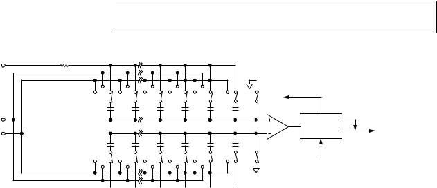
Figure 21. ADC Simplified Schematic
04657-021
CIRCUIT INFORMATION
The AD7942 is a fast, low power, single-supply, precise 14-bit ADC using successive approximation architecture.
The AD7942 is capable of converting 250,000 samples per second (250 kSPS) and powers down between conversions. When operating at 100 SPS, for example, it consumes typically 1.25 μW with a 2.5 V power supply, which is ideal for batterypowered applications.
The AD7942 provides the user with an on-chip track-and-hold and does not exhibit any pipeline delay or latency, making it ideal for multiple, multiplexed channel applications.
The AD7942 is specified from 2.3 V to 5.5 V and can be interfaced to a 1.8 V, 2.5 V, 3.3 V, or 5 V digital logic. It is housed in a 10-lead MSOP or a tiny 10-lead LFCSP that is space saving, yet allows flexible configurations. It is pin-for-pin-compatible with the 16-bit ADC AD7685.
CONVERTER OPERATION
The AD7942 is a successive approximation ADC based on a charge redistribution DAC. Figure 21 shows the simplified schematic of the ADC. The capacitive DAC consists of two identical arrays of 14 binary weighted capacitors, which are connected to the two comparator inputs.
During the acquisition phase, terminals of the array tied to the input of the comparator are connected to GND via SW+ and SW−. All independent switches are connected to the analog inputs. Thus, the capacitor arrays are used as sampling capacitors and acquire the analog signal on the IN+ and IN− inputs. When the acquisition phase is complete and the CNV input goes high, a conversion phase is initiated. When the conversion phase starts, SW+ and SW− are opened first. The two capacitor arrays are then disconnected from the inputs and connected to the GND input. Therefore, the differential voltage between the inputs (IN+ and IN−) captured at the end of the acquisition phase, is applied to the comparator inputs, causing the comparator to become unbalanced. By switching each element of the capacitor array between GND and REF, the comparator input varies by binary weighted voltage steps (VREF/2, VREF/4 ... VREF/16,384). The control logic toggles these switches, starting with the MSB, to bring the comparator back into a balanced condition. After the completion of this process, the part returns to the acquisition phase and the control logic generates the ADC output code and a busy signal indicator.
Because the AD7942 has an on-board conversion clock, the serial clock is not required for the conversion process.
Rev. C | Page 13 of 24