

AD7942 |
|
|
|
Data Sheet |
|
|
|
||
PIN CONFIGURATION AND FUNCTION DESCRIPTIONS |
||||
REF |
|
|
|
VIO |
|
|
|
||
1 |
|
10 |
||
VDD |
|
|
|
SDI |
2 |
|
9 |
||
IN+ |
|
AD7942 |
|
SCK |
3 |
8 |
|||
IN– |
|
|
|
SDO |
4 |
|
7 |
||
GND |
|
|
|
CNV |
5 |
|
6 |
||
|
|
|
|
|
NOTES
1.PADDLE CONNECTED TO GND. THIS CONNECTION IS NOT REQUIRED TO MEET THE ELECTRICAL PERFORMANCES.
Figure 4. Pin Configuration
04657-004
Table 6. Pin Function Descriptions
Pin No. |
Mnemonic |
Type1 |
Description |
1 |
REF |
AI |
Reference Input Voltage. The VREF range is from 0.5 V to VDD. REF is referred to the GND pin. Decouple REF |
|
|
|
as closely as possible to a 10 μF capacitor. |
2 |
VDD |
P |
Power Supply. |
3 |
IN+ |
AI |
Analog Input. IN+ is referred to IN−. The voltage range, that is, the difference between IN+ and IN−, is 0 V |
|
|
|
to VREF. |
4 |
IN− |
AI |
Analog Input Ground Sense. Connect IN− to the analog ground plane or to a remote sense ground. |
5 |
GND |
P |
Power Supply Ground. |
6 |
CNV |
DI |
Convert Input. This input pin has multiple functions. On its leading edge, CNV initiates the conversions |
|
|
|
and selects the interface mode of the part: chain mode or CS mode. In CS mode, CNV enables the SDO pin |
|
|
|
when low. In chain mode, the data should be read when CNV is high. |
7 |
SDO |
DO |
Serial Data Output. The conversion result is output on this pin. It is synchronized to SCK. |
8 |
SCK |
DI |
Serial Data Clock Input. When the part is selected, the conversion result is shifted out by this clock. |
9 |
SDI |
DI |
Serial Data Input. This input provides multiple features. It selects the interface mode of the ADC as follows: |
|
|
|
Chain mode is selected if SDI is low during the CNV rising edge. In this mode, SDI is used as a data input to |
|
|
|
daisy-chain the conversion results of two or more ADCs onto a single SDO line. The digital data level on |
|
|
|
SDI is output on SDO with a delay of 14 SCK cycles. |
|
|
|
CS mode is selected if SDI is high during the CNV rising edge. In this mode, either SDI or CNV can enable |
|
|
|
the serial output signals when low, and if SDI or CNV is low when the conversion is complete, the busy |
|
|
|
indicator feature is enabled. |
10 |
VIO |
P |
Input/Output Interface Digital Power. Nominally at the same supply as the host interface (1.8 V, 2.5 V, 3 V, or 5 V). |
|
|
|
|
1 AI = analog input, DI = digital input, DO = digital output, and P = power.
Rev. C | Page 8 of 24
Data Sheet
TYPICAL PERFORMANCE CHARACTERISTICS
|
1.00 |
|
|
|
|
|
|
|
|
|
|
|
|
|
|
|
|
|
|
|
|
|
|
|
|
|
|
|
|
|
|
|
|
|
|
|
|
|
|
|
|
POSITIVE INL = +0.22LSB |
|
|
|
|
|||||||||||
|
0.75 |
|
|
|
|
|
|
|
|
|
|
|
NEGATIVE INL = –0.34LSB |
|
|
|
|
|||||||||||
|
|
|
|
|
|
|
|
|
|
|
|
|
|
|
|
|
|
|
|
|
|
|
|
|
|
|
|
|
|
0.50 |
|
|
|
|
|
|
|
|
|
|
|
|
|
|
|
|
|
|
|
|
|
|
|
|
|
|
|
|
|
|
|
|
|
|
|
|
|
|
|
|
|
|
|
|
|
|
|
|
|
|
|
|
|
|
||
(LSB) |
0.25 |
|
|
|
|
|
|
|
|
|
|
|
|
|
|
|
|
|
|
|
|
|
|
|
|
|
|
|
|
|
|
|
|
|
|
|
|
|
|
|
|
|
|
|
|
|
|
|
|
|
|
|
|
|
|||
0 |
|
|
|
|
|
|
|
|
|
|
|
|
|
|
|
|
|
|
|
|
|
|
|
|
|
|
|
|
|
|
|
|
|
|
|
|
|
|
|
|
|
|
|
|
|
|
|
|
|
|
|
|
|
|
|
||
INL |
|
|
|
|
|
|
|
|
|
|
|
|
|
|
|
|
|
|
|
|
|
|
|
|
|
|
|
|
–0.25 |
|
|
|
|
|
|
|
|
|
|
|
|
|
|
|
|
|
|
|
|
|
|
|
|
|
|
||
|
|
|
|
|
|
|
|
|
|
|
|
|
|
|
|
|
|
|
|
|
|
|
|
|
|
|
||
|
|
|
|
|
|
|
|
|
|
|
|
|
|
|
|
|
|
|
|
|
|
|
|
|
|
|
||
|
–0.50 |
|
|
|
|
|
|
|
|
|
|
|
|
|
|
|
|
|
|
|
|
|
|
|
|
|
|
|
|
|
|
|
|
|
|
|
|
|
|
|
|
|
|
|
|
|
|
|
|
|
|
|
|
|
|
||
|
–0.75 |
|
|
|
|
|
|
|
|
|
|
|
|
|
|
|
|
|
|
|
|
|
|
|
|
04657-005 |
||
|
|
|
|
|
|
|
|
|
|
|
|
|
|
|
|
|
|
|
|
|
|
|
|
|
||||
|
–1.00 |
|
|
|
|
|
|
|
|
|
|
|
|
|
|
|
|
|
|
|
|
|
|
|
|
|||
|
|
|
|
|
|
|
|
|
|
|
|
|
|
|
|
|
|
|
|
|
|
|
|
|
|
|
||
|
0 |
4096 |
|
|
8192 |
|
|
|
|
|
|
12,288 |
|
16,384 |
||||||||||||||
|
|
|
|
|
|
|
|
|
|
CODE |
|
|
|
|
|
|
|
|
|
|
|
|
|
|
|
|||
|
|
|
|
Figure 5. Integral Nonlinearity vs. Code |
|
|
|
|
|
|||||||||||||||||||
150,000 |
|
|
|
|
|
|
|
|
|
|
|
|
|
|
|
|
|
|
|
|
|
|
|
|
|
|
|
|
|
|
|
|
|
|
|
|
|
|
|
|
|
|
|
|
|
|
|
|
|
|
|
|
|
|
|||
|
|
|
|
|
|
|
|
|
|
129,941 |
|
|
|
|
VDD = VREF = 2.5V |
|
|
|
|
|||||||||
100,000 |
|
|
|
|
|
|
|
|
|
|
|
|
|
|
|
|
|
|
|
|
|
|
|
|
|
|
|
|
|
|
|
|
|
|
|
|
|
|
|
|
|
|
|
|
|
|
|
|
|
|
|
|
|
|
|||
COUNTS |
|
|
|
|
|
|
|
|
|
|
|
|
|
|
|
|
|
|
|
|
|
|
|
|
|
|
|
|
|
50,000 |
|
|
|
|
|
|
|
|
|
|
|
|
|
|
|
|
|
|
|
|
|
|
|
|
|
|
-006 |
|
|
|
|
|
|
|
|
|
|
|
|
|
|
|
|
|
|
|
|
|
|
|
|
|
|
|||
|
|
|
|
|
|
|
|
|
|
|
|
|
|
|
|
|
|
|
|
|
|
|
|
|
|
|
|
|
|
|
|
|
0 |
0 |
|
915 |
|
|
|
|
|
|
216 |
|
0 |
|
0 |
|
|
|
04657 |
||||||
|
0 |
|
|
|
|
|
|
|
|
|
|
|
|
|
|
|
|
|
|
|
|
|
|
|
|
|
|
|
|
|
1FFD |
1FFE |
1FFF |
2000 |
2001 |
2002 |
|
2003 |
|
|
|
|
|||||||||||||||
|
|
|
|
|
|
|
|
|
||||||||||||||||||||
|
|
|
|
|
|
|
|
|
CODE IN HEX |
|
|
|
|
|
|
|
|
|
|
|||||||||
|
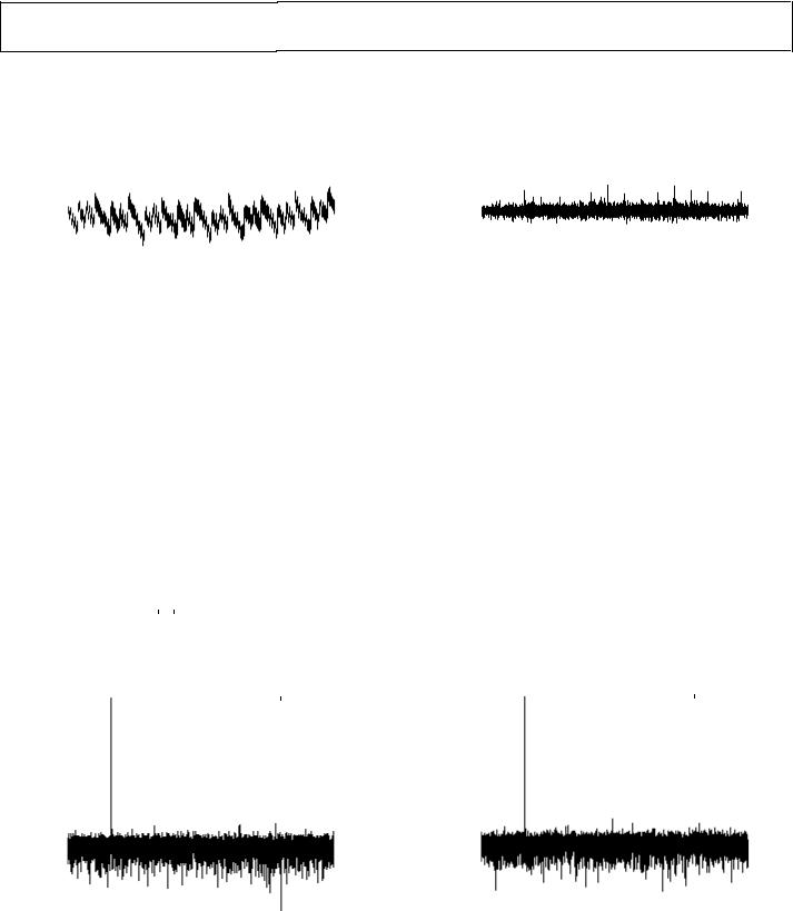
Figure 6. Histogram of a DC Input at the Code Center |
|
|
|
|
|||||||||||||||||||||||
|
0 |
|
|
|
|
|
|
|
|
|
|
|
|
|
|
|
|
|
|
|
|
|
|
|
|
|
|
|
|
|
|
|
|
|
|
|
|
|
|
|
|
|
|
|
|
16,384 POINT FFT |
|
|
|
|
|||||||
|
|
|
|
|
|
|
|
|
|
|
|
|
|
|
|
|
|
|
|
|
|
|||||||
|
–20 |
|
|
|
|
|
|
|
|
|
|
|
|
|
|
|
VDD = VREF = 5V |
|
|
|
|
|||||||
|
|
|
|
|
|
|
|
|
|
|
|
|
|
|
|
|
|
|
|
|
||||||||
|
|
|
|
|
|
|
|
|
|
|
|
|
|
|
|
|
|
fS = 250kSPS |
|
|
|
|
|
|||||
Scale) |
–40 |
|
|
|
|
|
|
|
|
|
|
|
|
|
|
|
fIN = 20.43kHz |
|
|
|
|
|||||||
|
|
|
|
|
|
|
|
|
|
|
|
|
|
|
|
|
|
|
|
|||||||||
|
|
|
|
|
|
|
|
|
|
|
|
|
|
|
|
|
SNR = 85.1dB |
|
|
|
|
|||||||
|
|
|
|
|
|
|
|
|
|
|
|
|
|
|
|
|
|
|
|
|
|
|||||||
Full |
–60 |
|
|
|
|
|
|
|
|
|
|
|
|
|
|
|
THD = –105dB |
|
|
|
|
|||||||
|
|
|
|
|
|
|
|
|
|
|
|
|
|
|
|
|
|
|
|
|||||||||
|
|
|
|
|
|
|
|
|
|
|
|
|
|
|
|
|
SFDR = –105.9dB |
|
|
|
|
|||||||
of |
–80 |
|
|
|
|
|
|
|
|
|
|
|
|
|
|
|
|
|
|
|
|
|
|
|
|
|
|
|
|
|
|
|
|
|
|
|
|
|
|
|
|
|
|
|
|
|
|
|
|
|
|
|
|
|
|
||
(dB |
–100 |
|
|
|
|
|
|
|
|
|
|
|
|
|
|
|
|
|
|
|
|
|
|
|
|
|
|
|
AMPLITUDE |
|
|
|
|
|
|
|
|
|
|
|
|
|
|
|
|
|
|
|
|
|
|
|
|
|
|
||
|
|
|
|
|
|
|
|
|
|
|
|
|
|
|
|
|
|
|
|
|
|
|
|
|
|
|
||
–140 |
|
|
|
|
|
|
|
|
|
|
|
|
|
|
|
|
|
|
|
|
|
|
|
|
|
|
||
|
–120 |
|
|
|
|
|
|
|
|
|
|
|
|
|
|
|
|
|
|
|
|
|
|
|
|
|
-007 |
|
|
–160 |
|
|
|
|
|
|
|
|
|
|
|
|
|
|
|
|
|
|
|
|
|
|
|
|
|
||
|
|
|
|
|
|
|
|
|
|
|
|
|
|
|
|
|
|
|
|
|
|
|
|
|
|
|||
|
–180 |
|
|
|
|
|
|
|
|
|
|
|
|
|
|
|
|
|
|
|
|
|
|
|
|
04657 |
||
|
|
|
25 |
|
50 |
|
|
|
|
75 |
|
|
100 |
|
|
125 |
||||||||||||
|
0 |
|
|
|
|
|
|
|
|
|
|
|||||||||||||||||
FREQUENCY (kHz)
Figure 7. FFT Plot
AD7942
|
1.00 |
|
|
|
|
|
|
|
|
|
|
|
|
|
|
|
|
|
|
|
|
|
|
|
|
|
|
|
|
|
|
|
|
|
|
|
POSITIVE DNL = +0.24LSB |
|
|
|
|||||||||
|
0.75 |
|
|
|
|
|
|
|
|
|
|
NEGATIVE DNL = –0.12LSB |
|
|
|
|||||||||
|
|
|
|
|
|
|
|
|
|
|
|
|
|
|
|
|
|
|
|
|
|
|
|
|
|
0.50 |
|
|
|
|
|
|
|
|
|
|
|
|
|
|
|
|
|
|
|
|
|
|
|
|
|
|
|
|
|
|
|
|
|
|
|
|
|
|
|
|
|
|
|
|
|
|
||
(LSB) |
0.25 |
|
|
|
|
|
|
|
|
|
|
|
|
|
|
|
|
|
|
|
|
|
|
|
|
|
|
|
|
|
|
|
|
|
|
|
|
|
|
|
|
|
|
|
|
|
|||
0 |
|
|
|
|
|
|
|
|
|
|
|
|
|
|
|
|
|
|
|
|
|
|
|
|
DNL |
|
|
|
|
|
|
|
|
|
|
|
|
|
|
|
|
|
|
|
|
|
|
|
|
–0.25 |
|
|
|
|
|
|
|
|
|
|
|
|
|
|
|
|
|
|
|
|
|
|
||
|
|
|
|
|
|
|
|
|
|
|
|
|
|
|
|
|
|
|
|
|
|
|
||
|
|
|
|
|
|
|
|
|
|
|
|
|
|
|
|
|
|
|
|
|
|
|
||
|
–0.50 |
|
|
|
|
|
|
|
|
|
|
|
|
|
|
|
|
|
|
|
|
|
|
|
|
|
|
|
|
|
|
|
|
|
|
|
|
|
|
|
|
|
|
|
|
|
|
||
|
–0.75 |
|
|
|
|
|
|
|
|
|
|
|
|
|
|
|
|
|
|
|
|
04657-008 |
||
|
|
|
|
|
|
|
|
|
|
|
|
|
|
|
|
|
|
|
|
|
||||
|
|
|
|
|
|
|
|
|
|
|
|
|
|
|
|
|
|
|
|
|
|
|
||
|
–1.00 |
|
|
|
|
|
|
|
|
|
|
|
|
|
|
|
|
|
|
|
|
|
||
|
0 |
4096 |
8192 |
|
|
|
|
12,288 |
|
16,384 |
||||||||||||||
|
|
|
|
|
|
|
|
|
CODE |
|
|
|
|
|
|
|
|
|
|
|
|
|||
|
|
|
Figure 8. Differential Nonlinearity vs. Code |
|
|
|
|
|||||||||||||||||
150,000 |
|
|
|
|
|
|
|
|
|
|
|
|
|
|
|
|
|
|
|
|
|
|
|
|
|
|
|
|
|
|
|
|
|
|
|
|
|
|
|
|
|
|
|
|
|
|
|||
|
|
|
|
|
|
|
|
|
131,072 |
|
|
|
VDD = VREF = 5V |
|
|
|
||||||||
100,000 |
|
|
|
|
|
|
|
|
|
|
|
|
|
|
|
|
|
|
|
|
|
|
|
|
|
|
|
|
|
|
|
|
|
|
|
|
|
|
|
|
|
|
|
|
|
|
|||
COUNTS |
|
|
|
|
|
|
|
|
|
|
|
|
|
|
|
|
|
|
|
|
|
|
|
|
|
50,000 |
|
|
|
|
|
|
|
|
|
|
|
|
|
|
|
|
|
|
|
|
|
|
04657-009 |
|
0 |
0 |
|
0 |
|
|
|
|
|
0 |
|
|
0 |
|
0 |
|
|
|||||||
|
0 |
|
|
|
|
|
|
|
|
|
|
|
|
|||||||||||
|
|
1FFD |
1FFE |
1FFF 2000 |
2001 |
2002 |
|
2003 |
|
|
|
|||||||||||||
|
|
|
|
|
|
|
||||||||||||||||||
|
|
|
|
|
|
|
|
CODE IN HEX |
|
|
|
|
|
|
|
|
|
|||||||
|
Figure 9. Histogram of a DC Input at the Code Center |
|
|
|
||||||||||||||||||||
|
0 |
|
|
|
|
|
|
|
|
|
|
|
|
|
|
|
|
|
|
|
|
|
|
|
|
|
|
|
|
|
|
|
|
|
|
|
|
|
16,384 POINT FFT |
|
|
|
|||||||
|
|
|
|
|
|
|
|
|
|
|
|
|
|
|
|
|
|
|||||||
|
–20 |
|
|
|
|
|
|
|
|
|
|
|
|
|
VDD = VREF = 2.5V |
|
|
|
||||||
|
|
|
|
|
|
|
|
|
|
|
|
|
|
|
|
|
||||||||
|
|
|
|
|
|
|
|
|
|
|
|
|
|
|
fS = 250kSPS |
|
|
|
|
|||||
Scale) |
–40 |
|
|
|
|
|
|
|
|
|
|
|
|
|
fIN = 20.43kHz |
|
|
|
||||||
|
|
|
|
|
|
|
|
|
|
|
|
|
|
|
|
|||||||||
|
|
|
|
|
|
|
|
|
|
|
|
|
|
SNR = 84.2dB |
|
|
|
|||||||
|
|
|
|
|
|
|
|
|
|
|
|
|
|
|
|
|
|
|||||||
Full |
–60 |
|
|
|
|
|
|
|
|
|
|
|
|
|
THD = –101.7dB |
|
|
|
||||||
|
|
|
|
|
|
|
|
|
|
|
|
|
|
|
|
|||||||||
|
|
|
|
|
|
|
|
|
|
|
|
|
|
SFDR = –104.3dB |
|
|
|
|||||||
of |
–80 |
|
|
|
|
|
|
|
|
|
|
|
|
|
|
|
|
|
|
|
|
|
|
|
|
|
|
|
|
|
|
|
|
|
|
|
|
|
|
|
|
|
|
|
|
|
|
||
(dB |
–100 |
|
|
|
|
|
|
|
|
|
|
|
|
|
|
|
|
|
|
|
|
|
|
|
AMPLITUDE |
|
|
|
|
|
|
|
|
|
|
|
|
|
|
|
|
|
|
|
|
|
|
|
|
|
|
|
|
|
|
|
|
|
|
|
|
|
|
|
|
|
|
|
|
|
|
|
||
–140 |
|
|
|
|
|
|
|
|
|
|
|
|
|
|
|
|
|
|
|
|
|
|
|
|
|
–120 |
|
|
|
|
|
|
|
|
|
|
|
|
|
|
|
|
|
|
|
|
|
-010 |
|
|
–160 |
|
|
|
|
|
|
|
|
|
|
|
|
|
|
|
|
|
|
|
|
|
||
|
|
|
|
|
|
|
|
|
|
|
|
|
|
|
|
|
|
|
|
|
|
|||
|
–180 |
|
|
|
|
|
|
|
|
|
|
|
|
|
|
|
|
|
|
|
|
|
04657 |
|
|
|
|
25 |
|
50 |
|
|
|
|
75 |
|
100 |
|
|
125 |
|||||||||
|
0 |
|
|
|
|
|
|
|
|
|
||||||||||||||
FREQUENCY (kHz)
Figure 10. FFT Plot
Rev. C | Page 9 of 24
AD7942 |
|
|
|
|
|
|
|
|
|
|
|
|
|
|
Data Sheet |
|
86 |
|
|
|
|
|
|
15.0 |
|
|
–80 |
|
|
|
|
|
|
|
|
|
|
SNR |
|
|
|
|
|
|
|
|
|
|
|
|
|
|
|
|
|
|
|
|
|
|
–85 |
|
|
|
|
|
|
85 |
|
|
|
|
|
|
14.5 |
|
|
–90 |
|
|
VREF = 2.5V, –1dB |
|
|
|
SINADSNR,(dB) |
|
|
|
|
|
|
|
(Bits)ENOB |
(dB)THD |
|
|
|
|
|
|
|
|
SINAD |
|
|
|
|
–95 |
|
|
|
|
|
|
||||
|
|
|
|
|
|
|
|
|
|
|
|
|
|
|||
84 |
|
|
|
|
|
|
14.0 |
|
|
|
|
|
|
VREF = 5V, –1dB |
|
|
|
|
|
|
|
|
|
|
|
|
–100 |
|
|
|
|
|
|
83 |
|
|
|
ENOB |
|
|
13.5 |
|
|
–105 |
|
|
|
|
|
|
|
|
|
|
|
|
|
|
|
|
|
|
|
|
|
||
|
|
|
|
|
|
|
|
04657-011 |
|
–110 |
|
|
|
|
|
04657-014 |
822.0 |
|
|
|
|
|
|
5.513.0 |
|
–115 |
|
|
|
|
|
||
2.5 |
3.0 |
3.5 |
4.0 |
4.5 |
5.0 |
|
|
0 |
40 |
80 |
120 |
160 |
200 |
|||
|
|
REFERENCE VOLTAGE (V) |
|
|
|
|
|
|
|
FREQUENCY (kHz) |
|
|
||||
|
|
|
|
|
|
|
|
|
|
|
|
|
|
|
||
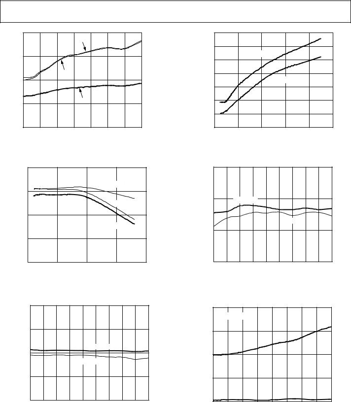
Figure 11. SNR, SINAD, and ENOB vs. Reference Voltage
|
90 |
|
|
|
|
|
|
|
VREF = 5V, –10dB |
|
|
|
85 |
|
|
|
|
(dB) |
|
|
|
VREF = 5V, –1dB |
|
80 |
|
|
|
|
|
SINAD |
|
|
|
|
|
|
|
VREF |
= 2.5V, –1dB |
|
|
|
|
|
|
||
|
75 |
|
|
|
|
|
70 0 |
|
|
|
04657-012 |
|
50 |
100 |
150 |
200 |
|
|
|
|
FREQUENCY (kHz) |
|
|
Figure 14. THD vs. Frequency
–90
–100 |
|
VREF = 2.5V |
|
|
|
|
|
|
||
THD (dB) |
|
|
|
|
|
VREF = 5V |
|
|
|
|
–110 |
|
|
|
|
|
|
|
|
|
|
–120 |
|
|
|
|
|
|
|
|
04657-015 |
|
–35 |
–15 |
5 |
25 |
45 |
65 |
85 |
105 |
125 |
||
–55 |
||||||||||
TEMPERATURE (°C)
Figure 12. SINAD vs. Frequency
|
95 |
|
|
|
|
|
|
|
|
|
|
90 |
|
|
|
|
|
|
|
|
|
(dB) |
|
|
|
|
|
VREF = 5V |
|
|
|
|
85 |
|
|
|
|
|
|
|
|
|
|
SNR |
|
|
|
|
|
|
|
|
|
|
|
|
|
|
VREF = 2.5V |
|
|
|
|
||
|
|
|
|
|
|
|
|
|
||
|
80 |
|
|
|
|
|
|
|
|
|
|
75 |
|
|
|
|
|
|
|
|
04657-013 |
|
–35 |
–15 |
5 |
25 |
45 |
65 |
85 |
105 |
125 |
|
|
–55 |
|||||||||
TEMPERATURE (°C)
Figure 15. THD vs. Temperature
|
1000 |
|
|
|
|
|
|
|
|
|
|
fS = 100kSPS |
|
|
|
|
|
|
|
A) |
750 |
|
|
|
|
|
|
|
|
(μ |
|
|
|
|
|
|
|
|
|
|
|
|
|
|
|
|
|
|
|
CURRENTS |
|
|
|
|
VDD |
|
|
|
|
500 |
|
|
|
|
|
|
|
|
|
OPERATING |
250 |
|
|
|
|
|
|
|
|
|
|
|
|
|
|
|
|
|
|
|
|
|
|
|
VIO |
|
|
|
-016 |
|
0 |
|
|
|
|
|
|
04657 |
|
|
|
|
|
|
|
|
|
||
|
2.7 |
3.1 |
3.5 |
3.9 |
4.3 |
4.7 |
5.1 |
5.5 |
|
|
2.3 |
||||||||
|
|
|
|
|
SUPPLY (V) |
|
|
|
|
Figure 13. SNR vs. Temperature |
Figure 16. Operating Currents vs. Supply |
Rev. C | Page 10 of 24
Data Sheet
|
1000 |
|
|
|
|
|
|
|
|
|
(nA) |
750 |
|
|
|
|
|
|
|
|
|
CURRENTS |
500 |
|
|
|
|
|
|
|
|
|
DOWN |
|
|
|
|
|
|
|
|
|
|
|
|
|
|
|
|
|
|
|
|
|
POWER- |
|
|
|
|
|
|
VDD + VIO |
|
|
|
250 |
|
|
|
|
|
|
|
|
|
|
|
|
|
|
|
|
|
|
|
|
|
|
0 |
|
|
|
|
|
|
|
|
04657-017 |
|
–35 |
–15 |
5 |
25 |
45 |
65 |
85 |
105 |
125 |
|
|
–55 |
|||||||||
TEMPERATURE (°C)
Figure 17. Power-Down Currents vs. Temperature
|
1000 |
|
|
|
|
|
|
fS = 100kSPS |
|
|
|
900 |
|
|
|
|
|
|
|
||
|
|
|
|
|
|
|
|
|
|
|
(µA) |
800 |
|
|
|
VDD = 5V |
|
|
|
|
|
700 |
|
|
|
|
|
|
|
|
|
|
CURRENTS |
|
|
|
|
|
|
|
|
|
|
600 |
|
|
|
VDD = 2.5V |
|
|
|
|
||
500 |
|
|
|
|
|
|
|
|||
|
|
|
|
|
|
|
|
|
||
OPERATING |
400 |
|
|
|
|
|
|
|
|
|
300 |
|
|
|
|
|
|
|
|
|
|
200 |
|
|
|
|
|
|
|
|
|
|
|
|
|
|
|
|
|
|
|
|
|
|
100 |
|
|
|
|
VIO |
|
|
|
04657-018 |
|
|
|
|
|
|
|
|
|
||
|
0 |
|
|
|
|
|
|
|
|
|
|
–35 |
–15 |
5 |
25 |
45 |
65 |
85 |
105 |
125 |
|
|
–55 |
|||||||||
|
|
|
|
TEMPERATURE (°C) |
|
|
|
|||
Figure 18. Operating Currents vs. Temperature
|
|
|
|
|
|
|
|
|
AD7942 |
|
|
6 |
|
|
|
|
|
|
|
|
|
|
5 |
|
|
|
|
|
|
|
|
|
(LSB) |
4 |
|
|
|
|
|
|
|
|
|
3 |
|
|
|
|
|
|
|
|
|
|
ERROR |
2 |
|
|
|
|
|
|
|
|
|
1 |
|
|
|
|
OFFSET ERROR |
|
|
|||
GAIN |
0 |
|
|
|
|
|
|
|||
|
|
|
|
|
|
|
|
|
||
–1 |
|
|
|
|
|
|
|
|
|
|
AND |
|
|
|
|
|
|
|
|
|
|
–2 |
|
|
|
|
GAIN ERROR |
|
|
|
||
OFFSET |
|
|
|
|
|
|
|
|||
–3 |
|
|
|
|
|
|
|
|
|
|
–4 |
|
|
|
|
|
|
|
|
|
|
|
|
|
|
|
|
|
|
|
04657-019 |
|
|
–5 |
|
|
|
|
|
|
|
|
|
|
–6 |
|
|
|
|
|
|
|
|
|
|
–35 |
–15 |
5 |
25 |
45 |
65 |
85 |
105 |
125 |
|
|
–55 |
|||||||||
|
|
|
|
TEMPERATURE (°C) |
|
|
|
|||
Figure 19. Offset Error and Gain Error vs. Temperature
|
25 |
|
|
|
|
|
|
|
20 |
|
VDD = 2.5V, 85°C |
|
|
||
(ns) |
15 |
|
|
|
|
|
|
DELAY |
|
|
VDD = 2.5V, 25°C |
|
|
|
|
10 |
|
|
|
|
|
|
|
DSDO |
|
|
|
|
|
|
|
|
|
|
|
|
VDD = 5V, 85°C |
|
|
t |
|
|
|
|
|
|
|
|
5 |
|
VDD = 3.3V, 85°C |
VDD = 5V, 25°C |
|
||
|
|
|
|
|
-020 |
||
|
|
VDD = 3.3V, 25°C |
|
|
|
||
|
|
|
|
|
04657 |
||
|
0 |
|
|
|
|
|
|
|
20 |
40 |
60 |
80 |
100 |
120 |
|
|
0 |
||||||
|
|
|
SDO CAPACITIVE LOAD (pF) |
|
|||
Figure 20. tDSDO Delay vs. SDO Capacitance Load and Supply
Rev. C | Page 11 of 24