

AD7942
Power Supply
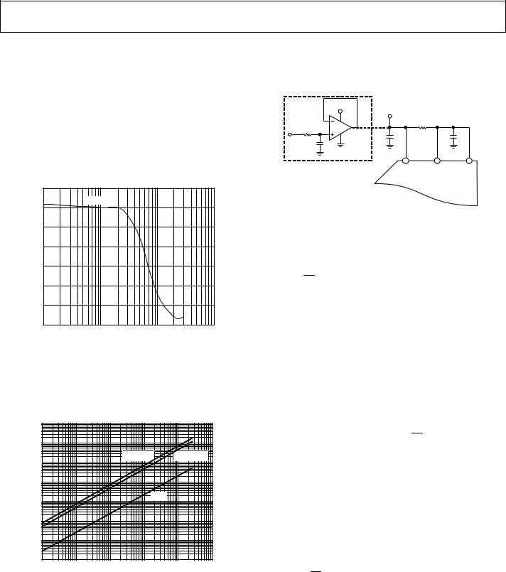
The AD7942 is specified over a wide operating range from 2.3 V to 5.5 V. It has, unlike other low voltage converters, a noise low enough to design a low supply (2.5 V) 14-bit resolution system with respectable performance. It uses two power supply pins: a core supply, VDD, and a digital input/output interface supply, VIO. VIO allows direct interface with any logic between 1.8 V and VDD. To reduce the supplies needed, the VIO and VDD can be tied together. The AD7942 is independent of power supply sequencing between VIO and VDD. Additionally, it is insensitive to power supply variations over a wide frequency range, as shown in Figure 27.
|
90 |
|
|
|
|
85 |
VDD = 5V |
|
|
|
|
|
|
|
PSRR(dB) |
80 |
|
|
|
70 |
|
|
|
|
|
75 |
|
|
|
|
65 |
|
|
|
|
60 |
|
|
04657-027 |
|
55 |
|
|
|
|
100 |
1000 |
10000 |
|
|
10 |
FREQUENCY (kHz)
Figure 27. PSRR vs. Frequency
The AD7942 powers down automatically at the end of each conversion phase and, therefore, the power scales linearly with the sampling rate, as shown in Figure 28. This makes the part ideal for low sampling rates (even rates of a few hertz) and low battery-powered applications.
|
1000 |
|
|
|
|
|
(µA) |
|
|
|
VDD = 5V |
VDD = 2.5V |
|
|
|
|
|
|
|
|
CURRENT |
10 |
|
|
|
|
|
|
|
|
|
VIO |
|
|
OPERATING |
0.1 |
|
|
|
|
|
|
|
|
|
|
|
|
0.00110 |
|
|
|
|
04657-028 |
|
100 |
1000 |
10000 |
100000 |
1000000 |
||
|
|
|
SAMPLING RATE (SPS) |
|
||
Figure 28. Operating Current vs. Sampling Rate
Supplying the ADC from the Reference
For simplified applications, the AD7942, with its low operating current, can be supplied directly using the reference circuit, as shown in Figure 29. The reference line can be driven by either
The system power supply directly,
Data Sheet
A reference voltage with enough current output capability, such as the ADR43x, or
A reference buffer, such as the AD8031, that can also filter the system power supply (see Figure 29).
5V
10Ω
10µF |
|
1µF |
1µF |
|
|
(NOTE 1) |
|
|
REF |
VDD |
VIO |
AD7942 |
|
NOTE 1: OPTIONAL REFERENCE BUFFER AND FILTER. |
04657-029 |
Figure 29. Example of Application Circuit
DIGITAL INTERFACE
Although the AD7942 has a reduced number of pins, it offers flexibility in its serial interface modes.
When in CS mode, the AD7942 is compatible with SPI, QSPI, digital hosts, and DSPs (for example, Blackfin® ADSP-BF53x or ADSP-219x). A 3-wire interface using the CNV, SCK, and SDO signals minimizes wiring connections, which is useful, for instance, in isolated applications. A 4-wire interface using the SDI, CNV, SCK, and SDO signals allows CNV, which initiates conversions, to be independent of the readback timing (SDI). This is useful in low jitter sampling or simultaneous sampling applications.
When in chain mode, the AD7942 provides a daisy-chain feature using the SDI input for cascading multiple ADCs on a single data line similar to a shift register.
The mode in which the part operates depends on the SDI level when the CNV rising edge occurs. The CS mode is selected if SDI is high and the chain mode is selected if SDI is low. The SDI hold time is such that when SDI and CNV are connected together, the chain mode is always selected.
In either mode, the AD7942 offers the flexibility to optionally force a start bit in front of the data bits. This start bit can be used as a busy signal indicator to interrupt the digital host and trigger the data reading. Otherwise, without a busy indicator, the user must time out the maximum conversion time prior to readback.
The busy indicator feature is enabled as follows:
In the CS mode, if CNV or SDI is low when the ADC conversion ends (see Figure 33 and Figure 37).
In the chain mode, if SCK is high during the CNV rising edge (see Figure 41).
Rev. C | Page 16 of 24
Data Sheet |
AD7942 |
|
|
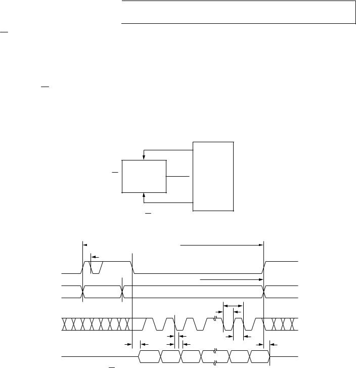
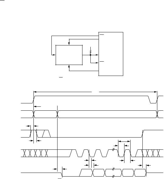
CS Mode 3-Wire Without Busy Indicator
This mode is most often used when a single AD7942 is connected to an SPI-compatible digital host. The connection diagram is shown in Figure 30 and the corresponding timing diagram is shown in Figure 31.
With SDI tied to VIO, a rising edge on CNV initiates a conversion, selects the CS mode, and forces SDO to high impedance. When a conversion is initiated, it continues to completion irrespective of the state of CNV. For instance, it is useful to bring CNV low to select other SPI devices, such as analog multiplexers. However, CNV must be returned high before the
CNV
VIO
 SDI AD7942 SDO
SCK
minimum conversion time and held high until the maximum conversion time to avoid generating the busy signal indicator. When the conversion is complete the AD7942 enters the acquisition phase and powers down. When CNV goes low, the MSB is output onto SDO. The remaining data bits are then clocked by subsequent SCK falling edges. The data is valid on both SCK edges. Although the rising edge can be used to capture the data, a digital host also using the SCK falling edge allows a faster reading rate provided it has an acceptable hold time. After the 14th SCK falling edge or when CNV goes high, whichever is earlier, SDO returns to high impedance.
CONVERT
DIGITAL HOST
 DATA IN
CLK |
04657-030 |
|
Figure 30. CS Mode 3-Wire Without Busy Indicator
Connection Diagram (SDI High)
SDI = 1 |
|
tCYC |
|
tCNVH 
CNV
 tCONV
tCONV 
 tACQ
tACQ
ACQUISITION |
CONVERSION |
|
ACQUISITION |
|
|
|
|
|
|
|
|
tSCK |
|
|
|
|
|
tSCKL |
|
|
SCK |
1 |
2 |
3 |
12 |
13 |
14 |
|
|
tHSDO |
|
tSCKH |
|
|
|
tEN |
|
tDSDO |
|
|
tDIS |
SDO |
D13 |
D12 |
D11 |
|
D1 |
D0 |
Figure 31. CS Mode 3-Wire Without Busy Indicator, Serial Interface Timing (SDI High)
04657-031
Rev. C | Page 17 of 24
|
AD7942 |
Data Sheet |
|
|
|
|
|
|
|
|
|
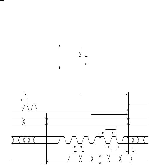
CS Mode 3-Wire with Busy Indicator
This mode is most often used when a single AD7942 is connected to an SPI-compatible digital host with an interrupt input. The connection diagram is shown in Figure 32 and the corresponding timing diagram is shown in Figure 33.
With SDI tied to VIO, a rising edge on CNV initiates a conversion, selects the CS mode, and forces SDO to high impedance. SDO is maintained in high impedance until the completion of the conversion irrespective of the state of CNV. Prior to the minimum conversion time, CNV can be used to select other SPI devices, such as analog multiplexers. However, CNV must be returned low before the minimum conversion time and held
low until the maximum conversion time to guarantee the generation of the busy signal indicator. When the conversion is complete, SDO goes from high impedance to low impedance. With a pull-up on the SDO line, this transition can be used as an interrupt signal to initiate the data reading controlled by the digital host. The AD7942 then enters the acquisition phase and powers down. The data bits are then clocked out, MSB first, by subsequent SCK falling edges. The data is valid on both SCK edges. Although the rising edge can be used to capture the data, a digital host also using the SCK falling edge allows a faster reading rate provided it has an acceptable hold time. After
the optional 15th SCK falling edge or when CNV goes high, whichever is earlier, SDO returns to high impedance.
|
|
|
|
|
|
|
|
|
|
CONVERT |
||
|
|
|
|
|
|
|
VIO |
|||||
|
|
|
|
|
|
|
|
DIGITAL HOST |
||||
|
|
|
|
|
|
|
|
|||||
|
|
|
CNV |
|
||||||||
|
|
|
|
|
|
|
||||||
VIO |
|
|
|
|
|
47kΩ |
|
|
|
|||
|
|
|
SDI AD7942 SDO |
|
|
|
DATA IN |
|||||
|
|
|
|
|
|
|||||||
|
|
|
SCK |
|
|
|
|
|
|
|||
|
|
|
|
|
|
IRQ |
||||||
|
|
|
|
|
|
|||||||
|
|
|
|
|
|
|
|
|
|
CLK |
||
|
|
|
|
|
|
|
|
|
|
|||
|
|
|
|
|
|
|
|
|
|
|||
|
|
|
|
|
|
|
|
|
|
|
|
|
04657-032
Figure 32. CS Mode 3-Wire with Busy Indicator
Connection Diagram (SDI High)
SDI = 1 |
|
tCYC |
|
 tCNVH
tCNVH
CNV
 tCONV
tCONV 
 tACQ
tACQ
ACQUISITION |
CONVERSION |
|
ACQUISITION |
|
|
|
|
|
|
|
|
tSCK |
|
|
|
|
|
tSCKL |
|
|
SCK |
1 |
2 |
3 |
13 |
14 |
15 |
|
tHSDO |
|
|
tSCKH |
|
|
|
tDSDO |
|
|
|
|
tDIS |
SDO |
|
D13 |
D12 |
|
D1 |
D0 |
04657-033
Figure 33. CS Mode 3-Wire with Busy Indicator, Serial Interface Timing (SDI High)
Rev. C | Page 18 of 24
Data Sheet |
AD7942 |
||
|
|
|
|
|
|
|
|
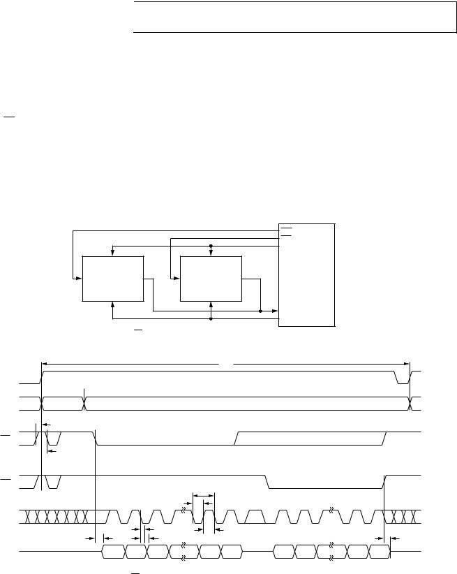
CS Mode 4-Wire Without Busy Indicator
This mode is most often used when multiple AD7942s are connected to an SPI-compatible digital host. A connection diagram using two AD7942s is shown in Figure 34 and the corresponding timing diagram is given in Figure 35.
With SDI high, a rising edge on CNV initiates a conversion, selects the CS mode, and forces SDO to high impedance. In this mode, CNV must be held high during the conversion phase and the subsequent data readback (if SDI and CNV are low, SDO is driven low). Prior to the minimum conversion time, SDI can be used to select other SPI devices, such as analog multiplexers. However, SDI must be returned high before the minimum conversion time elapses and held high until the maximum conversion time is completed to avoid generating the busy signal indicator. When the conversion is complete, the AD7942
enters the acquisition phase and powers down. Each ADC result can be read by bringing its SDI input low, which consequently outputs the MSB onto SDO. The remaining data bits are then clocked by subsequent SCK driving edges. The data is valid on both SCK edges. Although the nondriving edge can be used to capture the data, a digital host also using the SCK falling edge allows a faster reading rate, provided it has an acceptable hold time. After the 14th SCK falling edge or when SDI goes high, whichever is earlier, SDO returns to high impedance and another AD7942 can be read.
If multiple AD7942s are selected at the same time, the SDO output pin handles this contention without damage or induced latch-up. Meanwhile, it is recommended to keep this contention as short as possible to limit extra power dissipation.
|
|
|
|
CS2 |
|
|
|
|
|
CS1 |
|
|
|
|
|
CONVERT |
|
|
CNV |
|
CNV |
DIGITAL HOST |
|
SDI |
AD7942 SDO |
SDI |
AD7942 SDO |
|
|
|
SCK |
|
SCK |
|
|
|
|
|
|
DATA IN |
04657-034 |
|
|
|
|
CLK |
|
|
|
|
|
|
Figure 34. CS Mode 4-Wire Without Busy Indicator Connection Diagram
tCYC
CNV
 tCONV
tCONV 
 tACQ
tACQ 
ACQUISITION |
CONVERSION |
ACQUISITION |
tSSDICNV 
SDI (CS1)
tHSDICNV 
SDI (CS2)
|
|
|
|
|
tSCK |
|
|
|
|
|
|
|
|
|
|
tSCKL |
|
|
|
|
|
|
|
SCK |
1 |
2 |
3 |
12 |
13 |
14 |
15 |
16 |
26 |
27 |
28 |
|
tHSDO |
|
|
tSCKH |
|
|
|
|
|
|
|
|
tEN |
|
|
tDSDO |
|
|
|
|
|
|
tDIS |
SDO |
D13 |
D12 |
D11 |
D1 |
D0 |
D13 |
D12 |
|
D1 |
D0 |
|
04657-035
Figure 35. CS Mode 4-Wire Without Busy Indicator, Serial Interface Timing
Rev. C | Page 19 of 24
|
AD7942 |
Data Sheet |
|
|
|
|
|
|
|
|
|
CS Mode 4-Wire with Busy Indicator
This mode is most often used when a single AD7942 is connected to an SPI-compatible digital host with an interrupt input and to keep CNV (which is used to sample the analog input) independent of the signal used to select the data reading. This requirement is particularly important in applications where low jitter on CNV is desired. The connection diagram is shown in Figure 36 and the corresponding timing diagram is given in Figure 37.
With SDI high, a rising edge on CNV initiates a conversion, selects the CS mode, and forces SDO to high impedance. In this mode, CNV must be held high during the conversion phase and the subsequent data readback (if SDI and CNV are low, SDO is driven low). Prior to the minimum conversion time, SDI can be used to select other SPI devices, such as analog multiplexers,
but SDI must be returned low before the minimum conversion time elapses and held low until the maximum conversion time is completed to guarantee the generation of the busy signal indicator. When the conversion is complete, SDO goes from high impedance to low. With a pull-up on the SDO line this transition can be used as an interrupt signal to initiate the data readback controlled by the digital host. The AD7942 then enters the acquisition phase and powers down. The data bits are then clocked out, MSB first, by subsequent SCK driving edges. The data is valid on both SCK edges. Although the rising edge can be used to capture the data, a digital host also using the SCK falling edge allows a faster reading rate, provided it has an acceptable hold time. After the optional 15th SCK falling edge or SDI going high, whichever is earlier, the SDO returns to high impedance.
|
|
|
CS1 |
|
|
|
|
CONVERT |
|
|
CNV |
VIO |
DIGITAL HOST |
|
|
|
|
||
SDI |
AD7942 SDO |
47Ω |
DATA IN |
|
|
|
|||
|
SCK |
|
IRQ |
|
|
|
|
CLK |
-036 |
|
|
|
04657 |
|
|
|
|
|
Figure 36. CS Mode 4-Wire with Busy Indicator Connection Diagram
tCYC
CNV
tCONV 
 tACQ
tACQ 
ACQUISITION |
CONVERSION |
|
|
ACQUISITION |
|
|
|
tSSDICNV |
|
|
|
|
|
|
|
SDI |
|
|
|
|
|
|
|
tHSDICNV |
|
|
|
|
tSCK |
|
|
|
|
|
|
|
|
||
|
|
|
|
tSCKL |
|
|
|
SCK |
1 |
2 |
3 |
13 |
14 |
15 |
|
|
|
tHSDO |
|
tSCKH |
|
|
|
|
tEN |
tDSDO |
|
|
|
tDIS |
|
SDO |
D13 |
D12 |
D1 |
D0 |
|||
|
|||||||
Figure 37. CS Mode 4-Wire with Busy Indicator, Serial Interface Timing
04657-037
Rev. C | Page 20 of 24