

ADC141S626
SNAS434B –NOVEMBER 2007 –REVISED MARCH 2013 |
www.ti.com |
Data Output
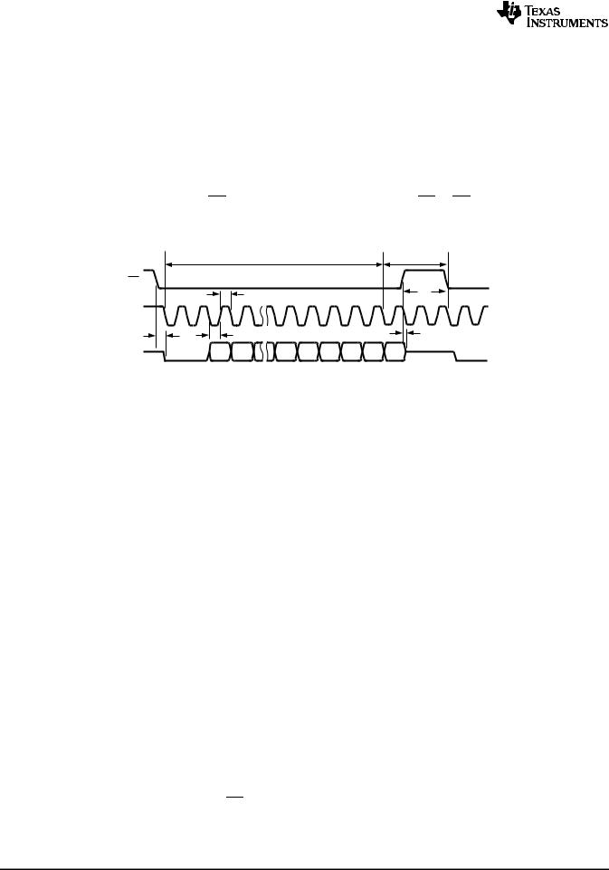
The data output format of the ADC141S626 is two’s complement as shown in Figure 38. This figure indicates the ideal output code for a given input voltage and does not include the effects of offset, gain error, linearity errors, or noise. Each data output bit is output on the falling edges of SCLK. The 1st and 2nd SCLK falling edges clock out leading zeros while the 3rd to 16th SCLK falling edges clock out the conversion result, MSB first.
While most receiving systems will capture the digital output bits on the rising edges of SCLK, the falling edges of SCLK may be used to capture the conversion result if the minimum hold time for DOUT is acceptable. See Figure 6 for DOUT hold (tDH) and access (tDA) times.
DOUT is enabled on the falling edge of CS and disabled on the rising edge of CS. If CS is raised prior to the 16th falling edge of SCLK, the current conversion is aborted and DOUT will go into its high impedance state. A new
conversion will begin when CS is driven LOW.
tCONV (Power-Up)
CS
tACQ (Power-Down)
|
|
|
|
|
tCH |
|
|
|
|
|
|
|
tCS |
|
|
1 |
|
2 |
3 |
4 |
5 |
11 |
12 |
13 |
14 |
15 |
16 |
17 |
18 |
1 |
2 |
SCLK |
|
|
|
|
|
|
|
|
|
|
|
|
|
|
|
|
|
tEN |
|
tCL |
|
|
|
|
|
|
|
|
tDIS |
|
|
|
|
|
|
|
|
|
|
|
|
|
|
|
|
||
D` |
0 |
0 |
DB13 DB12 |
DB5 |
DB4 |
DB3 |
DB2 |
DB1 |
DB0 |
|
|
0 |
0 |
||
Figure 43. ADC141S626 Single Conversion Timing Diagram
Applications Information
OPERATING CONDITIONS
We recommend that the following conditions be observed for operation of the ADC141S626:
−40°C ≤ TA ≤ +85°C
+2.7V ≤ VA ≤ +5.5V
+2.7V ≤ VIO ≤ +5.5V
1V ≤ VREF ≤ VA
0.9 MHz ≤ fSCLK ≤ 4.5 MHz
VCM: See Input Common Mode Voltage
POWER CONSUMPTION
The architecture, design, and fabrication process allow the ADC141S626 to operate at conversion rates up to 250 kSPS while consuming very little power. The ADC141S626 consumes the least amount of power while operating in acquisition (power-down) mode. For applications where power consumption is critical, the ADC141S626 should be operated in acquisition mode as often as the application will tolerate. To further reduce power consumption, stop the SCLK while CS is high.
Short Cycling
Short cycling refers to the process of halting a conversion after the last needed bit is outputted. Short cycling can be used to lower the power consumption in those applications that do not need a full 14-bit resolution, or where an analog signal is being monitored until some condition occurs. In some circumstances, the conversion could be terminated after the first few bits. This will lower power consumption in the converter since the ADC141S626 spends more time in acquisition mode and less time in conversion mode.
Short cycling is accomplished by pulling CS high after the last required bit is received from the ADC141S626 output. This is possible because the ADC141S626 places the latest converted data bit on DOUT as it is generated. If only 10-bits of the conversion result are needed, for example, the conversion can be terminated by pulling CS high after the 10th bit has been clocked out.
18 |
Submit Documentation Feedback |
Copyright © 2007–2013, Texas Instruments Incorporated |
Product Folder Links: ADC141S626

ADC141S626
www.ti.com |
SNAS434B –NOVEMBER 2007 –REVISED MARCH 2013 |
Burst Mode Operation
Normal operation of the ADC141S626 requires the SCLK frequency to be 18 times the sample rate and the CS rate to be the same as the sample rate. However, in order to minimize power consumption in applications requiring sample rates below 250 kSPS, the ADC141S626 should be run with an SCLK frequency of 4.5 MHz and a CS rate as slow as the system requires. When this is accomplished, the ADC141S626 is operating in burst mode. The ADC141S626 enters into acquisition mode at the end of each conversion, minimizing power consumption. This causes the converter to spend the longest possible time in acquisition mode. Since power consumption scales directly with conversion rate, minimizing power consumption requires determining the lowest conversion rate that will satisfy the requirements of the system.
PCB LAYOUT AND CIRCUIT CONSIDERATIONS
For best performance, care should be taken with the physical layout of the printed circuit board. This is especially true with a low VREF or when the conversion rate is high. At high clock rates there is less time for settling, so it is important that any noise settles out before the conversion begins.
Analog and Digital Power Supplies
Any ADC architecture is sensitive to spikes on the power supply, reference, and ground pins. These spikes may originate from switching power supplies, digital logic, high power devices, and other sources. Power to the ADC141S626 should be clean and well bypassed. A 0.1 µF ceramic bypass capacitor and a 1 µF to 10 µF capacitor should be used to bypass the ADC141S626 supply, with the 0.1 µF capacitor placed as close to the ADC141S626 package as possible.
Since the ADC141S626 has both the VA and VIO pins, the user has three options on how to connect these pins. The first option is to tie VA and VIO together and power them with the same power supply. This is the most cost effective way of powering the ADC141S626 but is also the least ideal. As stated previously, noise from VIO can couple into VA and adversely affect performance. The other two options involve the user powering VA and VIO with separate supply voltages. These supply voltages can have the same amplitude or they can be different. They may be set independent of each other to any value between 2.7V and 5.5V.
Best performance will typically be achieved with VA operating at 5V and VIO at 3V. Operating VA at 5V offers the best linearity and dynamic performance when VREF is also set to 5V; while operating VIO at 3V reduces the power consumption of the digital logic. Operating the digital interface at 3V also has the added benefit of decreasing the noise created by charging and discharging the capacitance of the digital interface pins.
Voltage Reference
The reference source must have a low output impedance and needs to be bypassed with a minimum capacitor value of 0.1 µF. A larger capacitor value of 1 µF to 10 µF placed in parallel with the 0.1 µF is preferred. While the ADC141S626 draws very little current from the reference on average, there are higher instantaneous current spikes at the reference.
VREF of the ADC141S626, like all A/D converters, does not reject noise or voltage variations. Keep this in mind if VREF is derived from the power supply. Any noise and/or ripple from the supply that is not rejected by the external reference circuitry will appear in the digital results. The use of an active reference source is recommended. The LM4040 and LM4050 shunt reference families and the LM4132 and LM4140 series reference families are excellent choices for a reference source.
PCB Layout
Capacitive coupling between the noisy digital circuitry and the sensitive analog circuitry can lead to poor performance. The solution is to keep the analog circuitry separated from the digital circuitry and the clock line as short as possible. Digital circuits create substantial supply and ground current transients. The logic noise generated could have significant impact upon system noise performance. To avoid performance degradation of the ADC141S626 due to supply noise, avoid using the same supply for the VA and VREF of the ADC141S626 that is used for digital circuitry on the board.
Copyright © 2007–2013, Texas Instruments Incorporated |
Submit Documentation Feedback |
19 |
Product Folder Links: ADC141S626

ADC141S626
SNAS434B –NOVEMBER 2007 –REVISED MARCH 2013 |
www.ti.com |
Generally, analog and digital lines should cross each other at 90° to avoid crosstalk. However, to maximize accuracy in high resolution systems, avoid crossing analog and digital lines altogether. It is important to keep clock lines as short as possible and isolated from ALL other lines, including other digital lines. In addition, the clock line should also be treated as a transmission line and be properly terminated. The analog input should be isolated from noisy signal traces to avoid coupling of spurious signals into the input. Any external component (e.g., a filter capacitor) connected between the converter'sinput pins and ground or to the reference input pin and ground should be connected to a very clean point in the ground plane.
A single, uniform ground plane and the use of split power planes are recommended. The power planes should be located within the same board layer. All analog circuitry (input amplifiers, filters, reference components, etc.) should be placed over the analog power plane. All digital circuitry should be placed over the digital power plane. Furthermore, the GND pins on the ADC141S626 and all the components in the reference circuitry and input signal chain that are connected to ground should be connected to the ground plane at a quiet point. Avoid connecting these points too close to the ground point of a microprocessor, microcontroller, digital signal processor, or other high power digital device.
20 |
Submit Documentation Feedback |
Copyright © 2007–2013, Texas Instruments Incorporated |
Product Folder Links: ADC141S626
ADC141S626
www.ti.com |
SNAS434B –NOVEMBER 2007 –REVISED MARCH 2013 |
APPLICATION CIRCUITS
The following figures are examples of the ADC141S626 in typical application circuits. These circuits are basic and will generally require modification for specific circumstances.
Data Acquisition
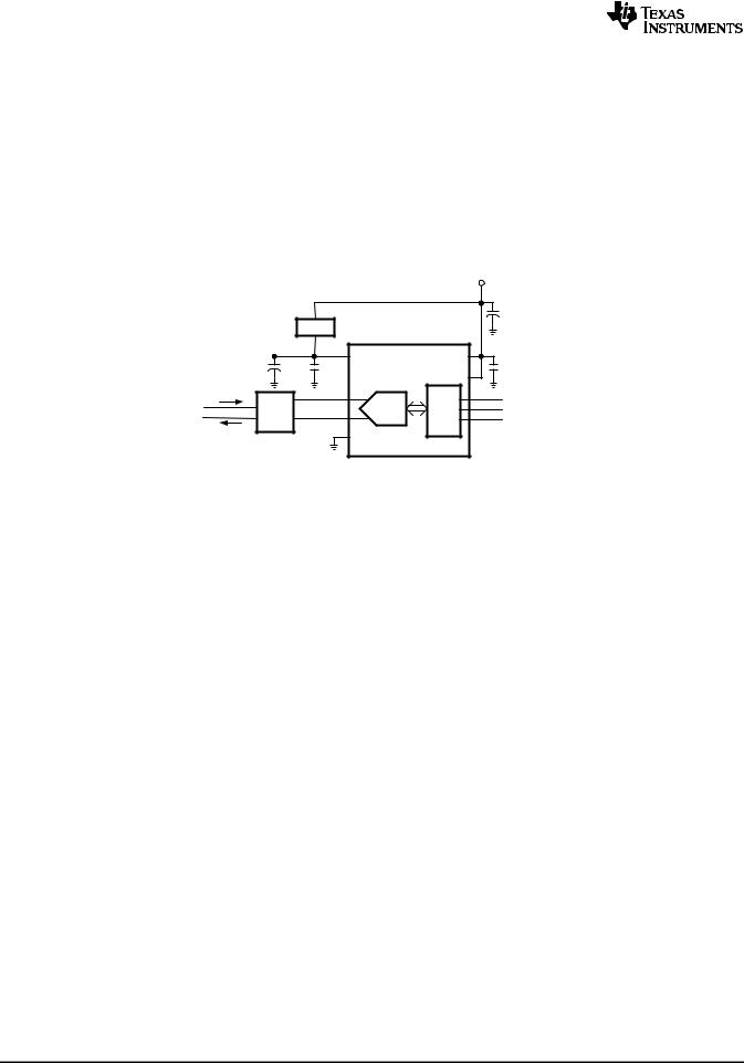
Figure 44 shows a typical connection diagram for the ADC141S626 operating at VA of +5V. VREF is connected to a 4.1V shunt reference, the LM4040-4.1, to define the analog input range of the ADC141S626 independent of
supply variation on the +5V supply line. The VREF pin should be de-coupled to the ground plane by a 0.1 µF ceramic capacitor and a tantalum capacitor of 10 µF. It is important that the 0.1 µF capacitor be placed as close
as possible to the VREF pin while the placement of the tantalum capacitor is less critical. It is also recommended that the VA and VIO pins of the ADC141S626 be de-coupled to ground by a 0.1 µF ceramic capacitor in parallel with a 10 µF tantalum capacitor.
+5V
100: |
|
ADC141S626 |
|
|
|
||
|
+ |
VREF |
VA |
LM4040-4.1 |
10 PF |
0.1 PF |
0.1 PF |
|
|
VIO |
|
|
|
|
|
+IN |
SCLK |
-IN |
DOUT |
GND |
CSB |
+ 10 PF
Controller
Figure 44. Low cost, low power Data Acquisition System
Bridge Sensor Application
Figure 45 shows an example of interfacing a bridge sensor to the ADC141S626. The application assumes that the bridge sensor requires buffering and amplification to fully utilize the dynamic range of the ADC and thus optimize the performance of the entire signal path. The amplification stage consists of the LMP7702, a dual precision amplifier, and some gain setting passive components. The amplification stage offers the benefit of high input impedance and high amplification capability. On the other hand, it offers no common-mode rejection of common-mode noise or DC-voltage coming from the bridge sensor.
The DAC081S101, a digital-to-analog converter (DAC), is used to bias the bridge sensor. The DAC provides a mean for dynamically adjusting the gain of the bridge sensor relative to actual maximum and minimum output conditions. Another option for biasing the bridge sensor would be powering it from the same +5V power supply voltage as the VA pin on the ADC141S626. This option has the benefit of providing the ideal common-mode input voltage for the ADC141S626 while keeping design complexity and cost to a minimum. However, any fluctuation in the +5V supply will still be visible in the converted result. The LM4132-4.1, a 4.1V series reference, is used as the reference voltage in the application. The ADC141S626, DAC081S101, and the LM4132-4.1 are all powered from the same +5V voltage source.
|
|
|
|
|
|
|
|
|
|
|
|
|
|
|
|
|
|
|
|
|
+5V |
|
|||
|
|
|
|
|
|
|
|
LMP7702 |
|
|
|
|
|
|
|
|
|
|
|
|
|
SYNCB |
|
||
|
|
|
|
|
|
|
|
|
|
|
|
|
|
|
|
|
|
|
|
|
|
||||
|
|
|
|
|
|
|
|
|
|
|
|
|
|
|
|
|
|
|
|
|
|
|
|
||
|
|
|
|
|
|
|
|
|
|
|
|
|
|
|
|
|
|
|
|
|
DAC081S101 |
|
|||
|
|
|
|
|
|
|
+ |
|
470 pF |
|
|
|
|
|
|
|
|
|
|
|
DIN |
|
|
||
|
|
|
|
|
|
|
- |
|
180: |
|
|
|
+5V +5V |
|
|
SCLK |
Micro- |
||||||||
|
|
|
|
|
|
|
|
100 k: |
|
|
|
|
|
|
|
|
|
|
|
|
|
|
Controller |
||
|
|
|
|
|
|
||||||||||||||||||||
|
|
|
|
|
|
|
|
|
|
|
|
|
|
|
|||||||||||
|
|
|
VA |
VIO |
|
SCLK |
|
|
2 k: |
|
ADC141S626 |
|
|||
|
|
DOUT |
|
||||
|
|
|
REF |
|
|
||
|
|
|
|
|
|
||
|
|
100 k: |
180: |
|
CSB |
|
|
|
|
|
|
|
|||
|
- |
|
|
|
|
||
|
|
|
|
|
LM4132-4.1 |
+5V |
|
|
+ |
AV = 100 V/V |
|
|
|||
Bridge |
|
+ |
|
|
+ |
||
|
|
0.1 PF |
4.7 PF |
||||
Sensor |
|
|
|
4.7 PF |
|||
Figure 45. Interfacing the ADC141S626 to a Bridge Sensor
Copyright © 2007–2013, Texas Instruments Incorporated |
Submit Documentation Feedback |
21 |
Product Folder Links: ADC141S626
ADC141S626
SNAS434B –NOVEMBER 2007 –REVISED MARCH 2013 |
www.ti.com |
Current Sensing Application
Figure 46 shows an example of interfacing a current transducer to the ADC141S626. The current transducer converts an input current into a voltage that is converted by the ADC. Since the output voltage of the current transducer is single-ended and centered around a common-mode voltage (VCM) of 2.5V, the ADC141S626 is configured with the output of the transducer driving the non-inverting input and VCM of the transducer driving the inverting input. The output of the transducer has an output range of ±2V around VCM of 2.5V. As a result, a series reference voltage of 2.0V is connected to the ADC141S626. This will allow all of the codes of the ADC141S626 to be available for the application. This configuration of the ADC141S626 is referred to as a single-ended application of a differential ADC. All of the elements in the application are conveniently powered by the same +5V power supply, keeping circuit complexity and cost to a minimum.
|
|
|
|
|
|
|
+5V |
|
|
|
|
|
|
|
+ 10 PF |
|
LM4132-2.0 |
|
|
|
|
|
|
|
+ |
0.1 PF |
VREF |
ADC141S626 |
VA |
0.1 PF |
|
|
10 PF |
|
|
|
|
||
|
|
|
|
|
|
VIO |
|
IIN |
OUT |
2.5V + 2.0V |
|
|
|
|
SCLK |
|
|
|
Serial |
|
DOUT |
||
+5V |
|
|
ADC |
|
|||
IIN |
2.5V |
|
Interface |
CSB |
|||
IOUT VCM |
- |
|
|||||
|
|
|
|
|
|||
IOUT |
GND |
|
|
|
|
|
|
LTSR-1513¶V |
|
GND |
|
|
|
|
|
|
|
|
|
|
|
||
Figure 46. Interfacing the ADC141S626 to a Current Transducer
22 |
Submit Documentation Feedback |
Copyright © 2007–2013, Texas Instruments Incorporated |
Product Folder Links: ADC141S626