

ADC141S626
www.ti.com |
SNAS434B –NOVEMBER 2007 –REVISED MARCH 2013 |
ANALOG SIGNAL INPUTS
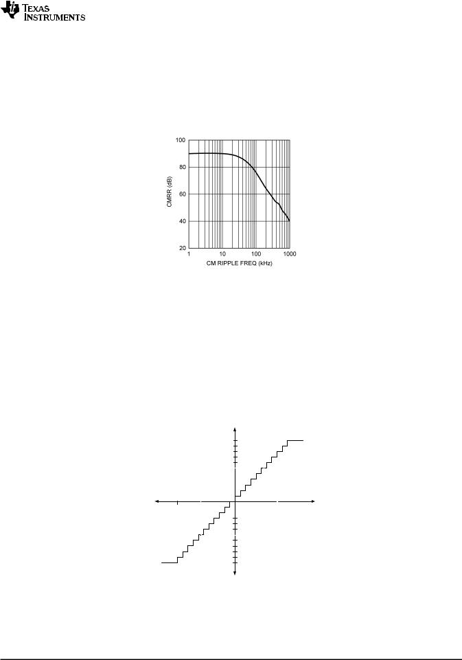
The ADC141S626 has a differential input where the effective input voltage that is digitized is (+IN) − (−IN). By using this differential input, small signals common to both inputs are rejected. As shown in Figure 37, noise is immune at low frequencies where the common-mode rejection ratio (CMRR) is 90 dB. As the frequency increases to 1 MHz, the CMRR rolls off to 40 dB . In general, operation with a fully differential input signal or voltage will provide better performance than with a single-ended input. However, if desired, the ADC141S626 can be presented with a single-ended input.
Figure 37. Analog Input CMRR vs. Frequency
The current required to recharge the input sampling capacitor will cause voltage spikes at +IN and −IN. Do not try to filter out these noise spikes. Rather, ensure that the transient settles out during the acquisition period.
Differential Input Operation
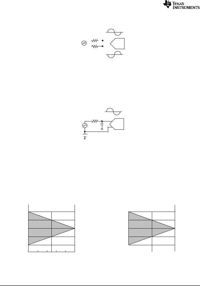
As shown in Figure 38 for a fully differential input signal, a positive full scale output code (01 1111 1111 1111b or 1FFFh or 8191d) will be obtained when (+IN) − (−IN) is greater than or equal to (VREF − 1 LSB). A negative full scale code (10 0000 0000 0000b or 2000h or -8192d) will be obtained when (+IN) − (−IN) is less than or equal to (−VREF + 1 LSB). This ignores gain, offset and linearity errors, which will affect the exact differential input voltage that will determine any given output code. Both inputs should be biased at a common mode voltage (VCM), which will be thoroughly discussed in Input Common Mode Voltage . Figure 39 shows the ADC141S626 being driven by a full-scale differential source.
ADC Output Code
| - VREF +1LSB
|
01 1111 1111 1111b
| |
|
|
| |
|
|
|
|||||||
|
|
|
|
|
|
|
|
|
|
|
|
||
|
|
|
|
|
|
|
|
|
|
|
|
||
|
|
|
|
|
|
|
|
|
|
|
|||
-1 LSB |
|
|
|
|
|
|
|
||||||
|
|
|
|
|
|
||||||||
|
|
|
|
|
|
|
|
|
|||||
|
|
|
|
00 |
|
0000 0000 0000b |
| |
|
|
||||
|
|
|
|
+1 |
|
+VREF ±1LSB |
|||||||
|
|
|
|
|
|
|
LSB |
|
|
|
|
||
|
|
|
|
|
|
|
|
|
|
|
|||
|
10 0000 0000 0000b
Analog Input
Figure 38. ADC Output vs. Input for a Differential Input Operation
Copyright © 2007–2013, Texas Instruments Incorporated |
Submit Documentation Feedback |
15 |
Product Folder Links: ADC141S626
ADC141S626
SNAS434B –NOVEMBER 2007 –REVISED MARCH 2013 |
|
|
|
|
|
|
|
www.ti.com |
|||||||
|
|
|
|
VCM + |
|
VREF |
|
||||||||
|
|
|
|
|
2 |
|
|
|
|||||||
|
|
|
|
|
|
|
|
|
|
|
|||||
|
|
|
|
|
|
|
|
VCM |
|
||||||
|
|
|
|
VCM - |
VREF |
|
|
|
|||||||
|
|
|
|
|
|
|
|||||||||
|
|
|
|
RS |
2 |
|
|
|
|||||||
|
|
|
|
|
|
|
|
|
|
|
|||||
VREF |
|
|
|
|
|
|
|
|
|
|
|
|
+ |
||
SRC |
|
|
|
|
|
|
|
|
|
|
|
CS |
ADC141S626 |
||
|
|
|
|
|
|
|
|
|
|
|
|
|
|
|
- |
|
|
|
|
RS VCM + |
|
|
VREF |
|
|||||||
|
|
|
|
|
|
|
|
||||||||
|
|
|
|
2 |
|
|
|
||||||||
|
|
|
|
|
|
|
|
VCM |
|
||||||
|
|
|
|
VCM - |
VREF |
|
|||||||||
|
|
|
|
|
|
|
|
2 |
|
|
|
||||
Figure 39. Differential Input
Single-Ended Input Operation
For single-ended operation, the non-inverting input (+IN) of the ADC141S626 can be driven with a signal that has a peak-to-peak range that is equal to or less than (2 x VREF). The inverting input (−IN) should be biased at a stable VCM that is halfway between these maximum and minimum values. In order to utilize the entire dynamic range of the ADC141S626, VREF is limited to VA / 2. This allows +IN a maximum swing range of ground to VA. Figure 40 shows the ADC141S626 being driven by a full-scale single-ended source.
VCM + VREF
VCM
VCM - VREF
RS
VREF |
|
+ |
|
CS |
ADC141S626 |
||
SRC |
|||
|
- |
||
|
|
VCM 
Figure 40. Single-Ended Input
Since the design of the ADC141S626 is optimized for a differential input, the performance degrades slightly when driven with a single-ended input. Linearity characteristics such as INL and DNL typically degrade by 0.1 LSB and dynamic characteristics such as SINAD typically degrade by 2 dB. Note that single-ended operation should only be used if the performance degradation (compared with differential operation) is acceptable.
Input Common Mode Voltage
The allowable input common mode voltage (VCM) range depends upon VA and VREF used for the ADC141S626. The ranges of VCM are depicted in Figure 41 and Figure 42. Note that these figures only apply to a VA of 5V. Equations for calculating the minimum and maximum VCM for differential and single-ended operations are shown in Table 1.
|
6 |
|
Differential Input |
|
|
|
|
(V) |
5 |
|
|
|
|
||
|
|
|
|
VOLTAGE |
3.75 |
|
|
|
|
||
|
|
|
|
MODE- |
2.5 |
|
|
|
|
||
|
|
|
|
COMMON |
0 |
|
|
|
|
||
|
1.25 |
|
|
-1 0.0 1.0 2.0 2.5 3.0 4.0 5.0
VREF (V)
Figure 41. VCM range for Differential Input operation
|
6 |
|
Single-Ended Input |
|
|
||||
|
|
|
|
|
|||||
(V) |
5 |
|
|
|
|
|
|
|
|
|
|
|
|
|
|
|
|
||
|
|
|
|
|
|
|
|
|
|
VOLTAGE |
3.75 |
|
|
|
|
|
|
|
|
|
|
|
|
|
|
|
|
||
|
|
|
|
|
|
|
|
|
|
MODE- |
2.5 |
|
|
|
|
|
|
|
|
|
|
|
|
|
|
|
|
||
|
|
|
|
|
|
|
|
|
|
COMMON |
0 |
|
|
|
|
|
|
|
|
|
|
|
|
|
|
|
|
||
|
1.25 |
|
|
|
|
|
|
|
|
|
-1 |
|
|
|
|
|
|
|
|
|
|
|
|
|
|
|
|
|
|
|
|
|
|
|
|
|
|
|
|
|
|
|
|
1.25 |
|
|
|
|
|
|
0.0 |
0.75 |
1.75 |
2.5 |
|||||
VREF (V)
Figure 42. VCM range for single-ended operation
16 |
Submit Documentation Feedback |
Copyright © 2007–2013, Texas Instruments Incorporated |
Product Folder Links: ADC141S626