

ADC141S626
SNAS434B –NOVEMBER 2007 –REVISED MARCH 2013 |
www.ti.com |
ADC141S626 Timing Specifications(1)
The following specifications apply for VA = VIO = VREF= +2.7V to 5.5V and fSCLK = 0.9 to 4.5 MHz, CL = 25 pF, Boldface limits apply for TA = TMIN to TMAX: all other limits TA = 25°C.
Symbol |
|
|
|
|
|
|
Parameter |
Conditions |
Typical |
Limits |
Units |
||
|
|
|
|
|
|
|
|
|
|
|
|
|
|
|
|
|
|
|
|
|
|
|
|
|
3 |
6 |
ns (min) |
tCSS |
|
CS Setup Time prior to an SCLK rising edge |
|
||||||||||
|
|
|
|
|
|||||||||
|
1/fSCLK - 3 |
1/fSCLK - 6 |
ns (max) |
||||||||||
|
|
|
|
|
|
|
|
|
|
|
|||
tDH |
|
DOUT Hold Time after an SCLK falling edge |
|
10 |
6 |
ns (min) |
|||||||
tDA |
|
DOUT Access Time after an SCLK falling edge |
|
28 |
40 |
ns (max) |
|||||||
t |
|
D |
|
|
Disable Time after the rising edge of |
|
(2) |
|
10 |
20 |
ns (max) |
||
OUT |
CS |
|
|||||||||||
DIS |
|
|
|
|
|
|
|
|
|
|
|
||
tCS |
|
Minimum |
|
Pulse Width |
|
5 |
20 |
ns (min) |
|||||
CS |
|
||||||||||||
tEN |
|
DOUT Enable Time after the falling edge of |
|
|
|
32 |
51 |
ns (max) |
|||||
CS |
|
||||||||||||
tCH |
|
SCLK High Time |
|
67 |
89 |
ns (min) |
|||||||
tCL |
|
SCLK Low Time |
|
67 |
89 |
ns (min) |
|||||||
tr |
|
DOUT Rise Time |
|
7 |
|
ns |
|||||||
tf |
|
DOUT Fall Time |
|
7 |
|
ns |
|||||||
(1)Typical values are at TJ = 25°C and represent most likely parametric norms. Test limits are guaranteed to TI's AOQL (Average Outgoing Quality Level).
(2)tDIS is the time for DOUT to change 10% while being loaded by the Timing Test Circuit.
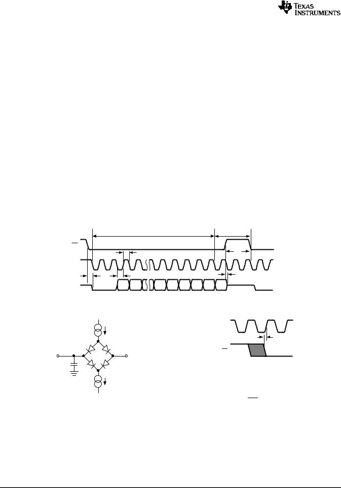
Timing Diagrams
tCONV (Power-Up)
CS
tACQ (Power-Down)
|
|
|
tCH |
|
|
|
|
|
|
|
tCS |
|
|
|
|
|
|
|
|
|
|
|
|
17 |
18 |
1 |
2 |
||
1 |
2 |
3 |
4 |
5 |
11 |
12 |
13 |
14 |
15 |
16 |
||||
SCLK |
|
|
|
|
|
|
|
|
|
|
|
|
|
|
|
tEN |
|
tCL |
|
|
|
|
|
|
|
|
tDIS |
|
|
|
|
|
|
|
|
|
|
|
|
|
|
|
||
D` |
0 |
0 DB13 DB12 |
|
DB5 DB4 DB3 DB2 DB1 DB0 |
|
0 |
0 |
|||||||
Figure 1. ADC141S626 Single Conversion Timing Diagram |
||||||||||||||
2 mA |
|
IOL |
|
|
|
|
|
|
|
SCLK |
|
1 |
2 |
|
|
|
|
|
|
|
|
|
|
|
|
|
|
||
|
|
|
|
|
|
|
|
|
|
|
|
|
|
tCSS |
TO OUTPUT |
|
|
|
|
|
|
|
|
|
|
CS |
|
|
|
|
|
1.6V |
|
|
|
|
|
|
|
|
|
|
|
|
PIN |
|
|
|
|
|
|
|
|
|
|
|
|
|
|
|
|
|
|
|
|
|
|
|
|
|
|
|
|
|
CL |
|
|
|
|
|
|
|
|
|
|
|
|
|
|
25 pF |
|
|
|
|
|
|
|
|
|
|
|
|
|
|
2 mA |
|
IOH |
|
|
|
|
|
|
|
|
|
|
|
|
Figure 2. Timing Test Circuit |
|
|
|
|
|
Figure 3. Valid CS Assertion Times |
||||||||
6 |
Submit Documentation Feedback |
Copyright © 2007–2013, Texas Instruments Incorporated |
Product Folder Links: ADC141S626
|
|
|
|
|
|
|
|
|
|
|
|
|
|
|
|
|
|
|
|
|
|
|
|
|
|
|
|
|
|
|
|
|
|
|
|
|
|
|
|
|
|
|
|
ADC141S626 |
www.ti.com |
|
|
|
|
|
|
|
|
SNAS434B –NOVEMBER 2007 –REVISED MARCH 2013 |
|||||||||||||||||||||||||||||||||||
|
|
|
|
|
|
|
|
|
|
|
|
|
|
|
|
|
|
0.9 x VIO |
|
|
|
|
|
|
|
|
|
|
|
|
|
|
|
|
|
|
|
|
||||||
|
|
|
|
|
|
|
|
|
|
|
|
|
|
|
|
|
|
|
|
|
|
|
|
|
|
|
|
|
|
|
|
VIH |
||||||||||||
DOUT |
|
|
tr |
|
|
|
|
|
|
|
|
|
|
|
|
0.1 x VIO |
CS |
|
|
|
|
|||||||||||||||||||||||
|
|
|
|
|
|
|
|
|
|
|
|
|
|
|
|
|
|
|
|
|
|
|
|
|
|
|
|
|
|
|||||||||||||||
|
|
|
|
|
|
|
|
|
|
|
|
|
|
|
|
tf |
|
|
|
|
|
DOUT |
|
|
|
|
|
|
|
|
|
|
|
90%90% |
|
|
||||||||
|
|
|
|
|
|
|
|
|
|
|
|
|
|
|
|
|
|
|
|
|
|
|
|
|
|
|
|
|
|
|
|
|
|
|||||||||||
|
|
|
|
|
|
|
|
|
|
|
|
|
|
|
|
|
|
|
|
|
|
|||||||||||||||||||||||
|
|
|
|
|
|
|
|
|
|
|
|
|
|
|
|
|
|
|
|
|
|
|
|
|
|
|
|
|
|
|
|
|
|
|
|
|||||||||
|
|
|
|
|
|
|
|
|
|
|
|
|
|
|
|
|
|
|
|
|
|
|
|
|
|
|
|
|
|
|
|
|
|
|
|
|||||||||
|
|
|
|
|
|
|
|
|
|
|
|
|
|
|
|
|
|
|
|
|
|
|
|
|
|
|
|
|
|
|
|
|
|
|
|
|
|
|
|
|
|
|||
|
|
|
|
|
|
|
|
|
|
|
|
|
|
|
|
|
|
|
|
|
|
|
|
|
|
|
|
|
|
|
|
10% |
|
|
|
|
|
|
|
|
|
|
|
|
|
|
|
|
|
|
|
|
|
|
|
|
|
|
|
|
|
|
|
|
|
|
|
|
|
|
|
|
|
|
|
|
tDIS |
|
|
|
|||||||||
|
|
|
|
|
|
|
|
|
|
|
|
|
|
|
|
|
|
|
|
|
|
|
|
|
|
|
|
|
|
|
|
|
|
|
|
|
|
|
|
|||||
|
|
|
|
|
|
|
|
|
|
|
|
|
|
|
|
|
|
|
|
|
|
|
|
|
DOUT |
90% |
|
|
|
|
|
|
|
|
|
|
|
|||||||
|
|
|
|
|
|
|
|
|
|
|
|
|
|
|
|
|
|
|
|
|
|
|
|
|
|
|
|
|
|
|
|
|
|
|
|
|||||||||
|
|
|
|
|
|
|
|
|
|
|
|
|
|
|
|
|
|
|
|
|
|
|
|
|
|
|
|
|
|
|
|
|
|
|
10%10% |
|
|
|||||||
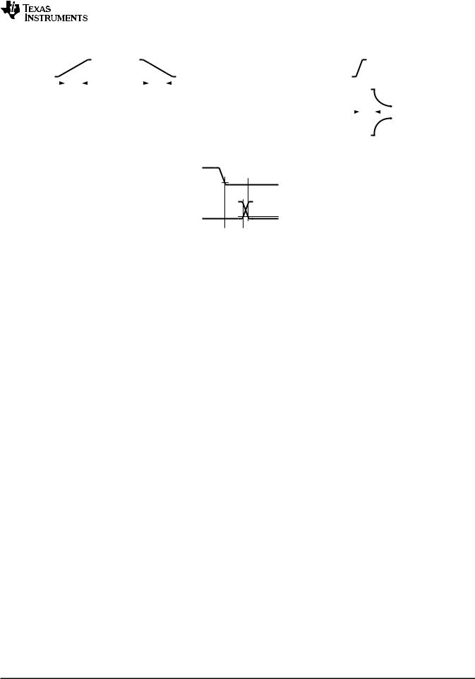
Figure 4. DOUT Rise and Fall Times |
Figure 5. Voltage Waveform for tDIS |
|||||||||||||||||||||||||||||||||||||||||||
SCLK
VIL

 tDA
tDA

 2.3V
2.3V
DOUT
0.7V
tDH 

Figure 6. DOUT Hold and Access Times
Specification Definitions
APERTURE DELAY is the time between the first falling edge of SCLK and the time when the input signal is sampled for conversion.
COMMON MODE REJECTION RATIO (CMRR) is a measure of how well in-phase signals common to both input pins are rejected.
To calculate CMRR, the change in output offset is measured while the common mode input voltage is changed from 2V to 3V.
CMRR = 20 LOG ( Common Input / Output Offset) |
(1) |
CONVERSION TIME is the time required, after the input voltage is acquired, for the ADC to convert the input voltage to a digital word.
DIFFERENTIAL NON-LINEARITY (DNL) is the measure of the maximum deviation from the ideal step size of 1 LSB.
DUTY CYCLE is the ratio of the time that a repetitive digital waveform is high to the total time of one period. The specification here refers to the SCLK.
EFFECTIVE NUMBER OF BITS (ENOB, or EFFECTIVE BITS) is another method of specifying Signal-to-Noise and Distortion or SINAD. ENOB is defined as (SINAD − 1.76) / 6.02 and says that the converter is equivalent to a perfect ADC of this (ENOB) number of bits.
FULL POWER BANDWIDTH is a measure of the frequency at which the reconstructed output fundamental drops 3 dB below its low frequency value for a full scale input.
GAIN ERROR is the deviation from the ideal slope of the transfer function. It is the difference between Positive Full-Scale Error and Negative Full-Scale Error and can be calculated as:
Gain Error = Positive Full-Scale Error − Negative Full-Scale Error |
(2) |
INTEGRAL NON-LINEARITY (INL) is a measure of the deviation of each individual code from a line drawn from ½ LSB below the first code transition through ½ LSB above the last code transition. The deviation of any given code from this straight line is measured from the center of that code value.
MISSING CODES are those output codes that will never appear at the ADC outputs. The ADC141S626 is guaranteed not to have any missing codes.
NEGATIVE FULL-SCALE ERROR is the difference between the differential input voltage at which the output code transitions from negative full scale to the next code and −VREF + 1 LSB
NEGATIVE GAIN ERROR is the difference between the negative full-scale error and the offset error.
OFFSET ERROR is the difference between the differential input voltage at which the output code transitions from code 0000h to 0001h and 1 LSB.
Copyright © 2007–2013, Texas Instruments Incorporated |
Submit Documentation Feedback |
7 |
Product Folder Links: ADC141S626

ADC141S626
SNAS434B –NOVEMBER 2007 –REVISED MARCH 2013 |
www.ti.com |
POSITIVE FULL-SCALE ERROR is the difference between the differential input voltage at which the output code transitions to positive full scale and VREF minus 1 LSB.
POSITIVE GAIN ERROR is the difference between the positive full-scale error and the offset error.
POWER SUPPLY REJECTION RATIO (PSRR) is a measure of how well a change in the analog supply voltage is rejected. PSRR is calculated from the ratio of the change in offset error for a given change in supply voltage, expressed in dB. For the ADC141S626, VA is changed from 4.5V to 5.5V.
PSRR = 20 LOG ( Output Offset / VA) |
(3) |
SIGNAL TO NOISE RATIO (SNR) is the ratio, expressed in dB, of the rms value of the input signal to the rms value of the sum of all other spectral components below one-half the sampling frequency, not including harmonics or d.c.
SIGNAL TO NOISE PLUS DISTORTION (S/N+D or SINAD) Is the ratio, expressed in dB, of the rms value of the input signal to the rms value of all of the other spectral components below one-half the sampling frequency, including harmonics but excluding d.c.
SPURIOUS FREE DYNAMIC RANGE (SFDR) is the difference, expressed in dB, between the desired signal amplitude to the amplitude of the peak spurious spectral component below one-half the sampling frequency, where a spurious spectral component is any signal present in the output spectrum that is not present at the input and may or may not be a harmonic.
TOTAL HARMONIC DISTORTION (THD) is the ratio of the rms total of the first five harmonic components at the output to the rms level of the input signal frequency as seen at the output, expressed in dB. THD is calculated as
THD = 20 ‡ log10 |
Af 22 + + Af 62 |
Af12 |
(4)
where Af1 is the RMS power of the input frequency at the output and Af2 through Af6 are the RMS power in the first 5 harmonic frequencies.
THROUGHPUT TIME is the minimum time required between the start of two successive conversion.
8 |
Submit Documentation Feedback |
Copyright © 2007–2013, Texas Instruments Incorporated |
Product Folder Links: ADC141S626