

MCP111/112
4.0APPLICATION INFORMATION
For many of today’s microcontroller applications, care must be taken to prevent low-power conditions that can cause many different system problems. The most common causes are brown-out conditions, where the system supply drops below the operating level momentarily. The second most common cause is when a slowly decaying power supply causes the microcontroller to begin executing instructions without sufficient voltage to sustain SRAM, thus producing indeterminate results. Figure 4-1 shows a typical application circuit.
VDD |
|
|
|
|
|
|
|
|
|
|
|
|
|
|
|
|
|
|
|
|
|
|
|
|
|
|
|||||||
|
|
|
|
|
|
3 |
|
|
|
|
|
|
|
|
|
|
|
|
|
|
|
|
|||||||||||
|
|
|
|
|
|
|
|
|
|
|
|
|
|
|
|
|
|
|
|
|
VDD |
|
|||||||||||
|
|
|
|
|
|
|
|
|
|
|
|
|
|
|
|
|
|
|
|
|
|
|
|
|
|
||||||||
0.1 |
|
|
|
|
|
|
|
|
|
|
VDD |
|
|
|
|
|
RPU |
|
PICmicro® |
|
|||||||||||||
|
|
|
|
|
|
|
|
|
|
|
|
|
|
|
|
|
|||||||||||||||||
|
|
|
|
|
|
|
|
|
|
|
|
|
|
|
|
|
|
|
|
|
|
|
|||||||||||
µF |
|
|
|
|
|
|
|
|
MCP11X |
1 |
|
|
|
(1) |
|
Microcontroller |
|
||||||||||||||||
|
|
|
|
|
|
|
|
|
|
|
|
|
|
||||||||||||||||||||
|
|
|
|
|
|
|
|
|
|
|
|
|
|
|
VOUT |
|
|
|
|
|
|
|
|
|
|
|
|
|
|
|
|||
|
|
|
|
|
|
|
|
|
|
|
|
|
|
|
MCLR |
|
|||||||||||||||||
|
|
|
|
|
|
|
|
|
|
|
|
|
|
|
|
|
|
|
|
|
|
||||||||||||
|
|
|
|
|
|
|
|
|
|
VSS |
|
|
|
|
|
|
(Reset Input) |
|
|||||||||||||||
|
|
|
|
|
|
|
|
|
|
|
|
|
|
|
|
|
GND |
|
|||||||||||||||
|
|
|
|
|
|
|
|
|
|
|
|
|
|
2 |
|
|
|
|
|
|
|
|
|
|
|
|
|
|
|
|
|||
|
|
|
|
|
|
|
|
|
|
|
|
|
|
|
|
|
|
|
|
|
|
|
|
|
|
|
|
|
|
||||
|
|
|
|
|
|
|
|
|
|
|
|
|
|
|
|
|
|
|
|
|
|
|
|
|
|
|
|
|
|
|
|
|
|
|
|
|
|
|
|
|
|
|
|
|
|
|
|
|
|
|
|
|
|
|
|
|
|
|
|
|
|
|
|
|
|
|
|
|
|
|
|
|
|
|
|
|
|
|
|
|
|
|
|
|
|
|
|
|
|
|
|
|
|
|
|
|
|
|
|
|
|
Note 1: RPU may be required with the MCP111 due to the open-drain output. Resistor RPU is not required with the MCP112.
FIGURE 4-1: Typical Application Circuit.
4.1VTRIP Operation
The voltage trip point (VTRIP) is determined on the falling
edge of VDD. The actual voltage trip point (VTRIPAC) will be between the minimum trip point (VTRIPMIN) and the maximum trip point (VTRIPMAX). There is a hysteresis on this trip point to remove any “jitter” that would occur on
the VOUT pin when the device VDD is at the trip point.
Figure 4-2 shows the state of the VOUT pin as determined by the VDD voltage. The VTRIP specification
is for falling VDD voltages. When the VDD voltage is rising, the VOUT pin will not be driven high until VDD is at
VTRIP + VHYS.
VDD |
VTRIPMAX |
|
|
|
|
|
|
|
|
|
|
|
|
|
VTRIPAC + VHYSAC |
|
|
|
|
|
|
|
|
|
|
|
|
|
|
|
|
|
|
|
||||||||||
|
|
|
|
|
|
|
|
|
|
|
|
|
|
|
|
|
|
|
|
|
|
|
|
|
|
|
|
|
|
VTRIPAC |
||||||||||||||
|
|
|
||||||||||||||||||||||||||||||||||||||||||
|
|
|
|
|
|
|
|
|
|
|
|
|
|
|
|
|
|
|
|
|
|
|
|
|
|
|
|
|
|
|
|
|
|
|
|
|
|
|
|
|
|
|
||
|
VTRIPMIN |
|
|
|
|
|
|
|
|
|
|
|
|
|
|
|
VTRIPAC |
|
|
|||||||||||||||||||||||||
|
|
|
|
|
|
|
|
|
|
|
|
|
|
|
|
|
|
|
|
|
|
|
|
|
|
|
|
|
|
|
||||||||||||||
|
|
|
|
|
|
|
|
|
|
|
|
|
|
|
|
|
|
|
|
|
|
|
|
|
|
|
|
|
|
|
|
|
|
|
|
|
|
|
|
|
|
|
|
|
|
|
|
|
|
|
|
|
|
|
|
|
|
|
|
|
|
|
|
|
|
|
|
|
|
|
|
|
|
|
|
|
|
|
|
|
|
|
|
|
|
|
|
|
|
1V 
VOUT
< 1 V is outside the device specifications
FIGURE 4-2: VOUT Operation as Determined by the VTRIP and VHYS.
♥ 2005 Microchip Technology Inc. |
DS21889D-page 11 |
MCP111/112
4.2Negative Going VDD Transients
The minimum pulse width (time) required to cause a reset may be an important criteria in the implementation of a Power-on Reset (POR) circuit. This time is referred to as transient duration, defined as the amount of time needed for these supervisory devices to respond to a drop in VDD. The transient duration time is
dependant on the magnitude of VTRIP – VDD. Generally speaking, the transient duration decreases with
increases in VTRIP – VDD.
Figure 4-3 shows a typical transient duration vs. reset comparator overdrive for which the MCP111/112 will not generate a reset pulse. It shows that the farther below the trip point the transient pulse goes, the duration of the pulse required to cause a reset gets shorter. Figure 2-18 shows the transient response characteristics for the MCP111/112.
A 0.1 µF bypass capacitor, mounted as close as possible to the VDD pin, provides additional transient immunity (refer to Figure 4-1).
5V |
VTRIP(MAX) |
|
Voltage |
||
VTRIP(MIN) |
||
VTRIP(MIN) - VDD |
||
Supply |
tTRANS |
|
0V |
Time (µs) |
FIGURE 4-3: Example of Typical
Transient Duration Waveform.
4.3Effect of Temperature on Time-out
Period (tRPU)
The time-out period (tRPU) determines how long the device remains in the reset condition. This is affected by both VDD and temperature. The graph shown in Figures 2-22, 2-23 and 2-24 show the typical response for different VDD values and temperatures.
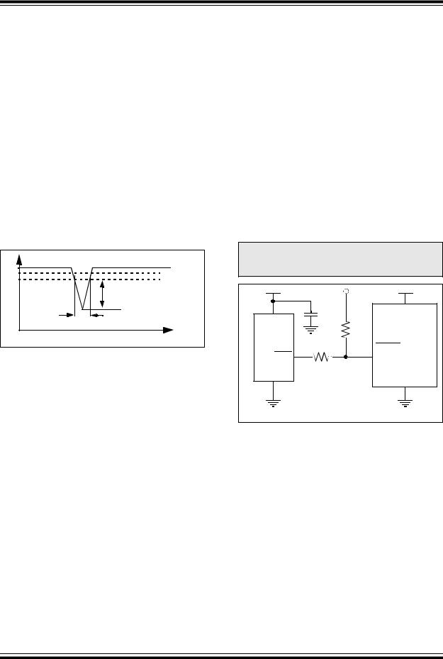
4.4Using in PICmicro® Microcontroller ICSP™ Applications (MCP111 only)
Figure 4-4 shows the typical application circuit for using the MCP111 for voltage supervisory function when the PICmicro microcontroller will be programmed via the In-Circuit Serial Programming™ (ICSP) feature. Additional information is available in TB087,
“Using Voltage Supervisors with PICmicro® Microcontroller Systems which Implement In-Circuit Serial Programming™”, DS91087.
Note: It is recommended that the current into the RST pin be current limited by a 1 kΩ resistor.
|
VDD/VPP |
0.1 µF |
VDD |
|
|
VDD |
RPU |
PICmicro® |
|
MCP111 |
MCU |
RST |
MCLR |
(reset input) |
|
1 kΩ |
(Active-Low) |
VSS |
VSS |
|
FIGURE 4-4: Typical Application Circuit for PICmicro® Microcontroller with the ICSP™ feature.
DS21889D-page 12 |
♥ 2005 Microchip Technology Inc. |