

бакМИТ_КП2015 / Компоненты по вариантам / Супервизор / MAX6802UR_xx
.pdf19-1933 Rev 2; 12/05
General Description
The MAX6800/MAX6801/MAX6802 microprocessor (µP) supervisory circuits monitor the power supplies in 2.85V to 5.0V µP and digital systems. They increase circuit reliability and reduce cost by eliminating external components and adjustments.
These devices perform a single function—they assert a reset signal whenever the VCC supply voltage declines below a preset threshold, keeping it asserted for a preset timeout period after VCC has risen above the reset threshold. The only difference among the three devices
is their output. The MAX6801 (push/pull) and MAX6802 (open-drain) have an active-low RESET output, while the
MAX6800 (push/pull) has an active-high RESET output. The MAX6800/MAX6801 are guaranteed to be in the correct state for VCC down to 0.7V. The MAX6802 is guaranteed to be in the correct state for VCC down to 1.0V.
The reset comparator in these ICs is designed to ignore fast transients on VCC. Reset thresholds are factorytrimmable between 2.63V and 4.80V, in approximately 100mV increments. These devices are available with a 1ms (min), 20ms (min), or 100ms (min) reset pulse width. Ideal for space-critical applications, the MAX6800/MAX6801/MAX6802 come packaged in a 3- pin SOT23. For a lower threshold voltage version, see the MAX6332/MAX6333/MAX6334.
Applications
Computers
Controllers
Intelligent Instruments
Critical µP/µC Power Monitoring
Portable/Battery-Powered Equipment
Automotive
Typical Operating Circuit and Pin Configuration appear at end of data sheet.
Selector Guide appears at end of data sheet.
3-Pin, Low-Power
µP Reset Circuits
Features
♦Ultra-Low 0.7V Operating Supply Voltage
♦Low 4.0µA Supply Current
♦Precision Monitoring of 2.85V to 5.0V PowerSupply Voltages
♦Reset Thresholds Available from 2.63V to 4.80V, in Approximately 100mV Increments
♦Fully Specified over Temperature
♦Three Power-On Reset Timeout Periods Available (1ms min, 20ms min, 100ms min)
♦Low Cost
♦Three Available Output Structures: Push/Pull RESET, Push/Pull RESET, Open-Drain RESET
♦Guaranteed RESET/RESET Valid to VCC = 0.7V
(MAX6800/MAX6801)
♦Power-Supply Transient Immunity
♦No External Components Required
♦3-Pin SOT23 Package
♦Pin Compatible with MAX809/MAX810, MAX6326/MAX6327/MAX6328, and MAX6346/MAX6347/MAX6348
Ordering Information
PART* |
TEMP RANGE |
PIN-PACKAGE |
|
|
|
MAX6800UR_ _D_-T |
-40°C to +125°C |
3 SOT23-3 |
|
|
|
MAX6801UR_ _D_-T |
-40°C to +125°C |
3 SOT23-3 |
|
|
|
MAX6802UR_ _D_-T |
-40°C to +125°C |
3 SOT23-3 |
*These devices are available in factory-set VCC reset thresholds from 2.63V to 4.80V, in approximately 0.1V increments. Choose the desired reset threshold suffix from Table 1 and insert it in the blanks following “UR” in the part number. Factory-programmed reset timeout periods are also available. Insert the number corresponding to the desired nominal reset timeout period (1 = 1ms min, 2 = 20ms min, 3 = 100ms min) in the blank following “D” in the part number. There are 15 standard versions with a required order increment of 2500 pieces. Sample stock is generally held on the standard versions only (see Selector Guide). Contact the factory for availability of nonstandard versions (required order increment is 10,000 pieces). All devices available in tape-and-reel only.
Devices are available in both leaded and lead-free packaging. Specify lead-free by replacing “-T” with “+T” when ordering.
________________________________________________________________ Maxim Integrated Products 1
MAX6800/MAX6801/MAX6802
For pricing, delivery, and ordering information, please contact Maxim/Dallas Direct! at 1-888-629-4642, or visit Maxim’s website at www.maxim-ic.com.

MAX6800/MAX6801/MAX6802
3-Pin, Low-Power
µP Reset Circuits
ABSOLUTE MAXIMUM RATINGS
Terminal Voltage (with respect to GND) |
|
VCC ...................................................................... |
-0.3V to +6V |
Push/Pull RESET, RESET ....................... |
-0.3V to (VCC + 0.3V) |
Open-Drain RESET .............................................. |
-0.3V to +6V |
Input Current (VCC)............................................................. |
20mA |
Output Current (RESET, RESET)......................................... |
20mA |
Continuous Power Dissipation (TA = +70°C) |
|
3-Pin SOT23 (derate 4mW/°C above +70°C) |
..............320mW |
Operating Temperature Range ......................... |
-40°C to +125°C |
Junction Temperature ...................................................... |
+150°C |
Storage Temperature Range ............................. |
-65°C to +150°C |
Lead Temperature (soldering, 10s) ................................. |
+300°C |
Stresses beyond those listed under “Absolute Maximum Ratings” may cause permanent damage to the device. These are stress ratings only, and functional operation of the device at these or any other conditions beyond those indicated in the operational sections of the specifications is not implied. Exposure to absolute maximum rating conditions for extended periods may affect device reliability.
ELECTRICAL CHARACTERISTICS
(VCC = full range, TA = -40°C to +125°C, unless otherwise noted. Typical values are at VCC = +5.0V and TA = +25°C, reset not asserted.) (Note 1)
PARAMETER |
SYMBOL |
|
CONDITIONS |
MIN |
TYP |
MAX |
UNITS |
|
|
|
|
|
|
|
|
|
|
|
|
TA = 0°C to +125°C |
MAX6800/MAX6801 |
0.7 |
|
5.5 |
|
|
|
|
|
|
|
|
|
||
Supply Voltage Range |
VCC |
MAX6802 |
1.0 |
|
5.5 |
V |
||
|
|
|
||||||
(Note 2) |
TA = -40°C to +125°C |
MAX6800/MAX6801 |
0.78 |
|
5.5 |
|||
|
|
|
||||||
|
|
|
|
|
|
|
||
|
|
MAX6802 |
1.2 |
|
5.5 |
|
||
|
|
|
|
|
|
|||
|
|
|
|
|
|
|
|
|
Supply Current |
ICC |
No load |
|
VCC = +3.0V |
|
4 |
10 |
µA |
|
VCC = +5.0V |
|
5 |
12 |
||||
|
|
|
|
|
|
|||
|
|
|
|
TA = +25°C |
VTH |
VTH |
VTH |
|
|
|
MAX680_UR_ _D_-T, |
- 1.8% |
+ 1.8% |
|
|||
Reset Threshold |
VTH |
|
|
V |
||||
|
|
|
|
|||||
Table 1 |
|
TA = -40°C to +125°C |
VTH |
VTH |
VTH |
|||
|
|
|
|
|||||
|
|
|
|
|
||||
|
|
|
|
- 3% |
+ 3% |
|
||
|
|
|
|
|
|
|
||
|
|
|
|
|
|
|
|
|
VCC Falling Reset Delay |
|
VCC falling at 10V/ms |
|
30 |
|
µs |
||
|
|
MAX680_UR_ _D1-T |
1 |
1.5 |
2 |
|
||
|
|
|
|
|
|
|
ms |
|
Reset Active Timeout Period |
tRP |
MAX680_UR_ _D2-T |
20 |
30 |
40 |
|||
|
|
MAX680_UR_ _D3-T |
100 |
150 |
200 |
|
||
RESET Output Low Voltage |
|
Reset |
ISINK = 50µA, VCC ≥ 1.0V |
|
|
0.4 |
|
|
VOL |
ISINK = 1.2mA, VCC ≥ 2.5V |
|
|
0.3 |
V |
|||
(MAX6801/MAX6802) |
asserted |
|
|
|||||
|
ISINK = 1.2mA, VCC ≥ 4.25V |
|
|
0.4 |
|
|||
|
|
|
|
|
|
|||
RESET Output High Voltage |
VOH |
Reset not |
ISOURCE = 500µA, VCC ≥ 3.0V |
0.8 x VCC |
|
|
V |
|
(MAX6801) |
asserted |
ISOURCE = 800µA, VCC ≥ 5.0V |
0.8 x VCC |
|
|
|||
|
|
|
|
|||||
|
|
Reset |
ISOURCE = 1µA, VCC ≥ 1.0V |
0.8 x VCC |
|
|
|
|
|
VOH |
ISOURCE = 200µA, VCC ≥ 1.8V |
0.8 x VCC |
|
|
|
||
RESET Output Voltage |
asserted |
|
|
|
||||
|
ISOURCE = 800µA, VCC ≥ 4.25V |
0.8 x VCC |
|
|
V |
|||
|
|
|
|
|||||
(MAX6800) |
|
|
|
|
||||
VOL |
Reset not |
ISINK = 1.2mA, VCC ≥ 3.0V |
|
|
0.3 |
|
||
|
|
|
|
|||||
|
asserted |
ISINK = 3.2mA, VCC ≥ 5.0V |
|
|
0.4 |
|
||
|
|
|
|
|
||||
RESET Output Leakage Current |
|
VCC > VTH, RESET not asserted |
|
|
0.5 |
µA |
||
(MAX6802) |
|
|
|
|||||
|
|
|
|
|
|
|
|
|
|
|
|
|
|
|
|
|
|
Note 1: All parts are production tested at TA = +25°C. Overtemperature limits are guaranteed by design and not production tested. Note 2: ISOURCE for the MAX6800 is I00nA. ISINK for the MAX6801 is 100nA. ISINK for the MAX6802 is 50µA.
2 _______________________________________________________________________________________ 


3-Pin, Low-Power
µP Reset Circuits
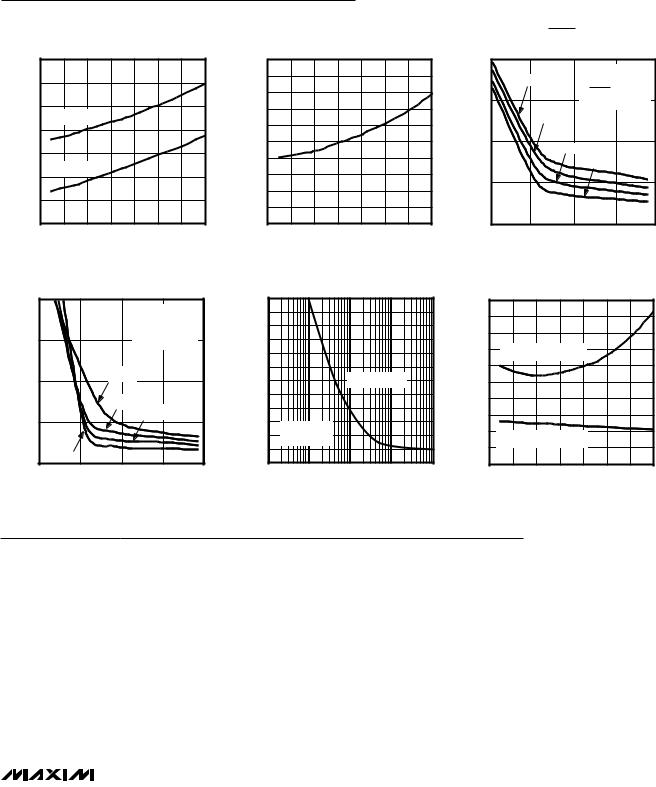
Typical Operating Characteristics
(Reset not asserted, TA = +25°C, unless otherwise noted.)
SUPPLY CURRENT vs. TEMPERATURE |
NORMALIZED RESET TIMEOUT PERIOD |
RESET (VOL) |
vs. TEMPERATURE |
vs. SUPPLY VOLTAGE |
|
6.5 |
|
|
|
|
|
|
toc01 |
|
1.050 |
|
|
|
|
|
|
|
|
|
|
|
|
6.0 |
|
|
|
|
|
|
MAX6800/01/02 |
TIMEOUT PERIOD |
1.040 |
|
|
|
|
|
|
|
1.030 |
|||
|
|
|
|
|
|
|
|
|||
|
5.5 |
VCC = +5.0V |
|
|
|
|
1.020 |
|||
|
|
|
|
|
|
|||||
A) |
|
|
|
|
|
1.010 |
||||
5.0 |
|
|
|
|
|
|
||||
|
|
|
|
|
|
|
||||
|
|
|
|
|
|
|
|
|||
( |
|
|
|
|
|
|
|
|
RESET |
1.000 |
CC |
4.5 |
|
|
|
|
|
|
|
||
|
|
|
|
|
|
|
|
|||
I |
|
|
|
|
|
|
|
0.990 |
||
|
|
|
|
|
|
|
|
NORMALIZED |
||
|
|
VCC = +3.3V |
|
|
|
|
|
|||
|
4.0 |
|
|
|
|
|
0.980 |
|||
|
|
|
|
|
|
|
|
|||
|
3.5 |
|
|
|
|
|
|
|
0.970 |
|
|
|
|
|
|
|
|
|
0.960 |
||
|
|
|
|
|
|
|
|
|
|
|
|
3.0 |
|
|
|
|
|
|
|
|
0.950 |
|
-50 |
-25 |
0 |
25 |
50 |
75 |
100 |
125 |
|
|
|
|
|
|
|
|
|
MAX6800/01/02 toc02 |
|
80 |
|
|
|
|
|
|
|
(mV) |
60 |
|
|
|
|
|
|
|
|
|
LOW |
|
|
|
|
|
|
|
|
|
OUTPUT VOLTAGE |
40 |
|
|
|
|
|
|
|
|
20 |
|
-50 |
-25 |
0 |
25 |
50 |
75 |
100 |
125 |
|
0 |
|
|
|
|
|
VTH = 2.93V |
toc03 |
|
+125°C |
MAX6800/01/02 |
||
|
ISINK = 500 A |
|||
|
|
|
RESET ASSERTED |
|
|
|
|
MAX6801/MAX6802 |
|
|
|
|
|
|
|
|
+85°C |
|
|
|
|
+25°C |
|
|
|
|
|
-40°C |
|
1.0 |
1.5 |
2.0 |
2.5 |
3.0 |
TEMPERATURE (°C) |
TEMPERATURE (°C) |
VCC (V) |
RESET (VOH) |
MAXIMUM TRANSIENT DURATION |
vs. SUPPLY VOLTAGE |
vs. RESET COMPARATOR OVERDRIVE |
(mV)) |
100 |
|
|
ISOURCE = 100 A |
toc04 |
|
600 |
|
|
|
toc05 |
|
|
|
|
500 |
|
|
|
||||
|
|
|
|
VTH = 2.93V |
MAX6800/01/02 |
DURATION(s) |
|
|
|
|
MAX6800/01/02 |
(V |
|
|
|
RESET ASSERTED |
|
|
|
|
|||
OH |
75 |
|
|
|
|
|
|
|
|
|
|
V- |
|
|
(MAX6800) |
|
|
400 |
|
|
|
|
|
CC |
|
|
|
|
|
TRANSIENTMAXIMUM |
|
|
|
|
|
HIGHVOLTAGEOUTPUT |
50 |
|
+125°C |
|
|
300 |
|
RESET OCCURS |
|
||
|
|
|
|
|
|
|
|||||
|
|
|
|
|
|
|
|
||||
|
|
|
+85°C |
|
|
200 |
|
|
|
|
|
|
|
|
|
+25°C |
|
|
|
|
|
|
|
|
25 |
|
|
|
|
|
|
|
|
|
|
|
|
|
|
|
|
|
RESET DOES |
|
|
|
|
|
|
|
|
|
|
|
100 |
|
|
|
|
|
|
|
|
|
|
|
NOT OCCUR |
|
|
|
|
|
|
|
|
|
|
|
|
|
|
|
|
|
0 |
-40°C |
|
|
|
|
0 |
|
|
|
|
|
|
|
|
|
|
|
|
|
|
||
|
1.0 |
1.5 |
2.0 |
2.5 |
3.0 |
|
0.1 |
1 |
10 |
100 |
1000 |
|
|
|
VCC (V) |
|
|
|
|
RESET COMPARATOR OVERDRIVE (mV) |
|
||
VCC FALLING PROPAGATION DELAY
vs. TEMPERATURE
|
100 |
|
|
|
|
|
|
toc06 |
|
90 |
|
|
|
|
|
|
|
|
|
|
|
|
|
|
MAX6800/01/02 |
|
( s) |
80 |
|
|
|
|
|
|
|
70 |
VCC = FALLING AT 1V/ms |
|
|
|||||
DELAY |
|
|
|
|||||
60 |
|
|
|
|
|
|
|
|
PROPAGATION |
50 |
|
|
|
|
|
|
|
40 |
|
|
|
|
|
|
|
|
30 |
|
|
|
|
|
|
|
|
20 |
|
|
|
|
|
|
|
|
|
VCC = FALLING AT 10V/ms |
|
|
|
||||
|
10 |
|
|
|
||||
|
|
|
|
|
|
|
|
|
|
0 |
|
|
|
|
|
|
|
|
-50 |
-25 |
0 |
25 |
50 |
75 |
100 |
125 |
|
|
|
|
TEMPERATURE (°C) |
|
|
||
Pin Description
|
PIN |
|
|
|
|
|
|
NAME |
FUNCTION |
MAX6800 |
|
MAX6801/ |
||
|
|
|
||
|
MAX6802 |
|
|
|
|
|
|
|
|
1 |
|
1 |
GND |
Ground |
|
|
|
|
|
|
|
|
|
Active-Low Reset Output. RESET is asserted while VCC is below the reset |
— |
|
2 |
RESET |
threshold and remains asserted for a reset timeout period (tRP) after VCC |
|
rises above the reset threshold. RESET on the MAX6801 is push/pull. |
|||
|
|
|
|
|
|
|
|
|
RESET on the MAX6802 is open-drain. |
|
|
|
|
|
|
|
|
|
Active-High Reset Output. RESET is asserted while VCC is below the reset |
2 |
|
— |
RESET |
threshold and remains asserted for a reset timeout period (tRP) after VCC |
|
|
|
|
rises above the reset threshold. RESET on the MAX6800 is push/pull. |
|
|
|
|
|
3 |
|
3 |
VCC |
Supply Voltage Input |
|
|
|
|
|
MAX6800/MAX6801/MAX6802
_______________________________________________________________________________________ 3
MAX6800/MAX6801/MAX6802
3-Pin, Low-Power
µP Reset Circuits
Applications Information
Interfacing to µPs with Bidirectional
Reset Pins
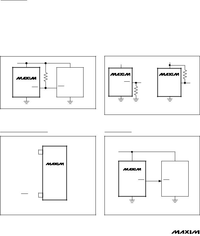
Since the RESET output on the MAX6802 is open-drain, this device interfaces easily with µPs that have bidirectional reset pins, such as the Motorola 68HC11. Connecting the µP supervisor’s RESET output directly to the microcontroller’s (µC’s) RESET pin with a single pullup resistor allows either device to assert reset (Figure 1).
VCC
VCC |
VCC |
|
100kΩ |
µP |
|
MAX6802 |
MOTOROLA |
|
68HCXX |
||
|
||
RESET |
RESET |
|
|
||
GND |
GND |
Figure 1. Interfacing to µPs with Bidirectional Reset Pins
Pin Configuration
TOP VIEW
GND 1
|
|
|
|
|
|
|
MAX6800 |
|
|
||||
MAX6801 |
|
VCC |
||||
3 |
||||||
MAX6802 |
||||||
|
|
|||||
RESET (RESET) 2
SOT23-3
( ) ARE FOR MAX6800
Negative-Going VCC Transients
In addition to issuing a reset to the µP during power-up, power-down, and brownout conditions, these devices are relatively immune to short-duration, negative-going VCC transients (glitches). The Typical Operating Characteristics show the Maximum Transient Duration vs. Reset Comparator Overdrive graph. The graph shows the maximum pulse width that a negative-going VCC transient may typically have without issuing a reset signal. As the amplitude of the transient increases, the maximum allowable pulse width decreases.
VCC VCC
MAX6801 |
100kΩ* |
MAX6800 |
|
RESET |
RESET |
GND |
100kΩ |
GND |
|
(a) |
(b) |
*ASSUMES HIGH-Z RESET INPUT TO THE µP |
|
Figure 2. Ensuring Reset Valid Down to VCC = 0
Typical Operating Circuit
VCC
VCC |
VCC |
MAX6801 |
µP |
RESET |
RESET |
GND |
GND |
4 _______________________________________________________________________________________

Ensuring a Valid Reset Output
Down to VCC = 0
When VCC falls below 1V and approaches the minimum operating voltage of 0.7V, push/pull-structured reset sinking (or sourcing) capabilities decrease drastically. High-impedance CMOS-logic inputs connected to the RESET pin can drift to indeterminate voltages. This does not present a problem in most cases, since most µPs and circuitry do not operate when VCC drops below 1V. For the MAX6801 application, where RESET must be valid down to 0, adding a pulldown resistor between RESET and GND removes stray leakage currents, holding RESET low (Figure 2a). The pulldown resistor value is not critical; 100kΩ is large enough not
3-Pin, Low-Power
µP Reset Circuits
to load RESET and small enough to pull it low. For the MAX6800 application, where RESET must be valid to VCC = 0, a 100kΩ pullup resistor between RESET and VCC will hold RESET high when VCC falls below 0.7V (Figure 2b).
Since the MAX6802 has an open-drain, active-low output, it typically uses a pullup resistor. With this device, RESET will most likely not maintain an active condition, but will drift to a non-active level due to the pullup resistor and the reduced sinking capability of the opendrain device. Therefore, this device is not recommended for applications where the RESET pin is required to be valid down to VCC = 0.
Table 1. Factory-Trimmed Reset Thresholds
RESET |
|
TA = +25°C |
|
TA = -40°C to +125°C |
||
THRESHOLD |
|
|
||||
|
|
|
|
|
||
SUFFIX |
|
|
|
|
|
|
MIN |
TYP (VTH) |
MAX |
MIN |
MAX |
||
|
||||||
48 |
4.714 |
4.80 |
4.886 |
4.656 |
4.944 |
|
47 |
4.615 |
4.70 |
4.785 |
4.559 |
4.841 |
|
|
|
|
|
|
|
|
46 |
4.547 |
4.63 |
4.713 |
4.491 |
4.769 |
|
|
|
|
|
|
|
|
45 |
4.419 |
4.50 |
4.581 |
4.365 |
4.635 |
|
|
|
|
|
|
|
|
44 |
4.301 |
4.38 |
4.459 |
4.249 |
4.511 |
|
|
|
|
|
|
|
|
43 |
4.223 |
4.30 |
4.377 |
4.171 |
4.429 |
|
|
|
|
|
|
|
|
42 |
4.124 |
4.20 |
4.276 |
4.074 |
4.326 |
|
41 |
4.026 |
4.10 |
4.174 |
3.977 |
4.223 |
|
|
|
|
|
|
|
|
40 |
3.928 |
4.00 |
4.072 |
3.880 |
4.120 |
|
|
|
|
|
|
|
|
39 |
4.830 |
3.90 |
3.970 |
3.783 |
4.017 |
|
|
|
|
|
|
|
|
38 |
3.732 |
3.80 |
3.868 |
3.686 |
3.914 |
|
|
|
|
|
|
|
|
37 |
3.633 |
3.70 |
3.767 |
3.589 |
3.811 |
|
|
|
|
|
|
|
|
36 |
3.535 |
3.60 |
3.665 |
3.492 |
3.708 |
|
|
|
|
|
|
|
|
35 |
3.437 |
3.50 |
3.563 |
3.395 |
3.605 |
|
34 |
3.339 |
3.40 |
3.461 |
3.298 |
3.502 |
|
|
|
|
|
|
|
|
33 |
3.241 |
3.30 |
3.359 |
3.201 |
3.399 |
|
|
|
|
|
|
|
|
32 |
3.142 |
3.20 |
3.258 |
3.104 |
3.296 |
|
|
|
|
|
|
|
|
31 |
3.025 |
3.08 |
3.135 |
2.988 |
3.172 |
|
|
|
|
|
|
|
|
30 |
2.946 |
3.00 |
3.054 |
2.910 |
3.090 |
|
|
|
|
|
|
|
|
29 |
2.877 |
2.93 |
2.983 |
2.842 |
3.018 |
|
28 |
2.750 |
2.80 |
2.850 |
2.716 |
2.884 |
|
|
|
|
|
|
|
|
27 |
2.651 |
2.70 |
2.749 |
2.619 |
2.781 |
|
|
|
|
|
|
|
|
26 |
2.583 |
2.63 |
2.677 |
2.551 |
2.709 |
|
|
|
|
|
|
|
|
MAX6800/MAX6801/MAX6802
_______________________________________________________________________________________ 5

MAX6800/MAX6801/MAX6802
3-Pin, Low-Power
µP Reset Circuits
Selector Guide (Standard Versions*)
PART |
OUTPUT STAGE |
NOMINAL VTH (V) |
MIN RESET |
SOT |
|
TIMEOUT (ms) |
TOP MARK |
||||
|
|
|
|||
|
|
|
|
|
|
MAX6800UR26D3-T |
Push/Pull RESET |
2.63 |
100 |
FZIE |
|
|
|
|
|
|
|
MAX6800UR29D3-T |
Push/Pull RESET |
2.93 |
100 |
FZIF |
|
|
|
|
|
|
|
MAX6800UR31D3-T |
Push/Pull RESET |
3.08 |
100 |
FZIG |
|
|
|
|
|
|
|
MAX6800UR44D3-T |
Push/Pull RESET |
4.38 |
100 |
FZIH |
|
|
|
|
|
|
|
MAX6800UR46D3-T |
Push/Pull RESET |
4.63 |
100 |
FZII |
|
|
|
|
|
|
|
MAX6801UR26D3-T |
Push/Pull RESET |
2.63 |
100 |
FZIK |
|
MAX6801UR29D3-T |
Push/Pull RESET |
2.93 |
100 |
FZIM |
|
|
|
|
|
|
|
MAX6801UR31D3-T |
Push/Pull RESET |
3.08 |
100 |
FZIN |
|
|
|
|
|
|
|
MAX6801UR44D3-T |
Push/Pull RESET |
4.38 |
100 |
FZIO |
|
|
|
|
|
|
|
MAX6801UR46D3-T |
Push/Pull RESET |
4.63 |
100 |
FZIP |
|
|
|
|
|
|
|
MAX6802UR26D3-T |
Open-Drain RESET |
2.63 |
100 |
FZIQ |
|
MAX6802UR29D3-T |
Open-Drain RESET |
2.93 |
100 |
FZIR |
|
|
|
|
|
|
|
MAX6802UR31D3-T |
Open-Drain RESET |
3.08 |
100 |
FZIS |
|
MAX6802UR44D3-T |
Open-Drain RESET |
4.38 |
100 |
FZIT |
|
|
|
|
|
|
|
MAX6802UR46D3-T |
Open-Drain RESET |
4.63 |
100 |
FZIU |
|
|
|
|
|
|
*Sample stock is generally held on all standard versions.
Chip Information
TRANSISTOR COUNT: 505
PROCESS: BiCMOS
6 _______________________________________________________________________________________
3-Pin, Low-Power
µP Reset Circuits
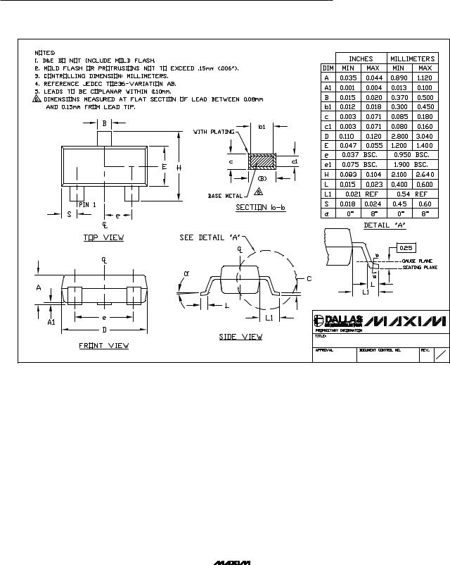
Package Information
(The package drawing(s) in this data sheet may not reflect the most current specifications. For the latest package outline information, go to www.maxim-ic.com/packages.)
|
|
|
SOT23 L.EPS |
PACKAGE OUTLINE, 3L SOT-23 |
|
|
|
21-0051 |
F |
1 |
1 |
MAX6800/MAX6801/MAX6802
Maxim cannot assume responsibility for use of any circuitry other than circuitry entirely embodied in a Maxim product. No circuit patent licenses are implied. Maxim reserves the right to change the circuitry and specifications without notice at any time.
7 _____________________Maxim Integrated Products, 120 San Gabriel Drive, Sunnyvale, CA 94086 408-737-7600
© 2005 Maxim Integrated Products |
Printed USA |
is a registered trademark of Maxim Integrated Products, Inc. |