

- •Release History
- •Contents
- •List of Figures
- •List of Tables
- •1 TMS320TCI6616 Features
- •1.1 KeyStone Architecture
- •1.2 Device Description
- •1.3 Functional Block Diagram
- •2 Device Overview
- •2.1 Device Characteristics
- •2.2 CPU (DSP Core) Description
- •2.3 Memory Map Summary
- •2.4 Boot Sequence
- •2.5 Boot Modes Supported and PLL Settings
- •2.5.1 Boot Device Field
- •2.5.2 Device Configuration Field
- •2.5.2.1 No Boot Device Configuration
- •2.5.2.2 Serial Rapid I/O Boot Device Configuration
- •2.5.2.3 Ethernet (SGMII) Boot Device Configuration
- •2.5.2.4 PCI Boot Device Configuration
- •2.5.2.5 I2C Boot Device Configuration
- •2.5.2.6 SPI Boot Device Configuration
- •2.5.2.7 HyperLink Boot Device Configuration
- •2.5.3 PLL Settings
- •2.6 Second-Level Bootloaders
- •2.7 Terminals
- •2.8 Terminal Functions
- •2.9 Development
- •2.9.1 Development Support
- •2.9.2 Device Support
- •Related Documentation from Texas Instruments
- •3 Device Configuration
- •3.1 Device Configuration at Device Reset
- •3.2 Peripheral Selection After Device Reset
- •3.3 Device State Control Registers
- •3.3.1 Device Status (DEVSTAT) Register
- •3.3.2 Device Configuration Register
- •3.3.3 JTAG ID (JTAGID) Register Description
- •3.3.4 Kicker Mechanism (KICK0 and KICK1) Register
- •3.3.5 LRESETNMI PIN Status (LRSTNMIPINSTAT) Register
- •3.3.6 LRESETNMI PIN Status Clear (LRSTNMIPINSTAT_CLR) Register
- •3.3.7 Reset Status (RESET_STAT) Register
- •3.3.8 Reset Status Clear (RESET_STAT_CLR) Register
- •3.3.9 Boot Complete (BOOTCOMPLETE) Register
- •3.3.10 Power State Control (PWRSTATECTL) Register
- •3.3.11 NMI Even Generation to CorePac (NMIGRx) Register
- •3.3.12 IPC Generation (IPCGRx) Registers
- •3.3.13 IPC Acknowledgement (IPCARx) Registers
- •3.3.14 IPC Generation Host (IPCGRH) Register
- •3.3.15 IPC Acknowledgement Host (IPCARH) Register
- •3.3.16 Timer Input Selection Register (TINPSEL)
- •3.3.17 Timer Output Selection Register (TOUTPSEL)
- •3.3.18 Reset Mux (RSTMUXx) Register
- •3.4 Pullup/Pulldown Resistors
- •4 System Interconnect
- •4.1 Internal Buses, Bridges, and Switch Fabrics
- •4.2 Data Switch Fabric Connections
- •4.3 Configuration Switch Fabric
- •4.4 Bus Priorities
- •5 C66x CorePac
- •5.1 Memory Architecture
- •5.1.1 L1P Memory
- •5.1.2 L1D Memory
- •5.1.3 L2 Memory
- •5.1.4 MSM SRAM
- •5.1.5 L3 Memory
- •5.2 Memory Protection
- •5.3 Bandwidth Management
- •5.4 Power-Down Control
- •5.5 CorePac Resets
- •5.6 CorePac Revision
- •5.7 C66x CorePac Register Descriptions
- •6 Device Operating Conditions
- •6.1 Absolute Maximum Ratings
- •6.2 Recommended Operating Conditions
- •6.3 Electrical Characteristics
- •7 TMS320TCI6616 Peripheral Information and Electrical Specifications
- •7.1 Parameter Information
- •7.1.1 1.8-V Signal Transition Levels
- •7.1.2 Timing Parameters and Board Routing Analysis
- •7.2 Recommended Clock and Control Signal Transition Behavior
- •7.3 Power Supplies
- •7.3.1 Power-Up Sequencing
- •7.3.1.1 Core-Before-IO Power Sequencing
- •7.3.1.2 IO-Before-Core Power Sequencing
- •7.3.1.3 Prolonged Resets
- •7.3.2 Power-Down Sequence
- •7.3.3 Power Supply Decoupling and Bulk Capacitors
- •7.3.4 SmartReflex
- •7.4 Enhanced Direct Memory Access (EDMA3) Controller
- •7.4.1 EDMA3 Device-Specific Information
- •7.4.2 EDMA3 Channel Synchronization Events
- •7.5 Interrupts
- •7.5.1 Interrupt Sources and Interrupt Controller
- •7.5.2 INTC Registers
- •7.5.2.1 INTC0 Register Map
- •7.5.2.2 INTC1 Register Map
- •7.5.2.3 INTC2 Register Map
- •7.5.3 Inter-Processor Register Map
- •7.5.4 NMI and LRESET
- •7.5.5 External Interrupts Electrical Data/Timing
- •7.6 Memory Protection Unit (MPU)
- •7.6.1 MPU Registers
- •7.6.1.1 MPU Register Map
- •7.6.1.2 Device-Specific MPU Registers
- •7.6.2 MPU Programmable Range Registers
- •7.6.2.1 Programmable Range n Start Address Register (PROGn_MPSAR)
- •7.6.2.2 Programmable Range n - End Address Register (PROGn_MPEAR)
- •7.6.2.3 Programmable Range n Memory Protection Page Attribute Register (PROGn_MPPA)
- •7.7 Reset Controller
- •7.7.1 Power-on Reset
- •7.7.2 Hard Reset
- •7.7.3 Soft Reset
- •7.7.4 Local Reset
- •7.7.5 Reset Priority
- •7.7.6 Reset Controller Register
- •7.7.7 Reset Electrical Data/Timing
- •7.8 Main PLL and the PLL Controller
- •7.8.1 Main PLL Controller Device-Specific Information
- •7.8.1.1 Internal Clocks and Maximum Operating Frequencies
- •7.8.1.2 Main PLL Controller Operating Modes
- •7.8.1.3 Main PLL Stabilization, Lock, and Reset Times
- •7.8.2 PLL Controller Memory Map
- •7.8.2.1 PLL Secondary Control Register (SECCTL)
- •7.8.2.2 PLL Controller Divider Register (PLLDIV2, PLLDIV5, PLLDIV8)
- •7.8.2.3 PLL Controller Clock Align Control Register (ALNCTL)
- •7.8.2.4 PLLDIV Divider Ratio Change Status Register (DCHANGE)
- •7.8.2.5 SYSCLK Status Register (SYSTAT)
- •7.8.2.6 Reset Type Status Register (RSTYPE)
- •7.8.2.7 Reset Control Register (RSTCTRL)
- •7.8.2.8 Reset Configuration Register (RSTCFG)
- •7.8.2.9 Reset Isolation Register (RSISO)
- •7.8.3 Main PLL Control Registers
- •7.8.4 Main PLL Controller/SRIO/HyperLink/PCIe Clock Input Electrical Data/Timing
- •7.9.1 DDR3 PLL Control Register
- •7.9.2 DDR3 PLL Device-Specific Information
- •7.9.3 DDR3 PLL Input Clock Electrical Data/Timing
- •7.10 PASS PLL
- •7.10.1 PASS PLL Control Register
- •7.10.2 PASS PLL Device-Specific Information
- •7.10.3 PASS PLL Input Clock Electrical Data/Timing
- •7.11 DDR3 Memory Controller
- •7.11.1 DDR3 Memory Controller Device-Specific Information
- •7.11.2 DDR3 Memory Controller Electrical Data/Timing
- •7.12 I2C Peripheral
- •7.12.1 I2C Device-Specific Information
- •7.12.2 I2C Peripheral Register Description(s)
- •7.12.3 I2C Electrical Data/Timing
- •7.12.3.1 Inter-Integrated Circuits (I2C) Timing
- •7.13 SPI Peripheral
- •7.13.1 SPI Electrical Data/Timing
- •7.13.1.1 SPI Timing
- •7.14 HyperLink Peripheral
- •7.15 UART Peripheral
- •7.16 PCIe Peripheral
- •7.17 Packet Accelerator
- •7.18 Security Accelerator
- •7.19 Ethernet MAC (EMAC)
- •7.20 Management Data Input/Output (MDIO)
- •7.21 Timers
- •7.21.1 Timers Device-Specific Information
- •7.21.2 Timers Electrical Data/Timing
- •7.22 Rake Search Accelerator (RSA)
- •7.23 Enhanced Viterbi-Decoder Coprocessor (VCP2)
- •7.24 Third-Generation Turbo Decoder Coprocessor (TCP3d)
- •7.25 Turbo Encoder Coprocessor (TCP3e)
- •7.26 Serial RapidIO (SRIO) Port
- •7.27 General-Purpose Input/Output (GPIO)
- •7.27.1 GPIO Device-Specific Information
- •7.27.2 GPIO Electrical Data/Timing
- •7.28 Semaphore2
- •7.29 Antenna Interface Subsystem 2
- •7.32 FFTC
- •7.33 Emulation Features and Capability
- •7.33.1 Advanced Event Triggering (AET)
- •7.33.2 Trace
- •7.33.2.1 Trace Electrical Data/Timing
- •7.33.3 IEEE 1149.1 JTAG
- •7.33.3.1 IEEE 1149.1 JTAG Compatibility Statement
- •7.33.3.2 JTAG Electrical Data/Timing
- •8 Mechanical Data
- •8.1 Packaging Information
- •8.2 Package CYP

TMS320TCI6616
Communications Infrastructure KeyStone SoC
www.ti.com |
SPRS624A—January 2011 |
|
7.18 Security Accelerator
The security accelerator provides wire-speed processing on 1-Gbps Ethernet traffic on IPSec, SRTP, and 3GPP Air interface security protocols. It functions on the packet level with the packet and the associated security context being one of these above three types. The security accelerator is coupled with packet accelerator, and receives the packet descriptor containing the security context in the buffer descriptor, and the data to be encrypted/decrypted in the linked buffer descriptor.
7.19 Ethernet MAC (EMAC)
The Ethernet media access controller (EMAC) modules provide an efficient interface between the TMS320TCI6616 DSP and the networked community. The EMAC supports 10Base-T (10 Mbits/second [Mbps]), and 100BaseTX (100 Mbps), in halfor full-duplex mode, and 1000BaseT (1000 Mbps) in full-duplex mode, with hardware flow control and quality-of-service (QOS) support. For more information, see the Ethernet Media Access Control (EMAC) for KeyStone Devices User Guide in ‘‘Related Documentation from Texas Instruments’’ on page 59.
Each device has a unique MAC address. There are two registers to hold these values, MACID1 (0x02620110) and MACID2 (0x02600114). All bits of these registers are defined as follows:
Figure 7-51 MACID1 Register
31 |
0 |
MACID[31:0]
R,+xxxx xxxx xxxx xxxx xxxx xxxx xxxx xxxx
Legend: R = Read only; -x, value is indeterminate
Table 7-73 |
MACID1 Register Field Descriptions |
|
|
|
|
|
||||
|
|
|
|
|
|
|
|
|
|
|
|
Bit |
Field |
Description |
|
|
|
|
|
|
|
|
31-0 |
MAC ID[31-0] |
MAC ID. A range will be assigned to this device. Each device will consume only one MAC address. |
|||||||
|
|
|
|
|
|
|
|
|
|
|
|
End of Table 7-73 |
|
|
|
|
|
|
|
|
|
|
|
|
|
|
|
|
|
|
|
|
Figure 7-52 |
MACID2 Register |
|
|
|
|
|
|
|||
31 |
|
24 |
|
23 |
18 |
17 |
16 |
15 |
0 |
|
|
|
|
|
|
|
|
|
|
|
|
|
|
CRC |
|
|
Reserved |
|
FLOW |
BCAST |
|
MACID[47:32] |
|
|
|
|
|
|
|
|
|
|
|
|
|
R+,cccc cccc |
|
|
R,+rr rrrr |
|
R,+z |
R,+y |
|
R,+xxxx xxxx xxxx xxxx |
|
Legend: R = Read only; -x, value is indeterminate |
|
|
|
|
|
|
|||
Table 7-74 |
MACID2 Register Field Descriptions |
|
|
|
|
|
||||
|
|
|
|
|
|
|
|
|
|
|
|
Bit |
Field |
Description |
|
|
|
|
|
|
|
|
31-24 |
Reserved |
Variable |
|
|
|
|
|
|
|
|
|
|
|
|
|
|
|
|
|
|
|
23-18 |
Reserved |
000000 |
|
|
|
|
|
|
|
|
|
|
|
|
|
|
|
|
|
|
|
17 |
FLOW |
MAC Flow Control |
|
|
|
|
|
|
|
|
|
|
0 = Off |
|
|
|
|
|
|
|
|
|
|
1 = On |
|
|
|
|
|
|
|
|
|
|
|
|
|
|
|
|
||
|
16 |
BCAST |
Default m/b-cast reception |
|
|
|
|
|
||
|
|
|
0 = Broadcast |
|
|
|
|
|
|
|
|
|
|
1 = Disabled |
|
|
|
|
|
|
|
|
|
|
|
|||||||
|
15-0 |
MAC ID[47-0] |
MAC ID. A range will be assigned to this device. Each device will consume only one MAC address. |
|||||||
|
|
|
|
|
|
|
|
|
|
|
|
End of Table 7-74 |
|
|
|
|
|
|
|
|
|
|
|
|
|
|
|
|
|
|
|
|
|
|
|
|
|
|
|
|
|
|
|
Copyright 2011 Texas Instruments Incorporated |
|
|
|
|
|
185 |
||||
ADVANCE INFORMATION
INFORMATION ADVANCE
TMS320TCI6616
Communications Infrastructure KeyStone SoC
SPRS624A—January 2011 |
www.ti.com |
|
7.20 Management Data Input/Output (MDIO)
The management data input/output (MDIO) module implements the 802.3 serial management interface to interrogate and controls up to 32 Ethernet PHY(s) connected to the device, using a shared two-wire bus. Application software uses the MDIO module to configure the auto-negotiation parameters of each PHY attached to the EMAC, retrieve the negotiation results, and configure required parameters in the EMAC module for correct operation. The module is designed to allow almost transparent operation of the MDIO interface, with very little maintenance from the core processor. For more information, see the Ethernet Media Access Control (EMAC) for KeyStone Devices User Guide in ‘‘Related Documentation from Texas Instruments’’ on page 59.
Table 7-75 MDIO Timing Requirements
(see Figure 7-53)
No. |
|
|
Min |
Max |
Unit |
1 |
tc(MDCLK) |
Cycle time, MDCLK |
400 |
|
ns |
|
|
|
|
|
|
|
tw(MDCLKH) |
Pulse duration, MDCLK high |
180 |
|
ns |
|
|
|
|
|
|
|
tw(MDCLKL) |
Pulse duration, MDCLK low |
180 |
|
ns |
|
|
|
|
|
|
4 |
tsu(MDIO-MDCLKH) |
Setup time, MDIO data input valid before MDCLK high |
10 |
|
ns |
|
|
|
|
|
|
5 |
th(MDCLKH-MDIO) |
Hold time, MDIO data input valid after MDCLK high |
10 |
|
ns |
|
|
|
|
|
|
|
tt(MDCLK) |
Transition time, MDCLK |
|
5 |
ns |
|
|
|
|
|
|
End of Table 7-75
Figure 7-53 |
MDIO Input Timing |
|
|
|
|
|
|
|
||||||||||
|
1 |
|
|
|
|
|
|
|
|
|
|
|
|
|||||
|
|
|
|
|
|
|
|
|
|
|
|
|
|
|
|
|||
|
|
|
|
|
|
|
|
|
|
|
|
|
|
|
|
|
|
|
|
MDCLK |
|
|
|
|
|
|
|
||||||||||
|
|
|
|
|
|
|
|
|
|
|
|
|
|
|
|
|
|
|
|
4 |
|
5 |
|
|
|
|
|
||||||||||
|
|
|
|
|
|
|
|
|
|
|
|
|
||||||
|
|
|
|
|
|
|
|
|
|
|
|
|
|
|
|
|
|
|
|
MDIO |
|
|
|
|
|
|
|
||||||||||
|
(Input) |
|
|
|
|
|
|
|
|
|
|
|||||||
Table 7-76 |
MDIO Switching Characteristics |
|
|
|
|
(see Figure 7-54) |
|
|
|
|
|
|
|
|
|
|
|
No. |
|
Parameter |
Min |
Max |
Unit |
7 |
td(MDCLKL-MDIO) |
Delay time, MDCLK low to MDIO data output valid |
|
100 |
ns |
|
|
|
|
|
|
End of Table 7-76 |
|
|
|
|
|
|
|
|
|
|
|
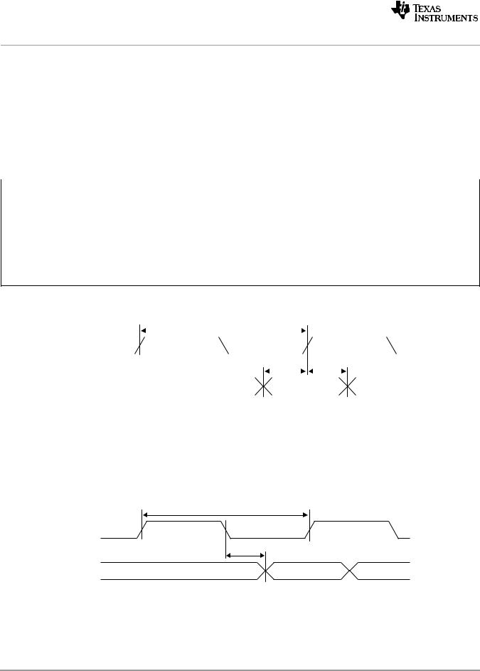
Figure 7-54 MDIO Output Timing
1
MDCLK
7
MDIO (Ouput)
186 |
Copyright 2011 Texas Instruments Incorporated |