

- •Release History
- •Contents
- •List of Figures
- •List of Tables
- •1 TMS320TCI6616 Features
- •1.1 KeyStone Architecture
- •1.2 Device Description
- •1.3 Functional Block Diagram
- •2 Device Overview
- •2.1 Device Characteristics
- •2.2 CPU (DSP Core) Description
- •2.3 Memory Map Summary
- •2.4 Boot Sequence
- •2.5 Boot Modes Supported and PLL Settings
- •2.5.1 Boot Device Field
- •2.5.2 Device Configuration Field
- •2.5.2.1 No Boot Device Configuration
- •2.5.2.2 Serial Rapid I/O Boot Device Configuration
- •2.5.2.3 Ethernet (SGMII) Boot Device Configuration
- •2.5.2.4 PCI Boot Device Configuration
- •2.5.2.5 I2C Boot Device Configuration
- •2.5.2.6 SPI Boot Device Configuration
- •2.5.2.7 HyperLink Boot Device Configuration
- •2.5.3 PLL Settings
- •2.6 Second-Level Bootloaders
- •2.7 Terminals
- •2.8 Terminal Functions
- •2.9 Development
- •2.9.1 Development Support
- •2.9.2 Device Support
- •Related Documentation from Texas Instruments
- •3 Device Configuration
- •3.1 Device Configuration at Device Reset
- •3.2 Peripheral Selection After Device Reset
- •3.3 Device State Control Registers
- •3.3.1 Device Status (DEVSTAT) Register
- •3.3.2 Device Configuration Register
- •3.3.3 JTAG ID (JTAGID) Register Description
- •3.3.4 Kicker Mechanism (KICK0 and KICK1) Register
- •3.3.5 LRESETNMI PIN Status (LRSTNMIPINSTAT) Register
- •3.3.6 LRESETNMI PIN Status Clear (LRSTNMIPINSTAT_CLR) Register
- •3.3.7 Reset Status (RESET_STAT) Register
- •3.3.8 Reset Status Clear (RESET_STAT_CLR) Register
- •3.3.9 Boot Complete (BOOTCOMPLETE) Register
- •3.3.10 Power State Control (PWRSTATECTL) Register
- •3.3.11 NMI Even Generation to CorePac (NMIGRx) Register
- •3.3.12 IPC Generation (IPCGRx) Registers
- •3.3.13 IPC Acknowledgement (IPCARx) Registers
- •3.3.14 IPC Generation Host (IPCGRH) Register
- •3.3.15 IPC Acknowledgement Host (IPCARH) Register
- •3.3.16 Timer Input Selection Register (TINPSEL)
- •3.3.17 Timer Output Selection Register (TOUTPSEL)
- •3.3.18 Reset Mux (RSTMUXx) Register
- •3.4 Pullup/Pulldown Resistors
- •4 System Interconnect
- •4.1 Internal Buses, Bridges, and Switch Fabrics
- •4.2 Data Switch Fabric Connections
- •4.3 Configuration Switch Fabric
- •4.4 Bus Priorities
- •5 C66x CorePac
- •5.1 Memory Architecture
- •5.1.1 L1P Memory
- •5.1.2 L1D Memory
- •5.1.3 L2 Memory
- •5.1.4 MSM SRAM
- •5.1.5 L3 Memory
- •5.2 Memory Protection
- •5.3 Bandwidth Management
- •5.4 Power-Down Control
- •5.5 CorePac Resets
- •5.6 CorePac Revision
- •5.7 C66x CorePac Register Descriptions
- •6 Device Operating Conditions
- •6.1 Absolute Maximum Ratings
- •6.2 Recommended Operating Conditions
- •6.3 Electrical Characteristics
- •7 TMS320TCI6616 Peripheral Information and Electrical Specifications
- •7.1 Parameter Information
- •7.1.1 1.8-V Signal Transition Levels
- •7.1.2 Timing Parameters and Board Routing Analysis
- •7.2 Recommended Clock and Control Signal Transition Behavior
- •7.3 Power Supplies
- •7.3.1 Power-Up Sequencing
- •7.3.1.1 Core-Before-IO Power Sequencing
- •7.3.1.2 IO-Before-Core Power Sequencing
- •7.3.1.3 Prolonged Resets
- •7.3.2 Power-Down Sequence
- •7.3.3 Power Supply Decoupling and Bulk Capacitors
- •7.3.4 SmartReflex
- •7.4 Enhanced Direct Memory Access (EDMA3) Controller
- •7.4.1 EDMA3 Device-Specific Information
- •7.4.2 EDMA3 Channel Synchronization Events
- •7.5 Interrupts
- •7.5.1 Interrupt Sources and Interrupt Controller
- •7.5.2 INTC Registers
- •7.5.2.1 INTC0 Register Map
- •7.5.2.2 INTC1 Register Map
- •7.5.2.3 INTC2 Register Map
- •7.5.3 Inter-Processor Register Map
- •7.5.4 NMI and LRESET
- •7.5.5 External Interrupts Electrical Data/Timing
- •7.6 Memory Protection Unit (MPU)
- •7.6.1 MPU Registers
- •7.6.1.1 MPU Register Map
- •7.6.1.2 Device-Specific MPU Registers
- •7.6.2 MPU Programmable Range Registers
- •7.6.2.1 Programmable Range n Start Address Register (PROGn_MPSAR)
- •7.6.2.2 Programmable Range n - End Address Register (PROGn_MPEAR)
- •7.6.2.3 Programmable Range n Memory Protection Page Attribute Register (PROGn_MPPA)
- •7.7 Reset Controller
- •7.7.1 Power-on Reset
- •7.7.2 Hard Reset
- •7.7.3 Soft Reset
- •7.7.4 Local Reset
- •7.7.5 Reset Priority
- •7.7.6 Reset Controller Register
- •7.7.7 Reset Electrical Data/Timing
- •7.8 Main PLL and the PLL Controller
- •7.8.1 Main PLL Controller Device-Specific Information
- •7.8.1.1 Internal Clocks and Maximum Operating Frequencies
- •7.8.1.2 Main PLL Controller Operating Modes
- •7.8.1.3 Main PLL Stabilization, Lock, and Reset Times
- •7.8.2 PLL Controller Memory Map
- •7.8.2.1 PLL Secondary Control Register (SECCTL)
- •7.8.2.2 PLL Controller Divider Register (PLLDIV2, PLLDIV5, PLLDIV8)
- •7.8.2.3 PLL Controller Clock Align Control Register (ALNCTL)
- •7.8.2.4 PLLDIV Divider Ratio Change Status Register (DCHANGE)
- •7.8.2.5 SYSCLK Status Register (SYSTAT)
- •7.8.2.6 Reset Type Status Register (RSTYPE)
- •7.8.2.7 Reset Control Register (RSTCTRL)
- •7.8.2.8 Reset Configuration Register (RSTCFG)
- •7.8.2.9 Reset Isolation Register (RSISO)
- •7.8.3 Main PLL Control Registers
- •7.8.4 Main PLL Controller/SRIO/HyperLink/PCIe Clock Input Electrical Data/Timing
- •7.9.1 DDR3 PLL Control Register
- •7.9.2 DDR3 PLL Device-Specific Information
- •7.9.3 DDR3 PLL Input Clock Electrical Data/Timing
- •7.10 PASS PLL
- •7.10.1 PASS PLL Control Register
- •7.10.2 PASS PLL Device-Specific Information
- •7.10.3 PASS PLL Input Clock Electrical Data/Timing
- •7.11 DDR3 Memory Controller
- •7.11.1 DDR3 Memory Controller Device-Specific Information
- •7.11.2 DDR3 Memory Controller Electrical Data/Timing
- •7.12 I2C Peripheral
- •7.12.1 I2C Device-Specific Information
- •7.12.2 I2C Peripheral Register Description(s)
- •7.12.3 I2C Electrical Data/Timing
- •7.12.3.1 Inter-Integrated Circuits (I2C) Timing
- •7.13 SPI Peripheral
- •7.13.1 SPI Electrical Data/Timing
- •7.13.1.1 SPI Timing
- •7.14 HyperLink Peripheral
- •7.15 UART Peripheral
- •7.16 PCIe Peripheral
- •7.17 Packet Accelerator
- •7.18 Security Accelerator
- •7.19 Ethernet MAC (EMAC)
- •7.20 Management Data Input/Output (MDIO)
- •7.21 Timers
- •7.21.1 Timers Device-Specific Information
- •7.21.2 Timers Electrical Data/Timing
- •7.22 Rake Search Accelerator (RSA)
- •7.23 Enhanced Viterbi-Decoder Coprocessor (VCP2)
- •7.24 Third-Generation Turbo Decoder Coprocessor (TCP3d)
- •7.25 Turbo Encoder Coprocessor (TCP3e)
- •7.26 Serial RapidIO (SRIO) Port
- •7.27 General-Purpose Input/Output (GPIO)
- •7.27.1 GPIO Device-Specific Information
- •7.27.2 GPIO Electrical Data/Timing
- •7.28 Semaphore2
- •7.29 Antenna Interface Subsystem 2
- •7.32 FFTC
- •7.33 Emulation Features and Capability
- •7.33.1 Advanced Event Triggering (AET)
- •7.33.2 Trace
- •7.33.2.1 Trace Electrical Data/Timing
- •7.33.3 IEEE 1149.1 JTAG
- •7.33.3.1 IEEE 1149.1 JTAG Compatibility Statement
- •7.33.3.2 JTAG Electrical Data/Timing
- •8 Mechanical Data
- •8.1 Packaging Information
- •8.2 Package CYP

TMS320TCI6616
Communications Infrastructure KeyStone SoC
www.ti.com |
SPRS624A—January 2011 |
|
7.11.2 DDR3 Memory Controller Electrical Data/Timing
The DDR3 Implementation Guidelines application report in ‘‘Related Documentation from Texas Instruments’’ on page 59 specifies a complete DDR3 interface solution as well as a list of compatible DDR3 devices. The DDR3 electrical requirements are fully specified in the DDR3 Jedec Specification JESD79-3C. TI has performed the simulation and system characterization to ensure all DDR3 interface timings in this solution are met; therefore, no electrical data/timing information is supplied here for this interface.
Note—TI supports only designs that follow the board design guidelines outlined in the application report.
7.12 I2C Peripheral
The inter-integrated circuit (I2C) module provides an interface between DSP and other devices compliant with Philips Semiconductors Inter-IC bus (I2C bus) specification version 2.1 and connected by way of an I2C bus. External components attached to this 2-wire serial bus can transmit/receive up to 8-bit data to/from the DSP through the I2C module.
7.12.1 I2C Device-Specific Information
The TMS320TCI6616 device includes an I2C peripheral module. NOTE: when using the I2C module, ensure there are external pullup resistors on the SDA and SCL pins.
The I2C modules on the TCI6616 may be used by the DSP to control local peripheral ICs (DACs, ADCs, etc.) or may be used to communicate with other controllers in a system or to implement a user interface.
The I2C port supports:
•Compatible with Philips I2C specification revision 2.1 (January 2000)
•Fast mode up to 400 Kbps (no fail-safe I/O buffers)
•Noise filter to remove noise 50 ns or less
•7-bit and 10-bit device addressing modes
•Multi-master (transmit/receive) and slave (transmit/receive) functionality
•Events: DMA, interrupt, or polling
•Slew-rate limited open-drain output buffers
ADVANCE INFORMATION
Copyright 2011 Texas Instruments Incorporated |
173 |
TMS320TCI6616
Communications Infrastructure KeyStone SoC
SPRS624A—January 2011 |
www.ti.com |
|
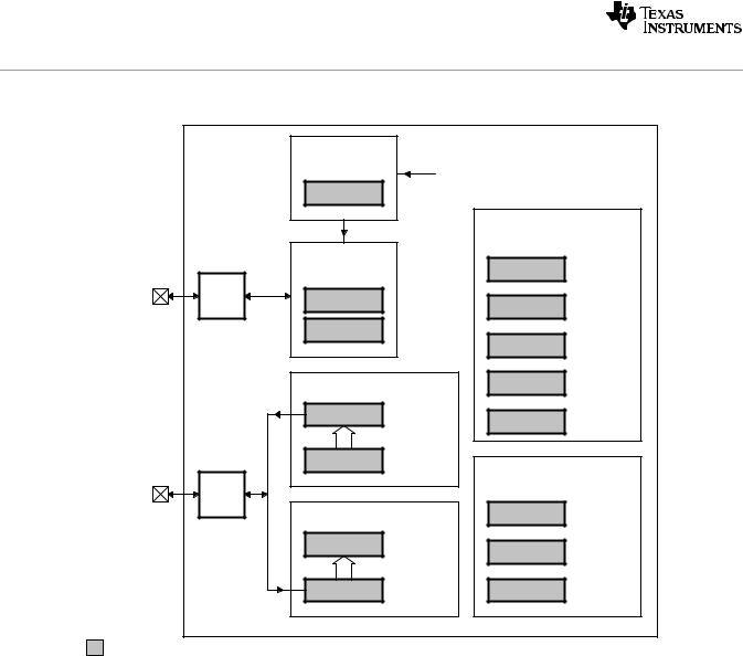
Figure 7-39 shows a block diagram of the I2C module.
Figure 7-39 I2C Module Block Diagram
INFORMATION ADVANCE
|
|
I2C Module |
|
|
|
|
|
|
|
|
|
|
|
|
|
Clock |
|
|
|
|
|
|
|
|
|
|
Prescale |
|
Peripheral Clock |
|
|||||
|
|
|
|
|
|
|
|
||||
|
|
|
I2CPSC |
|
(CPU/6) |
|
|
|
|
||
|
|
|
|
|
|
|
|
|
|||
|
|
|
|
|
|
|
Control |
|
|||
|
|
|
Bit Clock |
|
|
2 |
|
|
Own |
||
|
|
SCL |
Generator |
|
I |
COAR |
Address |
||||
|
|
|
|
|
|
|
|
|
|
|
|
2 |
|
Noise |
2 |
|
|
|
|
|
|
|
|
I C Clock |
Filter |
|
|
|
|
|
|
|
Slave |
||
I CCLKH |
|
I2CSAR |
|||||||||
|
|
|
|
|
|
|
|
|
|
|
Address |
|
|
|
I2CCLKL |
|
|
|
|
|
|
||
|
|
|
|
|
|
|
I2CMDR |
Mode |
|||
|
|
|
Transmit |
|
I2CCNT |
Data |
|||||
|
|
|
|
|
|
|
|
Count |
|||
|
|
|
I2CXSR |
Transmit |
2 |
CEMDR |
Extended |
||||
|
|
|
|
|
|
Shift |
I |
Mode |
|||
|
|
|
|
|
|
|
|
|
|
|
|
|
|
|
I2CDXR |
Transmit |
|
|
|
|
|
||
|
|
SDA |
|
|
|
Buffer |
Interrupt/DMA |
|
|||
|
|
|
|
|
|
|
|||||
|
I2C Data |
Noise |
|
|
|
|
|
|
|
|
|
|
|
Filter |
|
|
|
|
|
|
|
|
Interrupt |
|
|
|
Receive |
|
I2CIMR |
||||||
|
|
|
|
|
|
|
|
Mask/Status |
|||
|
|
|
|
2 |
|
Receive |
|
|
|
|
|
|
|
|
I |
CDRR |
Buffer |
|
2 |
CSTR |
Interrupt |
||
|
|
|
|
|
|
|
I |
|
Status |
||
|
|
|
|
|
|
|
|
|
|
|
|
|
|
|
I2CRSR |
Receive |
|
I2CIVR |
Interrupt |
||||
|
|
|
|
Vector |
|||||||
|
|
|
|
|
|
Shift |
|
|
|
|
|
Shading denotes control/status registers.
7.12.2 I2C Peripheral Register Description(s)
Table 7-64 |
I2C Registers (Part 1 of 2) |
|
|
Hex Address Range |
Acronym |
Register Name |
|
0253 0000 |
ICOAR |
I2C own address register |
|
0253 0004 |
ICIMR |
I2C interrupt mask/status register |
|
0253 0008 |
ICSTR |
I2C interrupt status register |
|
0253 000C |
ICCLKL |
I2C clock low-time divider register |
|
0253 0010 |
ICCLKH |
I2C clock high-time divider register |
|
0253 0014 |
ICCNT |
I2C data count register |
|
0253 0018 |
ICDRR |
I2C data receive register |
|
0253 001C |
ICSAR |
I2C slave address register |
|
0253 0020 |
ICDXR |
I2C data transmit register |
|
0253 0024 |
ICMDR |
I2C mode register |
|
0253 0028 |
ICIVR |
I2C interrupt vector register |
|
0253 002C |
ICEMDR |
I2C extended mode register |
|
0253 0030 |
ICPSC |
I2C prescaler register |
|
|
|
|
|
174 |
|
|
Copyright 2011 Texas Instruments Incorporated |