

Добавил:
Upload
Опубликованный материал нарушает ваши авторские права? Сообщите нам.
Вуз:
Предмет:
Файл:
TMS320TCI6616
Communications Infrastructure KeyStone SoC
www.ti.com |
SPRS624A—January 2011 |
|
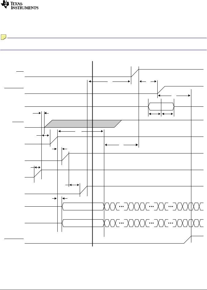
7.3.1.2 IO-Before-Core Power Sequencing
The timing diagram for IO-before-core power sequencing is shown in Figure 7-6 and defined in Table 7-4.
Note—TI recommends a maximum of 100 ms between one power rail being valid, and the next power rail in the sequence starting to ramp.
Figure 7-6 |
IO Before Core Power Sequencing |
|
|
|
|
|
|
Power Stabilization Phase |
Device Initialization Phase |
|
|
|
|
POR |
|
|
|
|
|
INFORMATION |
|
|
t5 |
t7 |
|
|
|
|
|
|
|
|
||
RESETFULL |
|
|
|
|
|
|
|
|
|
|
|
t8 |
|
GPIO Config |
|
|
|
|
|
|
Bits |
|
|
|
|
|
|
|
t2a |
|
|
|
|
|
|
|
|
t9 |
t10 |
|
|
RESET |
|
|
|
|
|
|
|
t3c |
|
|
|
|
ADVANCE |
|
t1 |
|
|
|
|
|
|
t2b |
|
|
|
|
|
CVDD |
|
|
|
|
|
|
|
|
t6 |
|
|
|
|
|
t3a |
|
|
|
|
|
CVDD1 |
|
|
|
|
|
|
DVDD18 |
|
|
|
|
|
|
|
t4 |
|
|
|
|
|
DVDD15 |
|
|
|
|
|
|
|
t3b |
|
|
|
|
|
REFCLKP&N |
|
|
|
|
|
|
DDRCLKP&N |
|
|
|
|
|
|
RESETSTAT |
|
|
|
|
|
|
Copyright 2011 Texas Instruments Incorporated |
99 |