

ADSP-21160M
With the ADSP-21160M’s separate program and data memory buses and on-chip instruction cache, the processor can simultaneously fetch four operands and an instruction (from the cache), all in a single cycle.
Instruction Cache
The ADSP-21160M includes an on-chip instruction cache that enables three-bus operation for fetching an instruction and four data values. The cache is selective—only the instructions whose fetches conflict with PM bus data accesses are cached. This cache allows full-speed execution of core, providing looped operations such as digital filter multiplyaccumulates and FFT butterfly processing.
Data Address Generators with Hardware Circular Buffers
The ADSP-21160M’s two data address generators (DAGs) are used for indirect addressing and provide for implementing circular data buffers in hardware. Circular buffers allow efficient programming of delay lines and other data structures required in digital signal processing, and are commonly used in digital filters and Fourier transforms. The two DAGs of the ADSP-21160M contain sufficient registers to allow the creation of up to 32 circular buffers (16 primary register sets, 16 secondary). The DAGs automatically handle address pointer wraparound, reducing overhead, increasing performance, and simplifying implementation. Circular buffers can start and end at any memory location.
Flexible Instruction Set
The 48-bit instruction word accommodates a variety of parallel operations, for concise programming. For example, the ADSP-21160M can conditionally execute a multiply, an add, and subtract, in both processing elements, while branching, all in a single instruction.
ADSP-21160M Memory and I/O Interface Features
Augmenting the ADSP-2116x family core, the ADSP-21160M adds the following architectural features:
Dual-Ported On-Chip Memory
The ADSP-21160M contains four megabits of on-chip SRAM, organized as two blocks of 2 Mbits each, which can be configured for different combinations of code and data storage. Each memory block is dual-ported for single-cycle, independent accesses by the core processor and I/O processor. The dual-ported memory in combination with three separate on-chip buses allows two data transfers from the core and one from I/O processor, in a single cycle. On the ADSP-21160M, the memory can be configured as a maximum of 128K words of 32-bit data, 256K words of 16-bit data, 85K words of 48-bit instructions (or 40-bit data), or combinations of different word sizes up to four megabits. All of the memory can be accessed as 16-bit, 32-bit, 48-bit, or 64-bit words. A 16-bit floating-point storage format is supported that effectively doubles the amount of data that may be stored on-chip. Conversion
between the 32-bit floating-point and 16-bit floating-point formats is done in a single instruction. While each memory block can store combinations of code and data, accesses are most efficient when one block stores data, using the DM bus for transfers, and the other block stores instructions and data, using the PM bus for transfers. Using the DM bus and PM bus in this way, with one dedicated to each memory block, assures single-cycle execution with two data transfers. In this case, the instruction must be available in
the cache.
Off-Chip Memory and Peripherals Interface
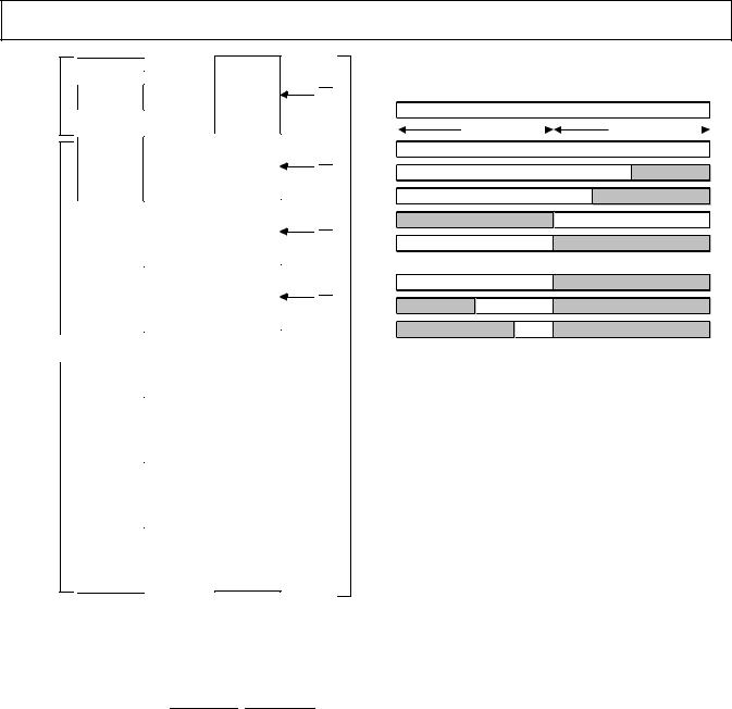
The ADSP-21160M’s external port provides the processor’s interface to off-chip memory and peripherals. The 4G word off-chip address space is included in the ADSP-21160M’s unified address space. The separate on-chip buses—for PM addresses, PM data, DM addresses, DM data, I/O addresses, and I/O data—are multiplexed at the external port to create an external system bus with a single 32-bit address bus and a single 64-bit data bus. The lower 32 bits of the external data bus connect to even addresses and the upper 32 bits of the 64 connect to odd addresses. Every access to external memory is based on an address that fetches a 32-bit word, and with the 64-bit bus, two address locations can be accessed at once. When fetching an instruction from external memory, two 32-bit data locations are being accessed (16 bits are unused). Figure 3 shows the alignment of various accesses to external memory.
The external port supports asynchronous, synchronous, and synchronous burst accesses. ZBT synchronous burst SRAM can be interfaced gluelessly. Addressing of external memory devices is facilitated by on-chip decoding of high-order address lines to generate memory bank select signals. Separate control lines are also generated for simplified addressing of page-mode DRAM. The ADSP-21160M provides programmable memory wait states and external memory acknowledge controls to allow interfacing to DRAM and peripherals with variable access, hold, and disable time requirements.
DMA Controller
The ADSP-21160M’s on-chip DMA controller allows zero-overhead data transfers without processor intervention. The DMA controller operates independently and invisibly to the processor core, allowing DMA operations to occur while the core is simultaneously executing its program instructions. DMA transfers can occur between the ADSP-21160M’s internal memory and external memory, external peripherals, or a host processor. DMAtransfers can also occur between the ADSP-21160M’s internal memory and its serial ports or link ports. External bus packing to 16-, 32-, 48-, or 64-bit words is performed during DMA transfers. Fourteen channels of DMA are available on the ADSP-21160M—six via the link ports, four via the serial ports, and four via the processor’s external port (for either
–4– |
REV. 0 |
ADSP-21160M
,QWHUQDO
0HPRU\
6SDFH
0XOWLSURFHVVRU
0HPRU\
6SDFH
,23 5HJ¶V
/RQJ :RUG
1RUPDO :RUG
6KRUW :RUG
,QWHUQDO
0HPRU\
6SDFH,'
,QWHUQDO
0HPRU\
6SDFH,'
,QWHUQDO
0HPRU\
6SDFH,'
,QWHUQDO
0HPRU\
6SDFH,'
,QWHUQDO
0HPRU\
6SDFH,'
,QWHUQDO
0HPRU\
6SDFH,'
%URDGFDVW :ULWH WR $OO '63V,'
[ |
[ |
|
[ |
|
|
[ |
06 |
|
%DQN |
||
|
||
[ |
|
|
[ |
|
|
%DQN |
06 |
|
[ |
|
|
%DQN |
06 |
|
[ |
|
|
%DQN |
06 |
|
[ |
|
|
|
([WHUQDO |
|
|
0HPRU\ |
|
|
6SDFH |
|
[ |
|
|
1RQEDQNHG |
|
|
[ |
|
|
[ |
|
|
[ ) )))) |
[)))) )))) |
Figure 2. ADSP-21160M Memory Map
host processor, other ADSP-21160Ms, memory or I/O transfers). Programs can be downloaded to the ADSP-21160M using DMA transfers. Asynchronous off-chip peripherals can control two DMA channels using DMA Request/Grant lines (DMAR1–2, DMAG1–2). Other DMA features include interrupt generation upon completion of DMA transfers, two-dimensional DMA, and DMA chaining for automatic linked DMA transfers.
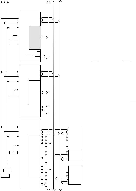
Multiprocessing
The ADSP-21160M offers powerful features tailored to multiprocessing DSP systems as shown in Figure 4. The external port and link ports provide integrated glueless multiprocessing support.
The external port supports a unified address space (see Figure 2) that allows direct interprocessor accesses of each ADSP-21160M’s internal memory. Distributed bus arbitrationlogic is includedon-chipfor simple, glueless connection of systems containing up to six ADSP-21160Ms and a host processor. Master processor changeover incurs only one cycle of overhead. Bus arbitration is selectable as either fixed
REV. 0
'$7$ ±
|
|
|
|
|
|
|
|
|
|
|||
|
%<7( |
|
|
|
|
|
|
|
|
|
%<7( |
|
|
|
|
|
|
|
|
|
|
|
|
|
|
|
|
|
|
|
|
|
|
|
|
|
|
|
|
|
5'+ :5+ |
|
|
|
|
5'/ :5/ |
|
|
|||
|
|
|
|
|
|
|
|
|
|
|
|
|
%,7 /21* :25' 6,0' '0$ ,23 5(*,67(5 75$16)(56
%,7 75$16)(5 )25 %,7 ,16758&7,21 )(7&+
%,7 75$16)(5 )25 %,7 (;7(1'(' 35(&,6,21
%,7 1250$/ :25' (9(1 $''5(66
%,7 1250$/ :25' 2'' $''5(66
5(675,&7(' '0$ +267 (3520 '$7$ $/,*10(176
%,7 3$&.('
%,7 3$&.('
(3520
Figure 3. ADSP-21160M External Data Alignment Options
or rotating priority. Bus lock allows indivisible read-mod- ify-write sequences for semaphores. A vector interrupt is provided for interprocessor commands. Maximum throughput for interprocessor data transfer is 320M bytes/s over the external port. Broadcast writes allow simultaneous transmission of data to all ADSP-21160Ms and can be used to implement reflective semaphores.
Six link ports provide for a second method of multiprocessing communications. Each link port can support communications to another ADSP-21160M. Using the links, a large multiprocessor system can be constructed in a 2D or 3D fashion. Systems can use the link ports and cluster multiprocessing concurrently or independently.
Link Ports
The ADSP-21160M features six 8-bit link ports that provide additional I/O capabilities. With the capability of running at 80 MHz rates, each link port can support 80M bytes/s. Link port I/O is especially useful for point-to-point interprocessor communication in multiprocessing systems. The link ports can operate independently and simultaneously. Link port data is packed into 48or 32-bit words, and can be directly read by the core processor or DMA-transferred to on-chip memory. Each link port has its own double-buffered input and output registers. Clock/acknowledge handshaking controls link port transfers. Transfers are programmable as either transmit
or receive. For data throughput information, see link port timing details in Table 18 on page 34.
Serial Ports
The ADSP-21160M features two synchronous serial ports that provide an inexpensive interface to a wide variety of digital and mixed-signal peripheral devices. The serial ports can operate up to half the clock rate of the core, providing each with a maximum data rate of 40M bit/s. Independent
–5–
ADSP-21160M
|
|
$'63 |
[ |
|
|
|
|
|
|
$'63 |
[ |
|
|
|
|
|
|
$'63 |
[ |
&21752/ |
$''5(66 |
|
|
|
|
|
|
'$7$ |
|||
|
|
$'63 |
[ |
||||
&/.,1 |
$'' |
5 ± |
|
|
|
||
|
|
|
|
|
|||
|
|
|
'$7 |
$ ± |
|
|
|
5 |
(6(7 |
|
|
|
|
|
|
5 |
3%$ |
|
|
|
|
|
|

 ,' ±
,' ±
&21752/
3$ 
 %5 ± %5 ±
%5
|
|
|
|
$'63 [ |
|
|
|
|
|
|
|
|
|
|
|
|
|
|
|
|
|
|||||||||||
&/.,1 |
|
|
$'' 5 ± |
|
|
|
|
|
|
|
|
|
|
|
|
|
||||||||||||||||
|
|
|
|
|
|
|
'$7$ ± |
|
|
|
|
|
|
|
|
|
|
|
|
|
||||||||||||
5(6(7 |
|
|
|
|
|
|
|
|
|
|
|
|
|
|
|
|
|
|
|
|
|
|
|
|
|
|
|
|
||||
53%$ |
|
|
|
|
|
|
|
|
|
|
|
|
|
|
|
|
|
|
|
|
|
|
|
|
|
|
|
|
||||
|
|
|
|
|
|
|
|
|
|
|
|
|
|
|
|
|
|
|
|
|
|
|
|
|
|
|
|
|||||
|
|
|
|
|
|
|
|
|
|
|
|
|
|
|
|
|
|
|
|
|
|
|
|
|
|
|
|
|
|
|||
|
|
|
|
,' ± |
|
|
|
|
|
|
|
|
|
|
|
|
|
|
|
|
|
|
|
|
|
|
|
|
|
|
|
|
|
|
|
|
|
|
|
&21752/ |
|
|
|
|
|
|
|
|
|
|
|
|
|
|
|
|
|||||||||
|
|
|
|
|
|
|
|
|
|
|
|
|
|
|
|
|
|
|
|
|
|
|
|
|
|
|
|
|
|
|||
|
|
|
|
|
|
|
|
|
|
|
|
|
|
|
|
|
|
|
|
|
|
|
|
|
|
|
|
|
|
|
||
|
|
|
|
|
|
|
|
|
|
|
|
|
|
|
|
|
|
|
|
|
|
|
|
|
|
|
|
|
|
|
|
|
|
|
|
|
|
|
|
|
|
|
|
|
|
|
|
|
|
|
|
|
|
|
|
|
|
|
|
|
|
|
|
|
|
|
|
|
|
|
|
|
|
|
|
|
|
|
|
|
|
|
|
|
|
|
|
|
|
|
|
|
|
|
||||
|
|
|
|
|
|
|
|
3 |
$ |
|
|
|
|
|
|
|
|
|
|
|
|
|
|
|
|
|||||||
|
|
|
|
|
|
|
|
|
|
|
|
|
|
|
||||||||||||||||||
|
|
|
|
|
|
%5 %5 ± |
|
|
|
|
|
|
|
|
||||||||||||||||||
|
|
|
|
|
|
|
|
|
|
|
|
|
|
|
|
|
|
|
|
|
|
|
|
|
|
|
|
|
|
|
|
|
|
|
|
|
|
|
|
|
|
|
|
|
|
%5 |
|
|
|
|
|
|
|
|
|
|
|
|
|
|
|||||
|
|
|
|
|
|
|
|
|
|
|
|
|
|
|
|
|
|
|
|
&21752/ |
$''5(66 |
'$7$ |
*/2%$/ |
|||||||||
|
|
|
|
|
|
|
|
|
|
|
|
|
|
|
|
|
|
|
|
|
|
|
23 7,21 |
$/ |
||||||||
|
|
|
|
|
|
|
|
|
|
|
|
|
|
|
|
|
|
|
|
|
|
|
|
|
|
|
0( 02 5< |
|||||
|
|
|
|
$'63 [ |
|
|
|
|
|
|
|
|
|
|
|
$1 ' |
|
|||||||||||||||
|
|
|
|
|
|
|
|
|
|
|
|
|
|
|
3( 5,3+ (5$/6 |
|||||||||||||||||
&/.,1 |
|
|
|
|
|
|
|
|
|
|
|
|
|
|
|
|
|
|
|
|
|
|
|
|
|
|
|
|
||||
|
|
$''5 ± |
|
|
|
|
|
|
|
|
$''5 |
|
||||||||||||||||||||
|
|
|
|
|
|
|
|
|
|
|
|
|
|
|
|
|||||||||||||||||
5(6(7 |
|
|
'$7$ ± |
|
|
|
|
|
|
|
|
|
|
|
|
|
||||||||||||||||
|
|
|
|
|
|
|
|
|
|
|
|
|
|
|
'$7 $ |
|
||||||||||||||||
|
|
|
|
|
|
|
|
|
|
|
|
|
|
|
|
|
|
|
|
|
|
|
|
|
|
|
|
|
||||
53%$ |
|
|
|
|
|
|
|
|
|
|
|
|
|
|
|
|
|
|
|
|
|
|
|
|
|
|
|
|
||||
|
|
|
|
5'; |
|
|
|
|
|
|
|
|
|
|
|
2( |
|
|
||||||||||||||
|
|
|
|
|
|
|
|
|
|
|
|
|
|
|
|
|
|
|
||||||||||||||
|
|
|
|
|
: 5; |
|
|
|
|
|
|
|
|
|
|
|
: ( |
|
|
|||||||||||||
|
|
|
|
|
|
|
|
|
|
|
|
|
||||||||||||||||||||
|
|
|
|
$&. |
|
|
|
|
|
|
|
|
|
|
|
$&. |
|
|||||||||||||||
|
|
|
|
|
|
|
|
|
||||||||||||||||||||||||
|
|
|
|
,' ± |
|
|
|
|
0 6 ± |
|
|
|
|
|
|
|
|
|
|
|
|
|
|
|||||||||
|
|
|
|
|
|
|
|
|
|
|
|
|
|
|
|
|
|
&6 |
|
|
||||||||||||
|
|
|
|
|
|
|
|
|
|
|
|
|
|
|
|
|
|
|
|
|
|
|
|
|
|
|
|
|
|
|||
|
|
|
|
|
|
|
|
|
|
|
|
|
|
|
|
|
|
|
|
|
|
|
|
|
|
|
|
|
|
|
||
|
|
|
|
|
%06 |
|
|
|
|
|
|
|
|
|
|
|
|
&6 |
|
|
||||||||||||
|
|
|
|
|
|
|
3$* ( |
|
|
|
|
|
|
|
|
|
|
|
|
$''5 |
|
|||||||||||
|
|
|
|
|
|
|
|
|
|
|
|
|
|
|
|
|
|
|
|
|
|
|
|
|
|
|
|
|
||||
|
|
|
|
|
|
|
|
6%76 |
|
|
|
|
|
|
|
|
|
|
|
|
'$7 $ |
|
||||||||||
|
|
|
|
|
|
|
|
|
|
|
|
|
|
|
|
|
|
|||||||||||||||
|
|
|
|
|
|
|
|
|
|
|
|
|
|
|
|
|
|
|
|
|
|
|
|
|
|
|
|
|
||||
|
|
|
|
|
|
|
|
|
|
|
|
|
|
|
|
|
|
|
|
|
|
|
|
|
|
|
|
|
|
|
|
|
|
|
|
|
|
|
|
&/.287 |
|
|
|
|
|
|
|
|
|
|
|
%22 7 (35 20 |
|||||||||||||
|
|
|
|
|
|
|
|
|
|
|
|
|
|
|
|
|
|
|
23 7,21 |
$/ |
||||||||||||
|
|
|
|
|
|
|
|
|
&6 |
|
|
|
|
|
|
|
|
|
|
|
|
|
|
|
|
|||||||
|
|
|
|
|
|
|
|
|
|
|
|
+2 67 |
||||||||||||||||||||
5(6(7 |
|
|
|
|
|
|
+%5 |
|
|
|
|
|
|
|
|
|
|
|
|
352 &( 662 5 |
||||||||||||
|
|
|
|
|
|
|
|
|
|
|
||||||||||||||||||||||
|
|
|
|
|
|
|
|
+%* |
|
|
|
|
|
|
|
|
|
|
,1 7( 5 )$&( |
|||||||||||||
|
|
|
|
|
|
|
|
|
|
|
|
|
|
|
|
|
|
|
|
23 7,21 |
$/ |
|||||||||||
|
|
|
|
|
|
|
|
|
|
|
|
|
|
|
|
|
|
|
|
|
|
|
|
|
|
|
|
|
|
|||
&/2&. |
|
|
5('< |
|
|
|
|
|
|
|
|
|
|
$''5 |
|
|||||||||||||||||
|
|
|
|
|
|
|
|
|
||||||||||||||||||||||||
&21752/ |
|
|
|
|
|
|
|
|
|
|
|
|
|
|
|
|
|
|
|
|
||||||||||||
|
|
|
|
|
|
|
|
|
|
|
|
|
|
|
|
|
|
|
|
|||||||||||||
|
|
|
|
|
3$ |
|
|
|
|
|
|
|
|
|
|
|
|
|
|
|
|
|||||||||||
|
|
|
|
|
|
'$7 |
$ |
|
%5 ± |
|
|||||||
|
|
|||||||
|
|
|
|
|
||||
|
|
|
|
|
|
|
|
|
|
%5 |
|
|
|
|
|
||
|
|
|
|
|
||||
Figure 4. Shared Memory Multiprocessing System
transmit and receive functions provide greater flexibility for serial communications. Serial port data can be automatically transferred to and from on-chip memory via a dedicated DMA. Each of the serial ports offers a TDM multichannel mode. The serial ports can operate with lit-
tle-endian or big-endian transmission formats, with word lengths selectable from3 bits to 32 bits. They offer selectable synchronization and transmit modes as well as optional µ-law or A-law companding. Serial port clocks and frame syncs can be internally or externally generated.
Host Processor Interface
The ADSP-21160M host interface allows easy connection to standard microprocessor buses, both 16-bit and 32-bit, with little additional hardware required. The host interface is accessed through the ADSP-21160M’s external port and is memory-mapped into the unified address space. Four channels of DMA are available for the host interface; code and data transfers are accomplished with low software overhead. The host processor communicates with the ADSP-21160M’s external bus with host bus request (HBR), host but grant (HBG), ready (REDY), acknowledge (ACK), and chip select (CS) signals. The host can directly read and write the internal memory of the ADSP-21160M, and can access the DMA channel setup and mailbox registers. Vector interrupt support provides efficient execution of host commands.
Program Booting
The internal memory of the ADSP-21160M can be booted at system power-up from an 8-bit EPROM, a host processor, or through one of the link ports. Selection of the boot source is controlled by the BMS (Boot Memory Select), EBOOT (EPROM Boot), and LBOOT (Link/Host Boot) pins. 32-bit and 16-bit host processors can be used
for booting.
Phased Locked Loop
The ADSP-21160M uses an on-chip PLL to generate the internal clock for the core. Ratios of 2:1, 3:1, and 4:1 between the core and CLKIN are supported. The CLK_CFG pins are used to select the ratio. The CLKIN rate is the rate at which the synchronous external
port operates.
Power Supplies
The ADSP-21160Mhas separate power supply connections for the internal (VDDINT), external (VDDEXT), and analog (AVDD/AGND) power supplies. The internal and analog supplies must meet the 2.5 V requirement. The external supply must meet the 3.3 Vrequirement. All external supply pins must be connected to the same supply.
Note that the analog supply (AVDD) powers the ADSP-21160M’s clock generator PLL. To produce a stable clock, the system must provide an external circuit to filter the power input to the AVDD pin. Place the filter as close as possible to the pin. For an example circuit, see Figure 5. To prevent noise coupling, use a wide trace for the analog ground (AGND) signal and install a decoupling capacitor as close as possible to the pin.
–6– |
REV. 0 |