

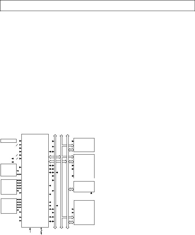
The functional block diagram on page 1 shows a block diagram of the ADSP-21160M, illustrating the following architectural features:
•Two processing elements, each made up of an ALU, Multiplier, Shifter, and Data Register File
•Data Address Generators (DAG1, DAG2)
•Program sequencer with instruction cache
•PM and DM buses capable of supporting four 32-bit data transfers between memory and the core every core processor cycle
•Interval timer
•On-Chip SRAM (4 Mbit)
•External port that supports:
•Interfacing to off-chip memory peripherals
•Glueless multiprocessing support for six ADSP-21160M SHARCs
•Host port
•DMA controller
•Serial ports and link ports
•JTAG test access port
Figure 1 shows a typical single-processor system. A multiprocessing system appears in Figure 4.
$'63 [
|
|
|
|
|
|
|
|
|
|
|
|
|
|
|
|
|
|
|
|
|
|
|
|
|
|
|
|
|
|
|
|
|
|
|
|
|
|
|
|
|
|
|
|
&/2&. |
|
|
&/.,1 |
|
|
%0 6 |
|
|
|
|
|
|
|
|
|
|
|
&6 |
|
%227 |
|
||||||||||||||||||||||
|
|
|
|
|
|
|
|
|
|
|
|
|
|
|
|
|
|
|
|
|
|
|
|
|
|
|
|
|
|
|
|
|
|
|
|
|
|||||||
|
|
|
|
|
|
&/.B& )* ± |
|
|
|
|
|
|
|
|
|
|
|
|
|
|
$''5 (3520 |
|
|||||||||||||||||||||
|
|
|
|
|
|
|
|
|
|
|
|
|
|
|
|
|
|
|
|
|
|||||||||||||||||||||||
|
|
|
|
|
|
|
|
|
|
|
|
|
|
|
|
|
|
|
|||||||||||||||||||||||||
|
|
|
|
|
|
|
(%227 |
|
&,) |
|
|
|
|
|
|
|
|
|
|
|
|
|
|
|
|
|
237,21$/ |
||||||||||||||||
|
|
|
|
|
|
|
|
|
|
|
|
|
|
|
|
|
|
|
|
|
|
|
|
|
|
|
|
|
|
|
|
|
|
||||||||||
|
|
|
|
|
|
|
/%227 |
|
|
|
|
|
|
|
|
|
|
|
|
|
|
|
|
|
|
|
|
|
'$7 |
$ |
|
|
|
||||||||||
|
|
|
|
|
|
|
|
|
%567 |
|
|
|
|
|
|
|
|
|
|
|
|
|
|
|
|
|
|
|
|
|
|||||||||||||
|
|
|
|
|
|
|
|
|
|
|
|
|
|
|
|
|
|
|
|
|
|
|
|||||||||||||||||||||
|
|
|
|
|
|
|
|
|
|
|
|
|
|
|
|
|
|
|
|
|
|
||||||||||||||||||||||
|
|
|
|
|
|
|
|
|
|
|
|
|
|
|
|
|
|
|
|
|
|
|
|
|
|
|
|
|
|
|
|
|
|
|
|
|
|
|
|
||||
|
|
|
|
|
|
,54 ± |
|
|
|
|
|
|
|
|
|
|
|
|
|
|
|
|
|
|
|
|
|
|
|
|
|
|
|
|
|
|
|||||||
|
|
|
|
|
|
|
$''5 ± |
|
|
|
|
|
|
|
$' '5 |
|
|
|
|||||||||||||||||||||||||
|
|
|
|
|
|
)/$* ± |
|
|
|
|
|
|
|
||||||||||||||||||||||||||||||
|
|
|
|
|
|
|
|
|
|
|
|
|
|
|
|
|
|
|
|
|
|
|
|
|
|
|
|
|
|
|
|
|
|
|
|
||||||||
|
|
|
|
|
|
|
|
|
|
'$7$ ± |
|
|
|
|
|
|
|
|
'$7 $ 0 (025< |
||||||||||||||||||||||||
|
|
|
|
|
|
|
|
|
7,0 (;3 |
|
|
|
|
|
|
|
|
|
|||||||||||||||||||||||||
|
|
|
|
|
|
|
|
|
|
|
|
|
|
|
|
|
|||||||||||||||||||||||||||
/,1. |
|
|
|
|
|
|
/;&/. |
|
|
|
5'; |
|
|
|
|
|
|
|
|
|
|
|
|
2( |
|
0 $33(' |
|||||||||||||||||
|
|
|
|
|
|
|
|
|
|
|
|
|
|
|
|
|
|
||||||||||||||||||||||||||
|
|
|
|
|
|
|
|
|
|
|
|
|
|
|
|
|
|
|
|
|
|
|
|
|
|
|
|
|
|||||||||||||||
'(9,&(6 |
|
|
|
|
|
|
|
|
|
|
|
|
|
|
|
|
|
|
|
|
|
|
|
|
|
|
|
|
|
:( |
|
'(9,&(6 |
|||||||||||
|
|
|
|
|
|
|
|
|
|
|
|
:5; |
|
|
|
|
|
|
|
|
|
|
|
|
|
|
|||||||||||||||||
|
|
|
|
|
|
/;$&. |
|
|
|
|
|
|
|
|
|
|
|
|
|
|
237,21$/ |
||||||||||||||||||||||
|
|
|
|
|
|
|
|
|
|
|
|
|
|
|
|
|
|
|
|
|
|
|
|
|
|
|
|||||||||||||||||
0 $; |
|
|
|
|
|
|
|
|
|
|
|
|
|
|
|
|
|
|
|
|
|
|
|
|
|
|
|
|
|
|
|
|
|
||||||||||
|
|
|
|
|
|
|
|
|
|
|
$&. |
|
|
|
|
|
|
|
|
|
|
|
|
|
$&. |
|
|
|
|||||||||||||||
237,21$/ |
|
|
|
|
|
|
|
/;'$7 ± |
|
|
|
|
|
|
|
|
|
|
|
|
|
|
|||||||||||||||||||||
|
|
|
|
|
|
|
|
|
|
|
|
|
|
|
|
|
|
|
|
|
|
|
|
|
|
|
|
||||||||||||||||
|
|
|
|
|
|
|
|
|
|
|
|
|
|
|
|
|
|
|
|
|
|
|
|
|
|
|
|
|
|
|
|
|
|
|
|
|
|||||||
|
|
|
|
|
|
|
|
|
|
|
|
|
|
|
|
|
|
|
|
|
|
|
|
|
|
|
|
|
&6 |
|
|
|
|
|
|||||||||
|
|
|
|
|
|
|
|
|
|
|
|
|
|
|
|
0 6 ± |
|
|
|
|
|
|
|
|
|
|
|
|
|||||||||||||||
|
|
|
|
|
|
|
|
|
|
|
|
|
|
|
|
|
|
|
|
|
|
|
|
|
|
|
|
|
|
|
|||||||||||||
|
|
|
|
|
|
|
|
|
|
56) |
|
|
|
|
|
|
|
|
|
|
|
|
|
|
|
&21752/ |
''5(66$ |
'$7$ |
|
|
|
|
|
|
|
|
|
|
|
||||
|
|
|
|
|
|
|
|
|
|
7&/. |
3$*( |
|
|
|
|
|
|
|
|
|
|
|
|
|
|
|
|
|
|
|
|
|
|||||||||||
|
|
|
|
|
|
|
|
|
|
|
|
|
|
|
|
|
|
|
|
|
|
|
|
|
|
|
|
|
|
||||||||||||||
6(5,$/ |
|
|
|
|
|
|
|
|
5&/ . |
|
|
|
|
|
|
|
|
|
|
|
|
|
|
|
|
|
'0 $ '(9,&( |
||||||||||||||||
|
|
|
|
|
|
|
|
|
|
|
|
|
|
|
|
|
|
|
|
|
|
|
|
|
|
|
|
|
|
|
|
|
|
||||||||||
6(5,$/ |
|
|
|
|
|
|
|
|
7)6 |
|
|
|
|
|
|
|
|
|
|
|
|
|
|
|
|
|
|
|
|
|
|
|
|
|
|
|
|
|
|
||||
|
|
|
|
|
|
|
|
6%76 |
|
|
|
|
|
|
|
|
|
|
|
|
|
|
|
|
|
|
|
|
|
||||||||||||||
'(9,&( |
|
|
|
|
|
|
|
|
|
|
|
|
|
|
|
|
|
|
|
|
|
|
|
|
|
237,21$/ |
|||||||||||||||||
'(9,&( |
|
|
|
|
|
|
|
|
|
|
|
|
|
|
|
|
|
|
|
|
|
|
|
|
|
|
|
|
|
|
|
|
|
|
|
|
|
|
|
|
|
|
|
237,21$/ |
|
|
|
|
|
|
|
|
|
|
|
|
|
|
|
|
|
|
|
|
|
|
|
|
|
|
|
|
|
|
'$7 |
$ |
|
|
|
||||||||
237,21$/ |
|
|
|
|
|
|
|
'7 |
&/.287 |
|
|
|
|
|
|
|
|
|
|
|
|
|
|
|
|
|
|
|
|
|
|||||||||||||
|
|
|
|
|
|
|
|
|
|
|
|
|
|
|
|
|
|
|
|
|
|
|
|
|
|
|
|
|
|
|
|||||||||||||
|
|
|
|
|
|
|
|
|
|
'5 |
|
|
|
|
|
|
|
|
|
|
|
|
|
|
|
|
|
|
|
|
|
|
|
|
|
|
|
|
|
|
|||
|
|
|
|
|
|
|
|
|
|
|
|
|
|
|
'0 $5 ± |
|
|
|
|
|
|
|
|
|
|
|
|
|
|
|
|
|
|||||||||||
|
|
|
|
|
|
|
|
|
|
|
|
|
|
|
|
|
|
|
|
|
|
|
|
|
|
|
|
|
|
|
|
|
|
|
|
|
|
||||||
|
|
|
|
|
|
|
|
|
|
7&/. |
'0 $* ± |
|
|
|
|
|
|
|
|
|
|
|
|
|
|
|
|
|
|
|
|||||||||||||
|
|
|
|
|
|
|
|
|
|
|
|
|
|
|
|
|
|
|
|
|
|
|
|
|
|
|
|
||||||||||||||||
|
|
|
|
|
|
|
|
|
|
|
|
|
|
|
|
|
|
|
|
|
|
|
|
|
|
|
|
|
|||||||||||||||
|
|
|
|
|
|
|
|
|
|
|
|
|
|
|
|
|
|
|
|
|
|
|
|
|
|
|
|
|
|
|
|
|
|
|
|
|
|
|
|
||||
|
|
|
|
|
|
|
|
|
|
5&/ . |
|
|
|
|
|
|
|
|
|
|
|
|
|
|
|
|
|
|
|
|
|
|
|
|
|
||||||||
6(5,$/ |
|
|
|
|
|
|
|
|
&6 |
|
|
|
|
|
|
|
|
|
|
|
|
|
|
|
|
|
|
|
|
|
|||||||||||||
|
|
|
|
|
|
|
|
|
|
|
|
|
|
|
|
|
|
|
|
|
|
|
|
||||||||||||||||||||
|
|
|
|
|
|
|
|
|
|
|
|
|
|
|
|
|
|
|
|
|
|
|
|
|
|
|
|
|
|
|
|
|
|
|
|
|
|
|
|
|
|
||
6(5,$/ |
|
|
|
|
|
|
|
|
7)6 |
|
|
|
|
|
|
|
|
|
|
|
|
|
|
|
|
|
|
|
|
|
|
|
|
|
|
+267 |
|
||||||
'(9,&( |
|
|
|
|
|
|
|
|
+%5 |
|
|
|
|
|
|
|
|
|
|
|
|
|
|
352&(6625 |
|||||||||||||||||||
|
|
|
|
|
|
|
|
|
|
|
|
|
|
|
|
|
|
|
|
|
|
|
|
|
|
||||||||||||||||||
'(9,&( |
|
|
|
|
|
|
|
|
56) |
|
|
|
|
|
|
|
|
|
|
|
|
|
|
|
|
|
|
|
|||||||||||||||
237,21$/ |
|
|
|
|
|
|
|
|
|
|
|
+%* |
|
|
|
|
|
|
|
|
|
|
|
|
|
|
,17(5)$&( |
|
|||||||||||||||
|
|
|
|
|
|
|
|
|
|
|
|
|
|
|
|
|
|
|
|
|
|
|
|
|
|
||||||||||||||||||
237,21$/ |
|
|
|
|
|
|
|
'7 |
|
|
|
|
|
|
|
|
|
|
|
|
|
|
|
||||||||||||||||||||
|
|
|
|
|
|
|
|
|
|
'5 |
5('< |
|
|
|
|
|
|
|
|
|
|
|
|
|
|
|
|
237,21$/ |
|||||||||||||||
|
|
|
|
|
|
|
|
|
|
|
|
|
|
|
|
|
|
|
|
|
|
|
|||||||||||||||||||||
|
|
|
|
|
|
|
|
|
|
|
|
|
|
|
|
|
|
|
|||||||||||||||||||||||||
|
|
|
|
|
|
|
|
|
|
|
|
|
|
|
|
|
|
|
|
|
|
|
|
|
|
|
|
||||||||||||||||
|
|
|
|
|
|
|
|
|
|
|
|
|
|
|
|
|
|
|
|
|
|
|
|
|
|
|
|
|
|
|
|
|
|
|
|
||||||||
|
|
|
|
|
|
|
53%$ |
|
|
|
|
|
%5 ± |
|
|
|
|
|
|
|
|
$''5 |
|
|
|
||||||||||||||||||
|
|
|
|
|
|
|
|
|
|
|
|
|
|
|
|
|
|
|
|
||||||||||||||||||||||||
|
|
|
|
|
|
|
|
|
|
|
|
|
|
|
|
|
|
|
|
|
|
|
|
|
|
|
|
|
|
|
|||||||||||||
|
|
|
|
|
|
|
|
|
|
,' ± |
|
|
|
|
|
|
|
|
|
|
|
|
|
|
|
|
|
|
|
|
|
|
|
|
|
|
|
|
|
|
|||
|
|
|
|
|
|
|
|
|
|
3$ |
|
|
|
|
|
|
|
|
|
|
|
|
|
|
'$7 |
$ |
|
|
|
||||||||||||||
|
|
|
|
|
|
|
|
|
|
|
|
|
|
|
|
|
|
|
|
|
|
|
|
|
|
||||||||||||||||||
|
|
|
|
|
|
|
|
|
|
|
|
|
|
|
|
|
|
|
|
|
|
|
|
|
|
|
|
|
|
|
|
|
|
|
|
||||||||
|
|
|
|
|
|
|
|
|
|
|
|
|
|
|
|
|
|
|
|
|
|
|
|
|
|
|
|
|
|
|
|
|
|
|
|
|
|
|
|
|
|
|
|
|
|
|
|
|
|
|
5(6(7 |
|
-7$* |
|
|
|
|
|
|
|
|
|
|
|
|
|
|
|
|
|
|
|
|
|
|
|
|||||||||||
|
|
|
|
|
|
|
|
|
|
|
|
|
|
|
|
|
|
|
|
|
|
|
|
|
|
|
|
|
|
|
|||||||||||||
Figure 1. Single-Processor System
ADSP-21160M
ADSP-21160M Family Core Architecture
The ADSP-21160M includes the following architectural features of the ADSP-2116x family core. The ADSP-21160M is code compatible at the assembly level with the ADSP-21060, ADSP-21061, and ADSP-21062.
SIMD Computational Engine
The ADSP-21160M contains two computational processing elements that operate as a Single Instruction Multiple Data (SIMD) engine. The processing elements are referred to as PEX and PEY, and each contains an ALU, multiplier, shifter, and register file. PEX is always active, and PEY may be enabled by setting the PEYEN mode bit in the MODE1 register. When this mode is enabled, the same instruction is executed in both processing elements, but each processing element operates on different data. This architecture is efficient at executing math-intensive DSP algorithms.
Entering SIMD mode also has an effect on the way data is transferred between memory and the processing elements. When in SIMD mode, twice the data bandwidth is required to sustain computational operation in the processing elements. Because of this requirement, entering SIMD mode also doubles the bandwidth between memory and the processing elements. When using the DAGs to transfer data in SIMD mode, two data values are transferred with each access of memory or the register file.
Independent, Parallel Computation Units
Within each processing element is a set of computational units. The computational units consist of an arithmetic/logic unit (ALU), multiplier, and shifter. These units perform single-cycle instructions. The three units within each processing element are arranged in parallel, maximizing computational throughput. Single multifunction instructions execute parallel ALU and multiplier operations. In SIMD mode, the parallel ALU and multiplier operations occur in both processing elements. These computation units support IEEE 32-bit single-precision floating-point, 40-bit extended precision floating-point, and 32-bit fixed-point data formats.
Data Register File
A general-purpose data register file is contained in each processing element. The register files transfer data between the computation units and the data buses, and store intermediate results. These 10-port, 32-register (16 primary, 16 secondary) register files, combined with the ADSP-2116x enhanced Harvard architecture, allow unconstrained data flow between computation units and internal memory. The registers in PEX are referred to as R0–R15 and in PEY as S0–S15.
Single-Cycle Fetch of Instruction and Four Operands
The ADSP-21160M features an enhanced Harvard architecture in which the data memory (DM) bus transfers data, and the program memory (PM) bus transfers both instructions and data (see the functional block diagram on page 1).
REV. 0 |
–3– |