

ADSP-2171/ADSP-2172/ADSP-2173
ADSP-2173–SPECIFICATIONS
RECOMMENDED OPERATING CONDITIONS
|
|
|
K Grade |
|
B Grade |
|
Parameter |
|
Min |
Max |
Min |
Max |
Unit |
|
|
|
|
|
|
|
VDD |
Supply Voltage |
3.0 |
3.6 |
3.0 |
3.6 |
V |
TAMB |
Ambient Operating Temperature |
0 |
+70 |
–40 |
+85 |
°C |
|
|
|
|
|
|
|
ELECTRICAL CHARACTERISTICS
|
|
|
K/B Grades |
|
|
Parameter |
|
Test Conditions |
Min |
Max |
Unit |
|
|
|
|
|
|
VIH |
Hi-Level Input Voltage1, 2 |
@ VDD = max |
2.0 |
|
V |
VIH |
Hi-Level CLKIN Voltage |
@ VDD = max |
2.0 |
|
V |
VIH |
Hi-Level RESET Voltage |
@ VDD = max |
2.2 |
|
V |
VIL |
Lo-Level Input Voltage1, 3 |
@ VDD = min |
|
0.4 |
V |
VOH |
Hi-Level Output Voltage1, 4, 5 |
@ VDD = min |
|
|
|
|
|
IOH = –0.5 mA |
2.4 |
|
V |
|
|
@ VDD = min |
|
|
|
|
Lo-Level Output Voltage1, 4, 5 |
IOH = –100 mA6 |
VDD – 0.3 |
|
V |
VOL |
@ VDD = min |
|
|
|
|
|
Hi-Level Input Current3 |
IOL = 2 mA |
|
0.4 |
V |
IIH |
@ VDD = max |
|
|
μA |
|
|
Lo-Level Input Current3 |
VIN = VDD max |
|
10 |
|
IIL |
@ VDD = max |
|
|
μA |
|
|
Tristate Leakage Current7 |
VIN = 0 V |
|
10 |
|
IOZH |
@ VDD = max, |
|
|
μA |
|
|
Tristate Leakage Current7 |
VIN = VDD max8 |
|
10 |
|
IOZL |
@ VDD = max, |
|
|
μA |
|
|
Supply Current (Idle)9, 10 |
VIN = 0 V8 |
|
10 |
|
IDD |
@ VDD = max |
|
7 |
mA |
|
IDD |
Supply Current (Dynamic)10 |
@ VDD = max |
|
|
|
|
|
tCK = 50 ns11 |
|
27 |
mA |
IDD |
Supply Current (Powerdown)10 |
Lowest Power Mode12 |
|
100 |
μA |
CI |
Input Pin Capacitance3, 6, 13 |
@ VIN = 2.5 V, |
|
|
|
|
|
fIN = 1.0 MHz, |
|
|
|
|
Output Pin Capacitance6, 7, 13, 14 |
TAMB = 25°C |
|
8 |
pF |
CO |
@ VIN = 2.5 V, |
|
|
|
|
|
|
fIN = 1.0 MHz, |
|
|
|
|
|
TAMB = 25°C |
|
8 |
pF |
NOTES
1Bidirectional pins: D0-D23, RFS0, RFS1, SCLK0, SCLK1, TFS0, TFS1, HD0-HD15/HAD0-HAD15.
2Input only pins: RESET, IRQ2, BR, MMAP, DR0, DR1, HSEL, HSIZE, BMODE, HMD0, HMD1, HRD/HWR, HWR/HDS, PWD, HA2/ALE, HA1-0.
3Input only pins: CLKIN, RESET, IRQ2, BR, MMAP, DR0, DR1, HSEL, HSIZE, BMODE, HMD0, HMD1, HRD/HWR, HWR/HDS, PWD, HA2/ALE, HA1-0. 4Output pins: BG, PMS, DMS, BMS, RD, WR, PWDACK, A0-A13, DT0, DT1, CLKOUT, HACK, FL2-0, BGH.
5Although specified for TTL outputs, all ADSP-2173 outputs are CMOS-compatible and will drive to V DD and GND, assuming no dc loads. 6Guaranteed but not tested.
7Three-statable pins: A0-A13, D0-D23, PMS, DMS, BMS, RD, WR, DT0, DT1, SCLK0, SCLK1, TFS0, TFS1, RFS0, RSF1, HD0-HD15/HAD0-HAD15. 80 V on BR, CLKIN Active (to force three-state condition).
9Idle refers to ADSP-2173 state of operation during execution of IDLE instruction. Deasserted pins are driven to either V DD or GND. Current reflects device operation with CLKOUT disabled.
10Current reflects device operating with no output loads.
11VIN = 0.4 V and 2.4 V. For typical figures for supply currents, refer to “Power Dissipation” section. 12See Chapter 9, of the ADSP-2100 Family User’s Manual for details.
13Applies to TQFP and PQFP package types.
14Output pin capacitance is the capacitve load for any three-state output pin. Specifications subject to change without notice.
REV. A |
–31– |
ADSP-2171/ADSP-2172/ADSP-2173
ADSP-2173 TIMING PARAMETERS
GENERAL NOTES
Use the exact timing information given. Do not attempt to derive parameters from the addition or subtraction of others. While addition or subtraction would yield meaningful results for an individual device, the values given in this data sheet reflect statistical variations and worst cases. Consequently, you cannot meaningfully add up parameters to derive longer times.
TIMING NOTES
Switching characteristics specify how the processor changes its signals. You have no control over this timing; it is dependent on the internal design. Timing requirements apply to signals that are controlled outside the processor, such as the data input for a read operation.
Timing requirements guarantee that the processor operates correctly with another device. Switching characteristics tell you what the device will do under a given circumstance. Also, use the switching characteristics to ensure any timing requirement of a device connected to the processor (such as memory) is satisfied.
MEMORY REQUIREMENTS
This chart links common memory device specification names and ADSP-2173 timing parameters for your convenience.
|
|
|
|
|
|
|
|
|
|
|
|
|
|
|
|
|
|
|
|
|
|
Common |
||
Parameter |
|
|
|
|
|
|
|
|
|
|
|
|
|
|
|
|
|
|
|
|
|
|
Memory Device |
|
Name |
|
Function |
Specification Name |
|||||||||||||||||||||
|
|
|
|
|
|
|
|
|
|
|
|
|
|
|
|
|
|
|
|
|
|
|
|
|
tASW |
A0-A13, |
|
|
|
|
|
, |
|
|
|
|
|
|
|
|
|
Address Setup to |
|||||||
DMS |
PMS |
|||||||||||||||||||||||
|
Setup before |
WR |
Low |
Write Start |
||||||||||||||||||||
tAW |
A0-A13, |
DMS |
, |
PMS |
|
|
|
Setup Address Setup |
||||||||||||||||
|
|
before |
WR |
Deasserted |
to Write End |
|||||||||||||||||||
tWRA |
A0-A13, |
DMS |
, |
PMS |
|
|
|
Address Hold Time |
||||||||||||||||
|
Hold after |
WR |
Deasserted |
|
|
|
||||||||||||||||||
tDW |
Data Setup before |
WR |
High |
|
Data Setup Time |
|||||||||||||||||||
tDH |
Data Hold after |
WR |
High |
Data Hold Time |
||||||||||||||||||||
tRDD |
|
RD |
Low to Data Valid |
|
OE |
to Data Valid |
||||||||||||||||||
tAA |
A0-A13, |
DMS |
, |
PMS |
, |
Address Access Time |
||||||||||||||||||
|
|
BMS |
to Data Valid |
|
|
|
||||||||||||||||||
|
|
|
|
|
|
|
|
|
|
|
|
|
|
|
|
|
|
|
|
|
|
|
|
|
–32– |
REV. A |
ADSP-2171/ADSP-2172/ADSP-2173
ADSP-2173
Parameter |
|
Min |
Max |
Unit |
|
|
|
|
|
Clock Signals |
|
|
|
|
tCK is defined as 0.5 tCKI. The ADSP-2173 uses an input clock with |
|
|
|
|
a frequency equal to half the instruction rate; a 10.0 MHz input |
|
|
|
|
clock (which is equivalent to 100 ns) yields a 50 ns processor cycle |
|
|
|
|
(equivalent to 20 MHz). tCK values within the range of 0.5 tCKI |
|
|
|
|
period should be substituted for all relevant timing parameters |
|
|
|
|
to obtain specification value. |
|
|
|
|
Example: tCKH = 0.5tCK – 10 ns = 0.5 (50 ns) – 10 ns = 15 ns. |
|
|
|
|
Timing Requirement: |
|
|
|
|
tCKI |
CLKIN Period |
100 |
160 |
ns |
tCKIL |
CLKIN Width Low |
20 |
|
ns |
tCKIH |
CLKIN Width High |
20 |
|
ns |
Switching Characteristic: |
|
|
|
|
tCKL |
CLKOUT Width Low |
0.5tCK – 10 |
|
ns |
tCKH |
CLKOUT Width High |
0.5tCK – 10 |
|
ns |
tCKOH |
CLKIN High to CLKOUT High |
0 |
25 |
ns |
Control Signals |
|
|
|
|
Timing Requirement: |
5tCK1 |
|
|
|
tRSP |
RESET Width Low |
|
ns |
|
NOTE
1Applies after power-up sequence is complete. Internal phase lock loop requires no more than 2000 CLKIN cycles assuming stable CLKIN (not including crystal oscillator start-up time).
tCKI
tCKIH
CLKIN
tCKIL
tCKOH
tCKH
CLKOUT
tCKL
Figure 24. Clock Signals
REV. A |
–33– |
ADSP-2171/ADSP-2172/ADSP-2173
ADSP-2173
Parameter |
|
|
Min |
Max |
Unit |
|
|
|
|
|
|
Interrupts and Flags |
|
|
|
||
Timing Requirement: |
|
|
|
||
tIFS |
|
or FI Setup before CLKOUT Low1, 2, 3 |
0.25tCK + 23 |
|
ns |
IRQx |
|
||||
tIFH |
IRQx |
or FI Hold after CLKOUT High1, 2, 3 |
0.25tCK |
|
ns |
Switching Characteristic: |
|
|
|
||
tFOH |
Flag Output Hold after CLKOUT Low4 |
0.5tCK – 10 |
|
ns |
|
tFOD |
Flag Output Delay from CLKOUT Low4 |
|
0.5tCK + 5 |
ns |
|
NOTES
1If IRQx and FI inputs meet tIFS and tIFH setup/hold requirements, they will be recognized during the current clock cycle; otherwise the signals will be recognized on the following cycle. (Refer to “Interrupt Controller Operation” in the Program Control chapter of the User’s Manual for further information on interrupt servicing.) 2Edge-sensitive interrupts require pulse widths greater than 10 ns; level-sensitive interrupts must be held low until serviced.
3IRQx = IRQ0, IRQ1, and IRQ2.
4Flag Output = FL0, FL1, FL2, and FO.
tFOD
CLKOUT
tFOH
FLAG
OUTPUTS
tIFH
IRQx
FI
tIFS
Figure 25. Interrupts and Flags
–34– |
REV. A |
ADSP-2171/ADSP-2172/ADSP-2173
ADSP-2173
Parameter |
|
|
|
|
|
|
|
|
|
|
|
|
|
|
|
|
|
|
|
|
|
|
|
|
|
|
|
|
|
|
|
|
|
|
|
|
|
|
Min |
Max |
Unit |
|
|
|
|
|
|
|
|
|
|
|
|
|
|
|
|
|
|
|
|
|
|
|
|
|
|
|
|
|
|
|
|
|
|
|
|
|
|
|
|
|
|
Bus Request/Grant |
|
|
|
||||||||||||||||||||||||||||||||||||||
Timing Requirement: |
|
|
|
||||||||||||||||||||||||||||||||||||||
tBH |
|
|
|
|
Hold after CLKOUT High1 |
0.25tCK + 2 |
|
ns |
|||||||||||||||||||||||||||||||||
BR |
|
||||||||||||||||||||||||||||||||||||||||
tBS |
BR |
|
|
|
Setup before CLKOUT Low1 |
0.25tCK + 22 |
|
ns |
|||||||||||||||||||||||||||||||||
Switching Characteristic: |
|
|
|
||||||||||||||||||||||||||||||||||||||
tSD |
CLKOUT High to |
|
|
|
|
|
|
|
, |
|
|
|
|
|
, |
|
|
, |
|
0.25tCK + 16 |
ns |
||||||||||||||||||||
DMS |
PMS |
BMS |
|
||||||||||||||||||||||||||||||||||||||
|
RD |
, |
WR |
Disable |
|
|
|
||||||||||||||||||||||||||||||||||
tSDB |
DMS |
, |
PMS |
, |
BMS |
|
, |
RD |
, |
|
WR |
|
|
|
|
|
|
||||||||||||||||||||||||
|
Disable to |
BG |
|
Low |
0 |
|
ns |
||||||||||||||||||||||||||||||||||
tSE |
BG |
|
High to |
DMS |
, |
PMS |
, |
BMS |
, |
|
|
|
|
||||||||||||||||||||||||||||
|
RD |
, |
WR |
Enable |
0 |
|
ns |
||||||||||||||||||||||||||||||||||
tSEC |
DMS |
, |
PMS |
, |
BMS |
, |
RD |
, |
WR |
|
|
|
|
|
|||||||||||||||||||||||||||
|
Enable to CLKOUT High |
0.25tCK – 10 |
|
ns |
|||||||||||||||||||||||||||||||||||||
tSDBH |
DMS |
, |
PMS |
, |
BMS |
, |
RD |
, |
WR |
|
|
|
|
|
|||||||||||||||||||||||||||
|
Disable to |
BGH |
Low2 |
0 |
|
ns |
|||||||||||||||||||||||||||||||||||
tSEH |
BGH |
High to |
DMS |
, |
PMS |
, |
BMS |
, |
|
|
|
||||||||||||||||||||||||||||||
|
RD |
, |
WR |
Enable2 |
0 |
|
ns |
||||||||||||||||||||||||||||||||||
NOTES
1BR is an asynchronous signal. If BR meets the setup/hold requirements, it will be recognized during the current clock cycle; otherwise the signal will be recognized on the following cycle. Refer to the ADSP-2100 Family User’s Manual for BR/BG cycle relationships.
2BGH is asserted when the bus is granted and the processor requires control of the bus to continue.
tBH
CLKOUT
BR
|
|
tBS |
CLKOUT |
|
|
PMS, DMS |
|
|
BMS, RD |
tSD |
tSEC |
WR |
||
BG |
|
tSDB |
|
|
tSE |
BGH |
|
tSDBH |
tSEH
Figure 26. Bus Request–Bus Grant
REV. A |
–35– |
ADSP-2171/ADSP-2172/ADSP-2173
ADSP-2173
Parameter |
|
|
|
|
|
|
|
|
|
|
|
|
|
|
|
|
|
|
|
|
|
|
|
|
|
Min |
Max |
Unit |
|
|
|
|
|
|
|
|
|
|
|
|
|
|
|
|
|
|
|
|
|
|
|
|
|
|
|
|
|
Memory Read |
|
|
|
|
|
|
|
|
|
|
|
|
|
|
|
|
|
|
|
|
|
|
|
|
|
|
|
|
Timing Requirement: |
|
|
|
|||||||||||||||||||||||||
tRDD |
|
Low to Data Valid |
|
0.5tCK – 15 + w |
ns |
|||||||||||||||||||||||
RD |
|
|||||||||||||||||||||||||||
tAA |
A0–A13, |
PMS |
, |
DMS |
, |
BMS |
|
to Data Valid |
|
0.75tCK – 20.5 + w |
ns |
|||||||||||||||||
tRDH |
Data Hold from |
RD |
High |
0 |
|
ns |
||||||||||||||||||||||
Switching Characteristic: |
|
|
|
|||||||||||||||||||||||||
tRP |
|
Pulse Width |
0.5tCK – 5 + w |
|
ns |
|||||||||||||||||||||||
RD |
|
|||||||||||||||||||||||||||
tCRD |
CLKOUT High to |
RD |
|
Low |
0.25tCK – 5 |
0.25tCK + 10 |
ns |
|||||||||||||||||||||
tASR |
A0–A13, |
PMS |
, |
DMS |
, |
BMS |
|
Setup before |
RD |
Low |
0.25tCK – 7 |
|
ns |
|||||||||||||||
tRDA |
A0–A13, |
PMS |
, |
DMS |
, |
BMS |
Hold after |
RD |
Deasserted |
0.25tCK – 3 |
|
ns |
||||||||||||||||
tRWR |
RD |
High to |
RD |
or |
WR |
Low |
0.5tCK – 5 |
|
ns |
|||||||||||||||||||
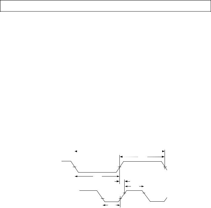
w = wait states x tCK.
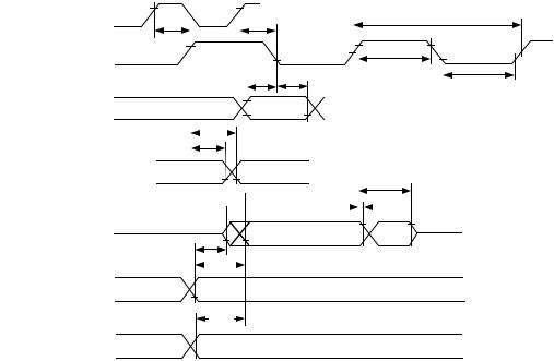
CLKOUT
A0–A13
DMS, PMS
BMS
|
|
|
|
|
|
|
|
|
|
|
|
tRDA |
|
|
|
|
|
|
|
|
|
|
|
|
|
|
|
|
|
|
|
RD |
|
|
|
|
|||||||||||
|
|
|
|
|
|
|
|
|
|
|
|
|
|
||
|
|
|
tASR |
|
|
|
|
||||||||
|
|
|
|
|
|
|
|
|
tRP |
|
|
|
|
|
|
|
|
|
t |
||||||||||||
|
|
|
|
|
|
|
|
|
|
|
|
||||
|
|
tCRD |
|
|
|
|
|
|
|
||||||
|
|
|
|
|
|
|
|
|
|
RWR |
|||||
|
|
|
|
|
|||||||||||
|
|
|
|
|
|||||||||||
|
|
|
|
|
|
|
|
|
|
|
|||||
D |
|
|
|
|
|||||||||||
|
|
|
|
|
|
|
|
|
|
|
|
|
|||
|
|
|
|
|
|
|
|
tRDD |
|
||||||
|
|
|
|
|
|
|
|
|
|
|
tRDH |
||||
|
|
|
|
tAA |
|
|
|
|
|
|
|
||||
|
|
|
|
|
|
|
|
|
|
|
|
|
|||
WR
Figure 27. Memory Read
–36– |
REV. A |
ADSP-2171/ADSP-2172/ADSP-2173
ADSP-2173
Parameter |
|
|
|
|
|
|
|
|
|
|
|
|
|
|
|
|
|
|
|
|
|
|
|
|
|
|
|
|
Min |
Max |
Unit |
|
|
|
|
|
|
|
|
|
|
|
|
|
|
|
|
|
|
|
|
|
|
|
|
|
|
|
|
|
|
|
|
Memory Write |
|
|
|
|
|
|
|
|
|
|
|
|
|
|
|
|
|
|
|
|
|
|
|
|
|
|
|
|
|
|
|
Switching Characteristic: |
|
|
|
||||||||||||||||||||||||||||
tDW |
Data Setup before |
|
|
|
|
|
|
|
High |
0.5 tCK – 7 + w |
|
ns |
|||||||||||||||||||
WR |
|
||||||||||||||||||||||||||||||
tDH |
Data Hold after |
WR |
|
High |
0.25tCK – 2 |
|
ns |
||||||||||||||||||||||||
tWP |
WR |
Pulse Width |
0.5tCK – 5 + w |
|
ns |
||||||||||||||||||||||||||
tWDE |
WR |
Low to Data Enabled |
0 |
|
ns |
||||||||||||||||||||||||||
tASW |
A0–A13, |
DMS |
, |
|
PMS |
|
Setup before |
WR |
Low |
0.25tCK – 7 |
|
ns |
|||||||||||||||||||
tDDR |
Data Disable before |
WR |
or |
RD |
Low |
0.25tCK – 7 |
|
ns |
|||||||||||||||||||||||
tCWR |
CLKOUT High to |
WR |
|
Low |
0.25tCK – 5 |
0.25 tCK + 10 |
ns |
||||||||||||||||||||||||
tAW |
A0–A13, |
DMS |
|
, |
PMS |
, Setup before |
WR |
Deasserted |
0.75tCK – 11.5 + w |
|
ns |
||||||||||||||||||||
tWRA |
A0–A13, |
DMS |
|
, |
PMS |
Hold after |
WR |
Deasserted |
0.25tCK – 3 |
|
ns |
||||||||||||||||||||
tWWR |
WR |
High to |
RD |
or |
WR |
Low |
0.5tCK – 5 |
|
ns |
||||||||||||||||||||||
w = wait states x tCK.
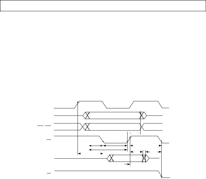
CLKOUT
A0–A13
DMS, PMS
 tWRA
tWRA 
WR
tCWR
tAS W |
|
|
|
tWP |
|
tWWR |
|
|
|
tAW |
|
|
tDH |
|
tDD R |
|
|
|
|
|
|
D


 tDW tWDE
RD
Figure 28. Memory Write
REV. A |
–37– |
ADSP-2171/ADSP-2172/ADSP-2173
ADSP-2173
Parameter |
|
|
|
|
|
Min |
|
|
Max |
Unit |
|||
|
|
|
|
|
|
|
|
|
|
|
|
|
|
Serial Ports |
|
|
|
|
|
|
|
|
|
|
|
|
|
Timing Requirement: |
|
|
|
|
|
|
|
|
|
|
|
|
|
tSCK |
SCLK Period |
|
|
|
|
76.9 |
|
|
|
|
|
ns |
|
tSCS |
DR/TFS/RFS Setup before SCLK Low |
|
8 |
|
|
|
|
|
|
ns |
|||
tSCH |
DR/TFS/RFS Hold after SCLK Low |
|
10 |
|
|
|
|
|
|
ns |
|||
tSCP |
SCLKIN Width |
|
|
|
|
28 |
|
|
|
|
|
|
ns |
Switching Characteristic: |
|
|
|
|
|
|
|
|
|
|
|
|
|
tCC |
CLKOUT High to SCLKOUT |
|
0.25tCK |
|
|
0.25tCK + 15 |
ns |
||||||
tSCDE |
SCLK High to DT Enable |
|
|
|
|
0 |
|
|
|
|
|
|
ns |
tSCDV |
SCLK High to DT Valid |
|
|
|
|
|
|
|
20 |
ns |
|||
tRH |
TFS/RFSOUT Hold after SCLK High |
|
0 |
|
|
|
|
|
|
ns |
|||
tRD |
TFS/RFSOUT Delay from SCLK High |
|
|
|
|
20 |
ns |
||||||
tSCDH |
DT Hold after SCLK High |
|
|
|
|
0 |
|
|
|
|
|
|
ns |
tTDE |
TFS(Alt) to DT Enable |
|
|
|
|
0 |
|
|
|
|
|
|
ns |
tTDV |
TFS(Alt) to DT Valid |
|
|
|
|
|
|
|
19 |
ns |
|||
tSCDD |
SCLK High to DT Disable |
|
|
|
|
|
|
|
25 |
ns |
|||
tRDV |
RFS (Multichannel, Frame Delay Zero) to DT Valid |
|
|
|
20 |
ns |
|||||||
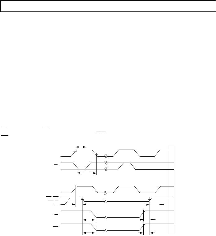
|
CLKOUT |
tCC |
tCC |
|
|
|
|
|
|
|
|
||
|
|
|
|
|
tSCK |
|
|
|
|
||||
|
|
|
|
|
|
|
|
|
|
|
|
|
|
|
SCLK |
|
|
|
|
|
|
|
|
|
|
|
|
|
|
|
|
|
|
tSCP |
|
|
|
|
|
|
|
|
|
|
|
|
|
|
|
|
|
|
|
|
|
|
|
|
|
|
tSCS tSCH |
|
|
|
|
|
|
|
|
|
|
|
|
|
|
|
|
|
|
tSCP |
|
||
|
DR |
|
|
|
|
|
|
|
|
|
|
|
|
|
RFSIN |
|
|
|
|
|
|
|
|
|
|
|
|
|
TFSIN |
|
|
|
|
|
|
|
|
|
|
|
|
|
|
|
tRD |
|
|
|
|
|
|
|
|
|
|
|
|
|
tRH |
|
|
|
|
|
|
|
|
|
|
|
RFSOUT |
|
|
|
|
|
|
|
|
|
|
|
|
|
TFSOUT |
|
|
|
|
tSCDD |
|
|
|
|
|
||
tSCDV 

tSCDE 
 tSCDH
tSCDH 
DT
tTDE tTDV
TFS
ALTERNATE
FRAME MODE
tRDV
RFS
MULTICHANNEL MODE, FRAME DELAY 0 (MFD = 0)
Figure 29. Serial Ports
–38– |
REV. A |
ADSP-2171/ADSP-2172/ADSP-2173
ADSP-2173
Parameter |
|
|
|
|
|
|
|
|
|
|
|
|
|
|
|
|
|
|
|
|
|
|
|
Min |
Max |
Unit |
|||||||
|
|
|
|
|
|
|
|
|
|
|
|
|
|
|
|
|
|
|
|
|
|
|
|
|
|
|
|
|
|
|
|
|
|
Host Interface Port |
|
|
|
|
|
|
|
|
|
|
|||||||||||||||||||||||
Separate Data and Address (HMD1 = 0) |
|
|
|
|
|
|
|
|
|
|
|||||||||||||||||||||||
Read Strobe and Write Strobe (HMD0 = 0) |
|
|
|
|
|
|
|
|
|
|
|||||||||||||||||||||||
Timing Requirement: |
|
|
|
|
|
|
|
|
|
|
|||||||||||||||||||||||
tHSU |
HA2–0 Setup before Start of Write or Read1, 2 |
|
8 |
|
ns |
||||||||||||||||||||||||||||
tHDSU |
Data Setup before End of Write3 |
|
|
|
|
|
|
|
8 |
|
ns |
||||||||||||||||||||||
tHWDH |
Data Hold after End of Write3 |
|
|
|
|
|
|
|
3 |
|
ns |
||||||||||||||||||||||
tHH |
HA2–0 Hold after End of Write or Read3, 4 |
|
3 |
|
ns |
||||||||||||||||||||||||||||
tHRWP |
Read or Write Pulse Width5 |
|
|
|
|
|
|
|
30 |
|
ns |
||||||||||||||||||||||
Switching Characteristic: |
|
|
|
|
|
|
|
|
|
|
|||||||||||||||||||||||
tHSHK |
|
|
|
|
|
|
Low after Start of Write or Read1, 2 |
|
0 |
20 |
ns |
||||||||||||||||||||||
HACK |
|||||||||||||||||||||||||||||||||
tHKH |
HACK |
|
Hold after End of Write or Read3, 4 |
|
0 |
20 |
ns |
||||||||||||||||||||||||||
tHDE |
Data Enabled after Start of Read2 |
|
|
|
|
|
|
|
0 |
|
ns |
||||||||||||||||||||||
tHDD |
Data Valid after Start of Read2 |
|
|
|
|
|
|
|
|
23 |
ns |
||||||||||||||||||||||
tHRDH |
Data Hold after End of Read4 |
|
|
|
|
|
|
|
0 |
|
ns |
||||||||||||||||||||||
tHRDD |
Data Disabled after End of Read4 |
|
|
|
|
|
|
|
|
15 |
ns |
||||||||||||||||||||||
NOTES |
|
|
|
|
|
|
|
|
|
|
|
|
|
|
|
|
|
|
|
|
|
|
|
|
|
|
|||||||
1Start of Write = |
HWR |
Low and |
HSEL |
Low. |
|
|
|
|
|
|
|
|
|
|
|||||||||||||||||||
2Start of Read = |
HRD |
|
Low and |
HSEL |
Low. |
|
|
|
|
|
|
|
|
|
|
||||||||||||||||||
3End of Write = |
HWR |
High or |
HSEL |
High. |
|
|
|
|
|
|
|
|
|
|
|||||||||||||||||||
4End of Read = |
HRD |
|
High or |
HSEL |
|
High. |
|
|
|
|
|
|
|
|
|
|
|||||||||||||||||
5Read Pulse Width = |
HRD |
Low and |
HSEL |
Low, Write Pulse Width = |
HWR |
Low and |
HSEL |
Low. |
|
|
|
||||||||||||||||||||||
|
|
|
|
|
|
|
|
|
|
|
|
|
|
|
|
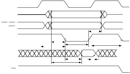
HA2–0 |
ADDRESS |
|
|
|
|||||||||||||
|
|
|
|
|
|
|
|
|
|
|
|
|
|
|
|
|
|
|
|
|
|
|
|
|
|
|
|
|
|
|
|||
|
|
|
|
|
|
|
|
|
|
|
|
|
|
|
|
|
|
|
|
|
|
|
|
|
tHRWP |
|
|
|
|||||
|
|
|
|
|
|
|
|
|
|
|
|
|
|
|
|
|
HSEL |
|
|
|
|||||||||||||
|
|
|
|
|
|
|
|
|
|
|
|
|
|
|
|
|
|
|
|
|
|
|
|
|
|
|
|||||||
|
|
|
|
|
|
|
|
|
|
|
|
|
|
|
|
|
|
|
|
|
|
|
|
|
|
|
|||||||
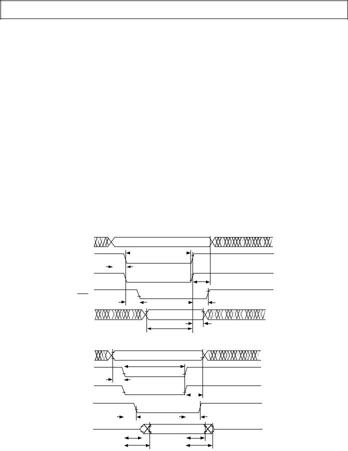
Host Write Cycle
tHSU
HWR |
tHH |
HACK
tHSHK |
|
tHKH |
Host Read Cycle
HD15–0 |
|
|
DATA |
|
||||||
|
|
|
|
|
|
|
|
|
|
tHWDH |
|
|
|
|
|
|
|
|
tHDSU |
|
|
|
|
|
|
|
|
|
|
|
|
|
HA2–0 |
|
ADDRESS |
|
|||||||
|
|
|
|
|
|
|
|
|
|
|
|
|
|
|
|
|
|
tHRWP |
|
||
|
|
HSEL |
|
|||||||
|
|
|
|
|
|
|
||||
|
|
tHSU |
|
|||||||
|
|
|
|
|
|
|
||||
|
|
|
|
|
|
|
|
|
|
tHH |
|
|
|
HRD |
|
|
|
|
|||
|
|
|
|
|
|
|
|
|||
|
HACK |
|
|
|
|
|
||||
|
|
|
|
|
|
|
tHSHK |
tHKH |
||
HD15–0 |
DATA |
|
tHDE |
t |
HRDH |
|
|
|
tHDD |
tHRDD |
|
Figure 30. Host Interface Port (HMD1 = 0, HMD0 = 0)
REV. A |
–39– |
ADSP-2171/ADSP-2172/ADSP-2173
ADSP-2173
Parameter |
|
|
Min |
Max |
Unit |
|
|
|
|
|
|
Host Interface Port |
|
|
|
||
Separate Data and Address (HMD1 = 0) |
|
|
|
||
Read Strobe and Write Strobe (HMD0 = 1) |
|
|
|
||
Timing Requirement: |
|
|
|
||
tHSU |
HA2–0, HRW Setup before Start of Write or Read1 |
8 |
|
ns |
|
tHDSU |
Data Setup before End of Write2 |
8 |
|
ns |
|
tHWDH |
Data Hold after End of Write2 |
3 |
|
ns |
|
tHH |
HA2–0, HRW Hold after End of Write or Read2 |
3 |
|
ns |
|
tHRWP |
Read or Write Pulse Width3 |
30 |
|
ns |
|
Switching Characteristic: |
|
|
|
||
tHSHK |
|
Low after Start of Write or Read1 |
0 |
20 |
ns |
HACK |
|||||
tHKH |
HACK |
Hold after End of Write or Read2 |
0 |
20 |
ns |
tHDE |
Data Enabled after Start of Read1 |
0 |
|
ns |
|
tHDD |
Data Valid after Start of Read1 |
|
23 |
ns |
|
tHRDH |
Data Hold after End of Read2 |
0 |
|
ns |
|
tHRDD |
Data Disabled after End of Read2 |
|
15 |
ns |
|
NOTES
1Start of Write or Read = HDS Low and HSEL Low. 2End of Write or Read = HDS High and HSEL High. 3Read or Write Pulse Width = HDS Low and HSEL Low.
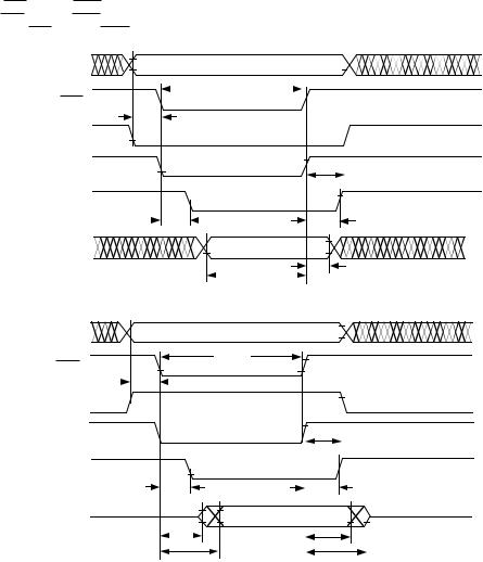
Host Write Cycle
Host Read Cycle
HA2–0 |
ADDRESS |
tHRWP
HSEL
tHSU
HRW
|
|
HDS |
|
|
|
|
tHH |
|
|
|
|
|
|
|
|
|
|
HACK |
|
|
|
|
||||
|
|
|
|
|
tHSHK |
tHKH |
||
HD15–0 |
|
DATA |
|
|||||
|
|
|
|
|
|
|
|
tHWDH |
|
|
|
|
|
|
tHDSU |
|
|
|
|
|
|
|
|
|
|
|
HA2–0 |
ADDRESS |
|
||||||
tHRWP
HSEL
tHSU
HRW
|
|
|
|
|
|
|
|
|
tHH |
|
|
HDS |
|
|
|||||
|
|
|
|
|
|
|
|
||
HACK |
|
|
|
|
|
||||
|
|
|
|
tHSHK |
|
|
|
|
tHKH |
HD15–0 |
DATA |
||||||||
|
|
|
|
tHDE |
|
|
|
|
|
|
|
|
|
|
tHRDH |
||||
|
|
|
|
tHDD |
|
|
|
|
|
|
|
|
|
|
t |
HRDD |
|
||
Figure 31. Host Interface Port (HMD1 = 0, HMD0 = 1)
–40– |
REV. A |