

ADSP-2171/ADSP-2172/ADSP-2173
|
|
|
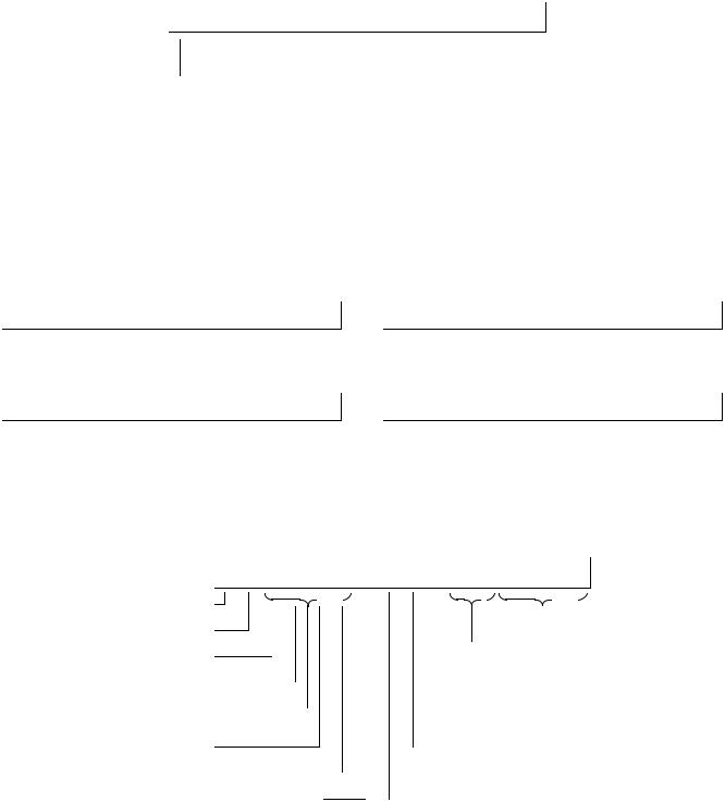
ASTAT |
|
|
|
|
|
|
SSTAT (Read-Only) |
|||||||
7 |
6 |
5 |
4 |
3 |
2 |
1 |
0 |
|
7 |
6 |
5 |
4 |
3 |
2 |
1 |
0 |
|
|
|
|
|
|
|
|
|
|
|
|
|
|
|
|
|
|
|
0 |
0 |
0 |
0 |
0 |
0 |
0 |
0 |
|
0 |
1 |
0 |
1 |
0 |
1 |
0 |
1 |
|
|
|
|
|
|
|
|
|
AZ ALU Result Zero |
|
|
|
|
|
|
|
|
PC Stack Empty |
|
|
|
|
|
|
|
|
|
|
|
|
|
|
|
|
||
|
|
|
|
|
|
|
|
AN ALU Result Negative |
|
|
|
|
|
|
|
|
PC Stack Overflow |
|
|
|
|
|
|
|
|
AV ALU Overflow |
|
|
|
|
|
|
|
|
Count Stack Empty |
|
|
|
|
|
|
|
|
AC ALU Carry |
|
|
|
|
|
|
|
|
Count Stack Overflow |
|
|
|
|
|
|
|
|
AS ALU X Input Sign |
|
|
|
|
|
|
|
|
Status Stack Empty |
|
|
|
|
|
|
|
|
AQ ALU Quotient |
|
|
|
|
|
|
|
|
Status Stack Overflow |
|
|
|
|
|
|
|
|
MV MAC Overflow |
|
|
|
|
|
|
|
|
Loop Stack Empty |
|
|
|
|
|
|
|
|
SS Shifter Input Sign |
|
|
|
|
|
|
|
|
Loop Stack Overflow |
MSTAT
6 |
5 |
4 |
3 |
2 |
1 |
0 |
0 |
0 |
0 |
0 |
0 |
0 |
0 |
|
|
|
|
|
|
|
 Data Register Bank Select 0 = primary, 1 = secondary
 Bit Reverse Mode Enable (DAG1)
 ALU Overflow Latch Mode Enable
 AR Saturation Mode Enable
 MAC Result Placement
0 = fractional, 1 = integer
 Timer Enable
 Go Mode Enable
System Control Register
0x3FFF
15 |
14 |
|
13 |
12 |
11 |
10 |
9 |
8 |
7 |
|
6 |
5 |
4 |
|
3 |
2 |
1 |
|
0 |
|
||||
|
|
|
|
|
|
|
|
|
|
|
|
|
|
|
|
|
|
|
|
|
|
|
|
|
|
0 |
0 |
|
0 |
0 |
0 |
1 |
0 |
0 |
0 |
|
0 |
1 |
|
1 |
|
1 |
1 |
|
1 |
|
1 |
|
|
|
|
|
|
|
|
|
|
|
|
|
|
|
|
|
|
|
|
|
|
|
|
|
|
|
|
|
|
|
|
|
|
|
|
|
|
|
|
|
|
|
|
|
|
|
|
|
|
|
|
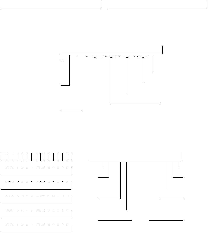
SPORT0 Enable |
|
|
|
|
|
|
|
|
|
|
|
|
|
|
|
|
PWAIT |
|
|
|||||
1 = enabled, 0 = disabled |
|
|
|
|
|
|
|
|
|
|
|
|
|
|
|
|
|
|
||||||
|
|
|
|
|
|
|
|
|
|
|
|
|
|
|
|
Program Memory |
||||||||
|
|
|
|
|
|
|
|
|
|
|
|
|
|
|
|
|
|
|
|
|||||
SPORT1 Enable |
|
|
|
|
|
|
|
|
|
|
|
BWAIT |
|
|
Wait States |
|||||||||
|
|
|
|
|
|
|
|
|
|
|
|
|
|
|
|
|
|
|||||||
1 = enabled, 0 = disabled |
|
|
|
|
|
|
|
|
|
|
|
|
|
|
|
|
|
|
||||||
|
|
|
|
|
|
|
|
|
|
|
Boot Wait States |
|
|
|||||||||||
|
|
|
|
|
|
|
|
|
|
BPAGE |
|
|
|
|
||||||||||
SPORT1 Configure |
|
|
|
|
|
|
|
|
|
|
|
|
|
|
|
|
|
|
||||||
|
|
|
|
|
|
Boot Page Select |
|
|
|
|
|
|
|
|||||||||||
1 = serial port |
|
|
|
|
|
|
|
|
|
|
|
|
|
|
|
|
|
|
|
|
|
|||
0 = FI, FO, IRQ0, IRQ1, SCLK |
BFORCE |
|
Boot Force Bit |
||
|
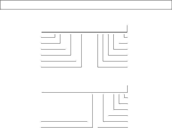
Timer Registers
15 |
14 |
13 |
12 |
11 |
10 |
9 |
8 |
7 |
6 |
5 |
4 |
3 |
2 |
1 |
0 |
|
||||
|
|
|
|
|
|
|
|
|
|
|
|
|
|
|
|
|
|
|
0x3FFD |
|
|
|
|
|
|
|
|
|
|
|
|
|
|
|
|
|
|
|
|
|
|
|
|
|
|
|
|
|
|
TPERIOD |
Period |
Register |
|
|
|
|
|
|||||
|
|
|
|
|
|
|
|
|
|
|
|
|
|
|
|
|
|
|
0x3FFC |
|
|
|
|
|
|
|
|
|
|
|
|
|
|
|
|
|
|
|
|
||
|
|
|
|
|
|
|
|
|
|
|
|
|
|
|
||||||
|
|
|
|
|
|
|
|
|
|
|
|
|
|
|
|
|
|
|
|
|
|
|
|
|
|
|
|
|
TCOUNT |
Counter |
Register |
|
|
|
|
|
|||||
|
|
|
|
|
|
|
|
|
|
|
|
|
|
|
|
|
|
0x3FFB |
||
|
|
|
|
|
|
|
|
|
|
|
|
|
|
|
|
|
|
|
|
|
|
|
|
|
|
|
|
|
|
|
|
||||||||||
|
|
|
|
|
|
|
|
|
|
|
|
|
|
|
|
|
|
|||
0 |
0 |
0 |
0 |
0 |
|
0 |
0 |
0 |
|
|
TSCALE |
Scaling |
Register |
|
||||||
|
|
|
|
|
|
|
|
|
|
|
|
|
|
|
|
|
|
|
|
|
|
|
|
|
|
|
|
|
|
|
|
|
|
|
|
|
|
|
|
|
|
Control Registers
REV. A |
–11– |
ADSP-2171/ADSP-2172/ADSP-2173
ROM Enable/Data Memory Wait State
Control Register
0x3FFE
15 |
14 |
13 |
12 |
11 |
10 |
9 |
8 |
7 |
6 |
5 |
4 |
3 |
2 |
1 |
0 |
|
0 |
1 |
1 |
1 |
1 |
1 |
1 |
1 |
1 |
1 |
1 |
1 |
1 |
1 |
1 |
1 |
|
|
|
|
|
|
|
|
|
|
|
|
|
|
|
|
|
|
|
DWAIT4 |
|
DWAIT3 |
DWAIT2 |
DWAIT1 |
DWAIT0 |
||||||||||
|
|
|
|
ROM enable |
|
|
|
|
|
|
|
|
|
|||
|
|
|
|
1 |
= enable |
|
|
|
|
|
|
|
|
|
||
|
|
|
|
0 |
= disable |
|
|
|
|
|
|
|
|
|
||
SPORT0 Multichannel Receive Word Enable Registers
1 = Channel Enabled
0 = Channel Ignored
0x3FFA
31 30 29 28 27 26 25 24 23 22 21 20 19 18 17 16
SPORT0 Multichannel Transmit Word Enable Registers
1 = Channel Enabled
0 = Channel Ignored
0x3FF8
31 30 29 28 27 26 25 24 23 22 21 20 19 18 17 16
|
|
|
|
|
|
|
|
|
|
|
|
|
|
|
|
|
|
|
|
|
|
|
|
|
|
|
|
|
|
|
|
|
|
|
|
|
|
|
|
|
|
0x3FF9 |
|
|
|
|
|
|
|
|
|
|
|
|
|
|
|
0x3FF7 |
|
|
|
|
|
|
|
||||
15 |
14 |
13 |
12 |
11 |
10 |
9 |
8 |
7 |
|
6 |
5 |
4 |
3 |
2 |
1 |
0 |
15 |
14 |
13 |
12 |
11 |
10 |
9 |
8 |
7 |
|
6 |
5 |
4 |
3 |
2 |
1 |
0 |
|
|
|
|
|
|
|
|
|
|
|
|
|
|
|
|
|
|
|
|
|
|
|
|
|
|
|
|
|
|
|
|
|
|
|
|
|
|
|
|
|
|
|
|
|
|
|
|
|
|
|
|
|
|
|
|
|
|
|
|
|
|
|
|
|
|
|
|
|
|
|
SPORT0 Control Register
0x3FF6
15 |
14 |
13 |
12 |
11 |
10 |
9 |
8 |
7 |
6 |
5 |
4 |
3 |
2 |
1 |
0 |
|
|
|
|
|
|
|
|
|
|
|
|
|
|
|
|
0 |
0 |
0 |
0 |
0 |
0 |
0 |
0 |
0 |
0 |
0 |
0 |
0 |
0 |
0 |
0 |
|
|
|
|
|
|
|
|
|
|
|
|
|
|
|
|
|
|
|
|
|
|
|
|
|
|
|
|
|
|
|
|
Multichannel Enable MCE
Internal Serial Clock Generation ISCLK
Receive Frame Sync Required RFSR
Receive Frame Sync Width RFSW
Multichannel Frame Delay MFD
Only If Multichannel Mode Enabled
Transmit Frame Sync Required TFSR
Transmit Frame Sync Width TFSW
ITFS Internal Transmit Frame Sync Enable (or MCL Multichannel Length; 1 = 32 words, 0 = 24 words
Only If Multichannel Mode Enabled)
 SLEN Serial Word Length
 DTYPE Data Format
00 = right justify, zero-fill unused MSBs
01 = right justify, sign extend into unused MSBs
10 = compand using -law
11 = compand using A-law
 INVRFS Invert Receive Frame Sync
 INVTFS Invert Transmit Frame Sync (or INVTDV Invert Transmit Data Valid
Only If Multichannel Mode Enabled)
 IRFS Internal Receive Frame Sync Enable
Control Registers
–12– |
REV. A |

ADSP-2171/ADSP-2172/ADSP-2173
SPORT0 SCLKDIV
Serial Clock Divide Modulus 0x3FF5
15 |
14 |
13 |
12 |
11 |
10 |
9 |
8 |
7 |
6 |
5 |
4 |
3 |
2 |
1 |
0 |
|
|
|
|
|
|
|
|
|
|
|
|
|
|
|
|
|
|
|
|
|
|
|
|
|
|
|
|
|
|
|
|
|
|
|
|
|
|
|
|
|
|
|
|
|
|
|
|
|
|
|
|
SPORT0 RFSDIV
Receive Frame Sync Divide Modulus 0x3FF4
15 |
14 |
13 |
12 |
11 |
10 |
9 |
8 |
7 |
6 |
5 |
4 |
3 |
2 |
1 |
0 |
|
|
|
|
|
|
|
|
|
|
|
|
|
|
|
|
|
|
|
|
|
|
|
|
|
|
|
|
|
|
|
|
|
|
|
|
|
|
|
|
|
|
|
|
|
|
|
|
|
|
|
|
SPORT0 Autobuffer Control Register
0x3FF3
15 |
14 |
13 |
12 |
11 |
10 |
9 |
8 |
7 |
6 |
5 |
4 |
3 |
2 |
1 |
0 |
|
|
|
0 |
0 |
0 |
0 |
|
|
|
|
|
|
|
|
|
|
0 |
0 |
|
|
|
|
|
|
|
|
|
|
|
|
|
||||||
|
|
|
|
|
|
|
|
|
|
|
|
|
|
|
|
|
RBUF |
|
|
|
|
|
|
|
|
|
|
|
|
|
|
|
|
|
|
CLKODIS |
|
|
|
|
|
|
|
|
|
|
|
|
|
|
|
||
CLKOUT Disable Control Bit |
|
|
|
|
|
|
|
|
|
|
|
|
|
|
|
Receive Autobuffering Enable |
|
BIASRND |
|
|
|
|
|
|
|
|
|
|
|
|
|
|
|
TBUF |
|
MAC Biased Rounding Control Bit |
|
|
|
|
|
|
|
|
|
|
|
|
|
|
|
Transmit Autobuffering Enable |
|
TIREG |
|
|
|
|
|
|
|
|
|
|
|
|
|
|
|
RMREG |
|
Transmit Autobuffer I Register |
|
|
|
|
|
|
|
|
|
|
|
|
|
|
|
Receive Autobuffer M Register |
|
TMREG |
|
|
|
|
|
|
|
|
|
|
|
|
|
|
|
RIREG |
|
Transmit Autobuffer M Register |
|
|
|
|
|
|
|
|
|
|
|
|
|
|
|
Receive Autobuffer I Register |
|
SPORT1 Control Register
0x3FF2
15 |
14 |
13 |
12 |
11 |
10 |
9 |
8 |
7 |
6 |
5 |
4 |
|
|
3 |
2 |
1 |
0 |
|
||
|
|
|
|
|
|
|
|
|
|
|
|
|
|
|
|
|
|
|
|
|
|
|
0 |
0 |
0 |
0 |
0 |
0 |
0 |
0 |
0 |
0 |
0 |
|
|
0 |
0 |
0 |
|
0 |
|
|
|
|
|
|
|
|
|
|
|
|
|
|
|
|
|
|
|
|
|
|
|
|
|
|
|
|
|
|
|
|
|
|
|
|
|
|
|
|
|
|
|
Flag Out (Read Only) |
|
|
|
|
|
|
|
|
|
|
|
|
|
|
|
|
|
|
|
|
Internal Serial Clock Generation ISCLK |
|
|
|
|
|
|
|
|
|
|
|
|
|
|
|
|
SLEN Serial Word Length |
|||
|
|
|
|
|
|
|
|
|
|
|
DTYPE Data Format |
|||||||||
|
|
|
|
|
|
|
|
|
|
|
|
|
||||||||
Receive Frame Sync Required RFSR |
|
|
|
|
|
|
|
|
|
|
00 |
= right justify, zero-fill unused MSBs |
||||||||
|
|
|
|
|
|
|
|
|
|
|
|
01 |
= right justify, sign extend into unused MSBs |
|||||||
Receive Frame Sync Width RFSW |
|
|
|
|
|
|
|
|
|
|
10 |
= compand using -law |
||||||||
|
|
|
|
|
|
|
|
|
|
|
|
11 |
= compand using A-law |
|||||||
Transmit Frame Sync Required TFSR
 INVRFS Invert Receive Frame Sync
Transmit Frame Sync Width TFSW
 INVTFS Invert Transmit Frame Sync
ITFS Internal Transmit Frame Sync Enable
 IRFS Internal Receive Frame Sync Enable
Control Registers
REV. A |
–13– |
ADSP-2171/ADSP-2172/ADSP-2173
|
|
|
|
|
|
SPORT1 SCLKDIV |
|
|
|
|
|
|
|
|
|
|
|
|
|
|
SPORT1 RFSDIV |
|
|
|
|
|
||||||||||
|
|
|
|
|
Serial Clock Divide Modulus |
|
|
|
|
|
|
|
|
|
Receive Frame Sync Divide Modulus |
|
|
|||||||||||||||||||
|
|
|
|
|
|
|
|
0x3FF1 |
|
|
|
|
|
|
|
|
|
|
|
|
|
|
|
|
|
0x3FF0 |
|
|
|
|
|
|
||||
15 |
14 |
13 |
12 |
11 |
10 |
9 |
8 |
7 |
6 |
|
5 |
4 |
3 |
2 |
1 |
0 |
|
15 |
14 |
13 |
12 |
11 |
10 |
9 |
8 |
7 |
6 |
5 |
4 |
3 |
2 |
1 |
0 |
|||
|
|
|
|
|
|
|
|
|
|
|
|
|
|
|
|
|
|
|
|
|
|
|
|
|
|
|
|
|
|
|
|
|
|
|
|
|
|
|
|
|
|
|
|
|
|
|
|
|
|
|
|
|
|
|
|
|
|
|
|
|
|
|
|
|
|
|
|
|
|
|
|
|
|
|
|
|
|
|
|
|
|
|
|
|
|
|
|
|
|
|
|
|
|
|
|
|
|
|
|
|
|
|
|
|
|
|
|
|
|
|
|
|
|
|
|
|
|
|
|
|
|
|
|
|
|
|
|
|
|
|
|
|
|
|
|
|
|
|
|
|
|
|
|
|
|
|
|
SPORT1 Autobuffer Control Register
0x3FEF
15 |
14 |
13 |
12 |
11 |
10 |
9 |
8 |
7 |
6 |
5 |
4 |
3 |
2 |
1 |
0 |
0 |
0 |
0 |
0 |
|
|
|
|
|
|
|
|
|
|
0 |
0 |
|
|
|
|
|
|
|
|
|
|
|
|
|
|
|
|
XTALDIS XTAL Pin Drive Disable during Powerdown 1 = disabled, 0 = enabled
(disable XTAL pin when no external crystal connected)
XTALDELAY 4096 Cycle Delay Enable 1 = delay, 0 = no delay
PDFORCE
Powerdown Force
PUCR Powerup Context Reset Enable 1 = soft reset (context clear), 0 = resume execution
HIP Data Registers
HDR5 0x3FE5
15 14 13 12 11 10 9 8 7 6 5 4 3 2 1 0
 RBUF
RBUF
Receive Autobuffer Enable
 TBUF
TBUF
Transmit Autobuffer Enable
 RMREG
RMREG
Receive M Register
 RIREG
RIREG
Receive I Register
TMREG
Transmit M Register
 TIREG
TIREG
Transmit I Register
HMASK Register
0x3FE8
15 |
14 |
13 |
12 |
11 |
10 |
9 |
8 |
7 |
6 |
5 |
4 |
3 |
2 |
1 |
0 |
0 |
0 |
0 |
0 |
0 |
0 |
0 |
0 |
0 |
0 |
0 |
0 |
0 |
0 |
0 |
0 |
|
|
|
|
|
|
|
|
|
|
|
|
|
|
|
|
|
|
|
|
|
|
|
HDR4 |
|
|
0x3FE4 |
Host HDR5 |
Host HDR0 |
|||||
|
|
|
|
|
|
|
|
|
|
|
|
|
|
|
|
||
|
|
|
|
|
|
|
|
|
|
|
|
|
|
|
|
Read |
Write |
|
|
|
|
|
|
|
|
|
|
|
|
|
|
|
|
Host HDR4 |
Host HDR1 |
|
|
|
|
|
|
HDR3 |
|
|
0x3FE3 |
||||||||
|
|
|
|
|
|
|
|
|
|
|
|
|
|
|
|
Read |
Write |
|
|
|
|
|
|
|
|
|
|
|
|
|
|
|
|
||
|
|
|
|
|
|
|
|
|
|
|
|
|
|
|
|
Host HDR3 |
Host HDR2 |
|
|
|
|
|
|
|
|
|
|
|
|
|
|
|
|
||
|
|
|
|
|
|
HDR2 |
|
|
0x3FE2 |
Read |
Write |
||||||
|
|
|
|
|
|
|
|
|
|
|
|
|
|
|
|
Host HDR2 |
Host HDR3 |
|
|
|
|
|
|
|
|
|
|
|
|
|
|
|
|
||
|
|
|
|
|
|
|
|
|
|
|
|
|
|
|
|
Read |
Write |
|
|
|
|
|
|
HDR1 |
|
|
0x3FE1 |
||||||||
|
|
|
|
|
|
|
|
Host HDR1 |
Host HDR4 |
||||||||
|
|
|
|
|
|
|
|
|
|
|
|
|
|
|
|
||
|
|
|
|
|
|
|
|
|
|
|
|
|
|
|
|
||
|
|
|
|
|
|
|
|
|
|
|
|
|
|
|
|
Read |
Write |
|
|
|
|
|
|
|
|
|
|
|
|
|
|
|
|
Host HDR0 |
Host HDR5 |
|
|
|
|
|
|
HDR0 |
|
|
0x3FE0 |
||||||||
|
|
|
|
|
|
|
|
|
|
|
|
|
|
|
|
Read |
Write |
|
|
|
|
|
|
|
|
|
|
|
|
|
|
|
|
|
Interrupt Enables |
|
|
|
|
|
|
|
|
|
|
|
|
|
|
|
|
|
1 = Enable |
|
|
|
|
|
|
|
|
|
|
|
|
|
|
|
|
|
0 = Disable |
Control Registers
–14– |
REV. A |
ADSP-2171/ADSP-2172/ADSP-2173
HSR6
0x3FE6
15 |
14 |
13 |
12 |
11 |
10 |
9 |
8 |
7 |
|
6 |
5 |
4 |
3 |
2 |
1 |
0 |
|
|
|
0 |
0 |
0 |
0 |
0 |
0 |
0 |
0 |
0 |
|
0 |
0 |
0 |
0 |
0 |
0 |
0 |
|
|
|
|
|
|
|
|
|
|
|
|
|
|
|
|
|
|
|
|
2171 HDR5 Write |
|
|
|
|
|
|
|
|
|
|
|
|
|
|
|
|
Host HDR0 Write |
|
2171 HDR4 Write |
|
|
|
|
|
|
|
|
|
|
|
|
|
|
|
|
Host HDR1 Write |
|
2171 HDR3 Write |
|
|
|
|
|
|
|
|
|
|
|
|
|
|
|
|
Host HDR2 Write |
|
2171 HDR2 Write |
|
|
|
|
|
|
|
|
|
|
|
|
|
|
|
|
Host HDR3 Write |
|
2171 HDR1 Write |
|
|
|
|
|
|
|
|
|
|
|
|
|
|
|
|
Host HDR4 Write |
|
2171 HDR0 Write |
|
|
|
|
|
|
|
|
|
|
|
|
|
|
|
|
Host HDR5 Write |
|
|
|
|
|
|
|
|
|
HSR7 |
|
|
|
|
|
|
|
|
||
|
|
|
|
|
|
|
|
0x3FE7 |
|
|
|
|
|
|
|
|
||
15 |
14 |
13 |
12 |
11 |
10 |
9 |
8 |
7 |
|
6 |
5 |
4 |
3 |
2 |
1 |
0 |
|
|
|
|
|
|
|
|
|
|
|
|
|
|
|
|
|
|
|
|
|
|
0 |
0 |
0 |
0 |
0 |
0 |
0 |
1 |
0 |
|
0 |
0 |
0 |
0 |
0 |
0 |
0 |
|
|
|
|
|
|
|
|
|
|
|
|
|
|
|
|
|
|
|
2171 HDR0 Write |
|
|
|
|
|
|
|
|
|
|
|
|
|
|
|
|
|
|
|
|
|
|
|
|
|
|
|
|
|
|
|
|
|
|
|
|
|
2171 HDR1 Write |
|
|
|
|
|
|
|
|
|
|
|
|
|
|
|
|
|
|
2171 HDR2 Write |
|
|
|
|
|
|
|
|
|
|
|
|
|
|
|
|
|
|
2171 HDR3 Write |
Overwrite Mode |
|
|
|
|
|
|
|
|
|
|
|
|
|
|
|
|
2171 HDR4 Write |
|
Software Reset |
|
|
|
|
|
|
|
|
|
|
|
|
|
|
|
|
2171 HDR5 Write |
|
Control Registers
Biased Rounding
A new mode allows biased rounding in addition to the normal unbiased rounding. When the BIASRND bit is set to 0, the normal unbiased rounding operations occur. When the BIASRND bit is set to 1, biased rounding occurs instead of the normal unbiased rounding. When operating in biased rounding mode all rounding operations with MR0 set to 0x8000 will round up, rather than only rounding odd MR1 values up. For example:
MR value before RND |
biased RND result |
unbiased RND result |
00-0000-8000 |
00-0001-8000 |
00-0000-8000 |
00-0001-8000 |
00-0002-8000 |
00-0002-8000 |
00-0000-8001 |
00-0001-8001 |
00-0001-8001 |
00-0001-8001 |
00-0002-8001 |
00-0002-8001 |
00-0000-7FFF |
00-0000-7FFF |
00-0000-7FFF |
00-0001-7FFF |
00-0001-7FFF |
00-0001-7FFF |
This mode only has an effect when the MR0 register contains 0x8000, all other rounding operation work normally. This mode was added to allow more efficient implementation of bit specified algorithms which specify biased rounding such as the GSM speech compression routines. Unbiased rounding is preferred for most algorithms.
Note: BIASRND bit is Bit 12 of the SPORT0 Autobuffer Control register.
INSTRUCTION SET DESCRIPTION
The ADSP-217x assembly language instruction set has an algebraic syntax that was designed for ease of coding and readability. The assembly language, which takes full advantage of the processor’s unique architecture, offers the following benefits:
∙The algebraic syntax eliminates the need to remember cryptic assembler mnemonics. For example, a typical arithmetic add instruction, such as AR = AX0 + AY0, resembles a simple equation.
∙Every instruction assembles into a single, 24-bit word that can execute in a single instruction cycle.
∙The syntax is a superset ADSP-2100 Family assembly language and is completely source and object code compatible with other family members. Programs may need to be relocated to utilize internal memory and conform to the ADSP217x’s interrupt vector and reset vector map.
∙Sixteen condition codes are available. For conditional jump, call, return, or arithmetic instructions, the condition can be checked and the operation executed in the same instruction cycle.
∙Multifunction instructions allow parallel execution of an arithmetic instruction with up to two fetches or one write to processor memory space during a single instruction cycle.
Consult the ADSP-2100 Family User’s Manual for a complete description of the syntax and an instruction set reference.
REV. A |
–15– |
ADSP-2171/ADSP-2172/ADSP-2173
Example Code
The following example is a code fragment that performs the filter tap update for an adaptive (least-mean-squared algorithm) filter. Notice that the computations in the instructions are written like algebraic equations.
MF=MX0*MY1 (RND), MX0=DM (I2,M1); /* MF=error*beta */ MR=MX0*MF (RND), AY0=PM (I6,MS);
DO adapt UNTIL CE;
AR=MR1 + AY0, MX0=DM (I2,M1), AY0=PM (I6,M7); adapt: PM(I6,M6) =AR, MR=MX0*MF (RND);
MODIFY (I2, M3); |
/* Point to oldest data */ |
MODIFY (I6, M7); |
/* Point to start of data */ |
Interrupt Enable
The ADSP-217x supports an interrupt enable instruction. Interrupts are enabled by default at reset. The instruction source code is specified as follows:
Syntax: |
ENA INTS; |
Description: Executing the ENA INTS instruction allows all unmasked interrupts to be serviced again.
Interrupt Disable
The ADSP-217x supports an interrupt disable instruction. The instruction source code is specified as follows:
Syntax: |
DIS INTS; |
Description: Reset enables interrupt servicing. Executing the DIS INTS instruction causes all interrupts to be masked without changing the contents of the IMASK register. Disabling interrupts does not affect the autobuffer circuitry, which will operate normally whether or not interrupts are enabled. The disable interrupt instruction masks all user interrupts including the powerdown interrupt.
–16– |
REV. A |

ADSP-2171/ADSP-2172/ADSP-2173
ADSP-2171/ADSP-2172–SPECIFICATIONS
RECOMMENDED OPERATING CONDITIONS
|
|
|
K Grade |
|
B Grade |
|
Parameter |
|
Min |
Max |
Min |
Max |
Unit |
|
|
|
|
|
|
|
VDD |
Supply Voltage |
4.5 |
5.5 |
4.5 |
5.5 |
V |
TAMB |
Ambient Operating Temperature |
0 |
+70 |
–40 |
+85 |
°C |
ELECTRICAL CHARACTERISTICS
|
|
|
K/B Grades |
|
|
Parameter |
|
Test Conditions |
Min |
Max |
Unit |
|
|
|
|
|
|
VIH |
Hi-Level Input Voltage1, 2 |
@ VDD = max |
2.0 |
|
V |
VIH |
Hi-Level CLKIN Voltage |
@ VDD = max |
2.2 |
|
V |
VIH |
Hi-Level RESET Voltage |
@ VDD = max |
2.2 |
|
V |
VIL |
Lo-Level Input Voltage1, 3 |
@ VDD = min |
|
0.8 |
V |
VOH |
Hi-Level Output Voltage1, 4, 5 |
@ VDD = min |
|
|
|
|
|
IOH = –0.5 mA |
2.4 |
|
V |
|
|
@ VDD = min |
|
|
|
|
Lo-Level Output Voltage1, 4, 5 |
IOH = –100 μA6 |
VDD – 0.3 |
|
V |
VOL |
@ VDD = min |
|
|
|
|
|
Hi-Level Input Current3 |
IOL = 2 mA |
|
0.4 |
V |
IIH |
@ VDD = max |
|
|
μA |
|
|
Lo-Level Input Current3 |
VIN = VDD max |
|
10 |
|
IIL |
@ VDD = max |
|
|
μA |
|
|
Tristate Leakage Current7 |
VIN = 0 V |
|
10 |
|
IOZH |
@ VDD = max, |
|
|
μA |
|
|
Tristate Leakage Current7 |
VIN = VDD max8 |
|
10 |
|
IOZL |
@ VDD = max, |
|
|
μA |
|
|
Supply Current (Idle)9, 10 |
VIN = 0 V8 |
|
10 |
|
IDD |
@ VDD = max |
|
18 |
mA |
|
IDD |
Supply Current (Dynamic)10 |
@ VDD = max |
|
|
|
|
|
tCK = 30 ns11 |
|
75 |
mA |
IDD |
Supply Current (Powerdown)10 |
Lowest Power Mode12 |
|
100 |
μA |
CI |
Input Pin Capacitance3, 6, 13 |
@ VIN = 2.5 V, |
|
|
|
|
|
fIN = 1.0 MHz, |
|
|
|
|
Output Pin Capacitance6, 7, 13, 14 |
TAMB = 25°C |
|
8 |
pF |
CO |
@ VIN = 2.5 V, |
|
|
|
|
|
|
fIN = 1.0 MHz, |
|
|
|
|
|
TAMB = 25°C |
|
8 |
pF |
NOTES
1Bidirectional pins: D0-D23, RFS0, RFS1, SCLK0, SCLK1, TFS0, TFS1, HD0-HD15/HAD0-HAD15.
2Input only pins: RESET, IRQ2, BR, MMAP, DR0, DR1, HSEL, HSIZE, BMODE, HMD0, HMD1, HRD/HWR, HWR/HDS, PWD, HA2/ALE, HA1-0.
3Input only pins: CLKIN, RESET, IRQ2, BR, MMAP, DR0, DR1, HSEL, HSIZE, BMODE, HMD0, HMD1, HRD/HWR, HWR/HDS, PWD, HA2/ALE, HA1-0. 4Output pins: BG, PMS, DMS, BMS, RD, WR, PWDACK, A0-A13, DT0, DT1, CLKOUT, HACK, FL2-0, BGH.
5Although specified for TTL outputs, all ADSP-2171/ADSP-2172 outputs are CMOS-compatible and will drive to V DD and GND, assuming no dc loads. 6Guaranteed but not tested.
7Three-statable pins: A0-A13, D0-D23, PMS, DMS, BMS, RD, WR, DT0, DT1, SCLK0, SCLK1, TFS0, TFS1, RFS0, RSF1, HD0-HD15/HAD0-HAD15. 80 V on BR, CLKIN Active (to force three-state condition).
9Idle refers to ADSP-2171/ADSP-2172 state of operation during execution of IDLE instruction. Deasserted pins are driven to either V DD or GND. Current reflects device operation with CLKOUT disabled.
10Current reflects device operating with no output loads.
11VIN = 0.4 V and 2.4 V. For typical figures for supply currents, refer to “Power Dissipation” section. 12See Chapter 9, of the ADSP-2100 Family User’s Manual for details.
13Applies to TQFP and PQFP package types.
14Output pin capacitance is the capacitive load for any three-state output pin. Specifications subject to change without notice.
REV. A |
–17– |
ADSP-2171/ADSP-2172/ADSP-2173
ADSP-2171/ADSP-2172
ABSOLUTE MAXIMUM RATINGS* |
|
|
|
|
Supply Voltage . . . . . . . . . . . . . . . . . . . . . |
. . . . . –0.3 V to +7 V |
|
||
Input Voltage . . . . . . . . . . . . . . . . . . . . . |
–0.3 V to VDD + 0.3 V |
|
||
Output Voltage Swing . . . . . . . . . . . . . . |
–0.3 V to VDD + 0.3 V |
|
||
Operating Temperature Range (Ambient) |
. . . . –40°C to +85°C |
|
||
Storage Temperature Range . . . . . . . . . . |
. . . –65°C to +150°C |
|
||
Lead Temperature (5 sec) TQFP . . . . . . |
. . . . . . . . . . +280°C |
|
||
Lead Temperature (5 sec) PQFP . . . . . . . |
. . . . . . . . . . +280°C |
|
||
*Stresses above those listed under “Absolute Maximum Ratings” may cause |
|
|||
permanent damage to the device. These are stress ratings only, and functional |
|
|||
operation of the device at these or any other conditions above those indicated in the |
|
|||
operational sections of this specification is not implied. Exposure to absolute |
|
|||
maximum rating conditions for extended periods may affect device reliability. |
|
|||
ESD SENSITIVITY |
|
|
|
|
The ADSP-217x is an ESD (electrostatic discharge) sensitive device. Electrostatic charges readily |
|
|||
accumulate on the human body and equipment and can discharge without detection. Permanent |
|
|||
damage may occur to devices subjected to high energy electrostatic discharges. |
|
|||
The ADSP-217x features proprietary ESD protection circuitry to dissipate high energy discharges |
WARNING! |
|||
(Human Body Model). Per method 3015 of MIL-STD-883, the ADSP-217x has been classified as |
|
|||
a Class 1 device. |
|
|
|
|
Proper ESD precautions are recommended to avoid performance degradation or loss of function- |
ESD SENSITIVE DEVICE |
|||
|
||||
ality. Unused devices must be stored in conductive foam or shunts, and the foam should be |
|
|||
discharged to the destination before devices are removed. |
|
|||
|
|
|
|
|
ADSP-2171/ADSP-2172 TIMING PARAMETERS |
|
|||
GENERAL NOTES
Use the exact timing information given. Do not attempt to derive parameters from the addition or subtraction of others. While addition or subtraction would yield meaningful results for an individual device, the values given in this data sheet reflect statistical variations and worst cases. Consequently, you cannot meaningfully add up parameters to derive longer times.
TIMING NOTES
Switching characteristics specify how the processor changes its signals. You have no control over this timing; it is dependent on the internal design. Timing requirements apply to signals that are controlled outside the processor, such as the data input for a read operation.
Timing requirements guarantee that the processor operates correctly with another device. Switching characteristics tell you what the device will do under a given circumstance. Also, use the switching characteristics to ensure any timing requirement of a device connected to the processor (such as memory) is satisfied.
ADSP-2171/ADSP-2172
MEMORY REQUIREMENTS
This chart links common memory device specification names and ADSP-2171/ADSP-2172 timing parameters for your convenience.
|
|
|
|
|
|
|
|
|
|
|
|
|
|
|
|
|
|
|
|
|
|
Common |
||
Parameter |
|
|
|
|
|
|
|
|
|
|
|
|
|
|
|
|
|
|
|
|
|
|
Memory Device |
|
Name |
|
Function |
Specification Name |
|||||||||||||||||||||
|
|
|
|
|
|
|
|
|
|
|
|
|
|
|
|
|
|
|
|
|
|
|
|
|
tASW |
A0-A13, |
|
|
|
|
|
, |
|
|
|
|
|
|
|
|
|
Address Setup to |
|||||||
DMS |
PMS |
|||||||||||||||||||||||
|
Setup before |
WR |
Low |
Write Start |
||||||||||||||||||||
tAW |
A0-A13, |
DMS |
, |
PMS |
|
|
|
Setup Address Setup |
||||||||||||||||
|
|
before |
WR |
Deasserted |
to Write End |
|||||||||||||||||||
tWRA |
A0-A13, |
DMS |
, |
PMS |
|
|
|
Address Hold Time |
||||||||||||||||
|
Hold after |
WR |
Deasserted |
|
|
|
||||||||||||||||||
tDW |
Data Setup before |
WR |
High |
|
Data Setup Time |
|||||||||||||||||||
tDH |
Data Hold after |
WR |
High |
Data Hold Time |
||||||||||||||||||||
tRDD |
|
RD |
Low to Data Valid |
|
OE |
to Data Valid |
||||||||||||||||||
tAA |
A0-A13, |
DMS |
, |
PMS |
, |
Address Access Time |
||||||||||||||||||
|
|
BMS |
to Data Valid |
|
|
|
||||||||||||||||||
|
|
|
|
|
|
|
|
|
|
|
|
|
|
|
|
|
|
|
|
|
|
|
|
|
–18– |
REV. A |
ADSP-2171/ADSP-2172/ADSP-2173
ADSP-2171/ADSP-2172
Parameter |
|
Min |
Max |
Unit |
|
|
|
|
|
Clock Signals |
|
|
|
|
tCK is defined as 0.5 tCKI. The ADSP-2171/ADSP-2172 uses an |
|
|
|
|
input clock with a frequency equal to half the instruction rate; a |
|
|
|
|
clock (which is equivalent to 60 ns) yields a 30 ns processor cycle |
|
|
|
|
16.67 MHz input (equivalent to 33 MHz). tCK values within the |
|
|
|
|
range of 0.5 tCKI period should be substituted for all relevant |
|
|
|
|
timing parameters to obtain specification value. |
|
|
|
|
Example: tCKH = 0.5tCK – 7 ns = 0.5 (30 ns) – 7 ns = 8 ns. |
|
|
|
|
Timing Requirement: |
|
|
|
|
tCKI |
CLKIN Period |
60 |
150 |
ns |
tCKIL |
CLKIN Width Low |
20 |
|
ns |
tCKIH |
CLKIN Width High |
20 |
|
ns |
Switching Characteristic: |
|
|
|
|
tCKL |
CLKOUT Width Low |
0.5tCK – 7 |
|
ns |
tCKH |
CLKOUT Width High |
0.5tCK – 7 |
|
ns |
tCKOH |
CLKIN High to CLKOUT High |
0 |
20 |
ns |
Control Signals |
|
|
|
|
Timing Requirement: |
5tCK1 |
|
|
|
tRSP |
RESET Width Low |
|
ns |
|
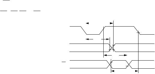
NOTE
1Applies after power-up sequence is complete. Internal phase lock loop requires no more than 2000 CLKIN cycles assuming stable CLKIN (not including crystal oscillator start-up time).
tCKI
tCKIH
CLKIN
tCKIL
tCKOH
tCKH
CLKOUT
tCKL
Figure 8. Clock Signals
REV. A |
–19– |
ADSP-2171/ADSP-2172/ADSP-2173
ADSP-2171/ADSP-2172
Parameter |
|
|
Min |
Max |
Unit |
|
|
|
|
|
|
Interrupts and Flags |
|
|
|
||
Timing Requirement: |
|
|
|
||
tIFS |
|
or FI Setup before CLKOUT Low1, 2, 3 |
0.25tCK + 15 |
|
ns |
IRQx |
|
||||
tIFH |
IRQx |
or FI Hold after CLKOUT High1, 2, 3 |
0.25tCK |
|
ns |
Switching Characteristic: |
|
|
|
||
tFOH |
Flag Output Hold after CLKOUT Low4 |
0.5tCK – 7 |
|
ns |
|
tFOD |
Flag Output Delay from CLKOUT Low4 |
|
0.5tCK + 5 |
ns |
|
NOTES
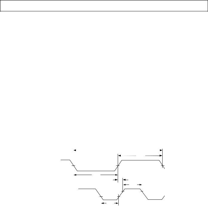
1If IRQx and FI inputs meet tIFS and tIFH setup/hold requirements, they will be recognized during the current clock cycle; otherwise the signals will be recognized on the following cycle. (Refer to “Interrupt Controller Operation” in the Program Control chapter of the User’s Manual for further information on interrupt servicing.) 2Edge-sensitive interrupts require pulse widths greater than 10 ns; level-sensitive interrupts must be held low until serviced.
3IRQx = IRQ0, IRQ1, and IRQ2.
4Flag Output = FL0, FL1, FL2, and FO.
tFOD
CLKOUT
tFOH
FLAG
OUTPUTS
tIFH
IRQx
FI
tIFS
Figure 9. Interrupts and Flags
–20– |
REV. A |