

ADSP-2171/ADSP-2172/ADSP-2173
ADSP-2171/ADSP-2172
Parameter |
|
|
|
|
|
|
|
|
|
|
|
|
|
|
|
|
|
|
|
|
|
|
|
|
|
|
|
|
|
|
|
|
|
|
|
|
|
|
Min |
Max |
Unit |
|
|
|
|
|
|
|
|
|
|
|
|
|
|
|
|
|
|
|
|
|
|
|
|
|
|
|
|
|
|
|
|
|
|
|
|
|
|
|
|
|
|
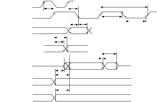
Bus Request/Grant |
|
|
|
||||||||||||||||||||||||||||||||||||||
Timing Requirement: |
|
|
|
||||||||||||||||||||||||||||||||||||||
tBH |
|
|
|
|
Hold after CLKOUT High1 |
0.25tCK + 2 |
|
ns |
|||||||||||||||||||||||||||||||||
BR |
|
||||||||||||||||||||||||||||||||||||||||
tBS |
BR |
|
|
|
Setup before CLKOUT Low1 |
0.25tCK + 17 |
|
ns |
|||||||||||||||||||||||||||||||||
Switching Characteristic: |
|
|
|
||||||||||||||||||||||||||||||||||||||
tSD |
CLKOUT High to |
|
|
|
|
|
|
|
, |
|
|
|
|
|
, |
|
|
, |
|
0.25tCK + 16 |
ns |
||||||||||||||||||||
DMS |
PMS |
BMS |
|
||||||||||||||||||||||||||||||||||||||
|
RD |
, |
WR |
Disable |
|
|
|
||||||||||||||||||||||||||||||||||
tSDB |
DMS |
, |
PMS |
, |
BMS |
|
, |
RD |
, |
|
WR |
|
|
|
|
|
|
||||||||||||||||||||||||
|
Disable to |
BG |
|
Low |
0 |
|
ns |
||||||||||||||||||||||||||||||||||
tSE |
BG |
|
High to |
DMS |
, |
PMS |
, |
BMS |
, |
|
|
|
|
||||||||||||||||||||||||||||
|
RD |
, |
WR |
Enable |
0 |
|
ns |
||||||||||||||||||||||||||||||||||
tSEC |
DMS |
, |
PMS |
, |
BMS |
, |
RD |
, |
WR |
|
|
|
|
|
|||||||||||||||||||||||||||
|
Enable to CLKOUT High |
0.25tCK – 7 |
|
ns |
|||||||||||||||||||||||||||||||||||||
tSDBH |
DMS |
, |
PMS |
, |
BMS |
, |
RD |
, |
WR |
|
|
|
|
|
|||||||||||||||||||||||||||
|
Disable to |
BGH |
Low2 |
0 |
|
ns |
|||||||||||||||||||||||||||||||||||
tSEH |
BGH |
High to |
DMS |
, |
PMS |
, |
BMS |
, |
|
|
|
||||||||||||||||||||||||||||||
|
RD |
, |
WR |
Enable2 |
0 |
|
ns |
||||||||||||||||||||||||||||||||||
NOTES
1BR is an asynchronous signal. If BR meets the setup/hold requirements, it will be recognized during the current clock cycle; otherwise the signal will be recognized on the following cycle. Refer to the ADSP-2100 Family User’s Manual for BR/BG cycle relationships.
2BGH is asserted when the bus is granted and the processor requires control of the bus to continue.
tBH
CLKOUT
BR
|
|
tBS |
CLKOUT |
|
|
PMS, DMS |
|
|
BMS, RD |
tSD |
tSEC |
WR |
||
BG |
|
tSDB |
|
|
tSE |
BGH |
|
tSDBH |
tSEH
Figure 10. Bus Request–Bus Grant
REV. A |
–21– |

ADSP-2171/ADSP-2172/ADSP-2173
ADSP-2171/ADSP-2172
Parameter |
|
|
|
|
|
|
|
|
|
|
|
|
|
|
|
|
|
|
|
|
|
|
|
|
|
Min |
Max |
Unit |
|
|
|
|
|
|
|
|
|
|
|
|
|
|
|
|
|
|
|
|
|
|
|
|
|
|
|
|
|
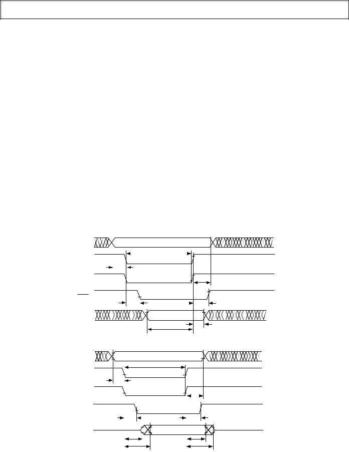
Memory Read |
|
|
|
|
|
|
|
|
|
|
|
|
|
|
|
|
|
|
|
|
|
|
|
|
|
|
|
|
Timing Requirement: |
|
|
|
|||||||||||||||||||||||||
tRDD |
|
Low to Data Valid |
|
0.5tCK – 9 + w |
ns |
|||||||||||||||||||||||
RD |
|
|||||||||||||||||||||||||||
tAA |
A0–A13, |
PMS |
, |
DMS |
, |
BMS |
|
to Data Valid |
|
0.75tCK – 10.5 + w |
ns |
|||||||||||||||||
tRDH |
Data Hold from |
RD |
High |
0 |
|
ns |
||||||||||||||||||||||
Switching Characteristic: |
|
|
|
|||||||||||||||||||||||||
tRP |
|
Pulse Width |
0.5tCK – 5 + w |
|
ns |
|||||||||||||||||||||||
RD |
|
|||||||||||||||||||||||||||
tCRD |
CLKOUT High to |
RD |
|
Low |
0.25tCK – 5 |
0.25tCK + 7 |
ns |
|||||||||||||||||||||
tASR |
A0–A13, |
PMS |
, |
DMS |
, |
BMS |
|
Setup before |
RD |
Low |
0.25tCK – 6 |
|
ns |
|||||||||||||||
tRDA |
A0–A13, |
PMS |
, |
DMS |
, |
BMS |
Hold after |
RD |
Deasserted |
0.25tCK – 3 |
|
ns |
||||||||||||||||
tRWR |
RD |
High to |
RD |
or |
WR |
Low |
0.5tCK – 5 |
|
ns |
|||||||||||||||||||
w = wait states x tCK.
CLKOUT
A0–A13
DMS, PMS
BMS
|
|
|
|
|
|
|
|
|
|
|
|
tRDA |
|
|
|
|
|
|
|
|
|
|
|
|
|
|
|
|
|
|
|
RD |
|
|
|
|
|||||||||||
|
|
|
|
|
|
|
|
|
|
|
|
|
|
||
|
|
|
tASR |
|
|
|
|
||||||||
|
|
|
|
|
|
|
|
|
tRP |
|
|
|
|
|
|
|
|
|
t |
||||||||||||
|
|
|
|
|
|
|
|
|
|
|
|
||||
|
|
tCRD |
|
|
|
|
|
|
|
||||||
|
|
|
|
|
|
|
|
|
|
RWR |
|||||
|
|
|
|
|
|||||||||||
|
|
|
|
|
|||||||||||
|
|
|
|
|
|
|
|
|
|
|
|||||
D |
|
|
|
|
|||||||||||
|
|
|
|
|
|
|
|
|
|
|
|
|
|||
|
|
|
|
|
|
|
|
tRDD |
|
||||||
|
|
|
|
|
|
|
|
|
|
|
tRDH |
||||
|
|
|
|
tAA |
|
|
|
|
|
|
|
||||
|
|
|
|
|
|
|
|
|
|
|
|
|
|||
WR
Figure 11. Memory Read
–22– |
REV. A |

ADSP-2171/ADSP-2172/ADSP-2173
ADSP-2171/ADSP-2172
Parameter |
|
|
|
|
|
|
|
|
|
|
|
|
|
|
|
|
|
|
|
|
|
|
|
|
|
|
|
|
Min |
Max |
Unit |
|
|
|
|
|
|
|
|
|
|
|
|
|
|
|
|
|
|
|
|
|
|
|
|
|
|
|
|
|
|
|
|
Memory Write |
|
|
|
|
|
|
|
|
|
|
|
|
|
|
|
|
|
|
|
|
|
|
|
|
|
|
|
|
|
|
|
Switching Characteristic: |
|
|
|
||||||||||||||||||||||||||||
tDW |
Data Setup before |
|
|
|
|
|
|
|
High |
0.5 tCK – 7 + w |
|
ns |
|||||||||||||||||||
WR |
|
||||||||||||||||||||||||||||||
tDH |
Data Hold after |
WR |
|
High |
0.25tCK – 2 |
|
ns |
||||||||||||||||||||||||
tWP |
WR |
Pulse Width |
0.5tCK – 5 + w |
|
ns |
||||||||||||||||||||||||||
tWDE |
WR |
Low to Data Enabled |
0 |
|
ns |
||||||||||||||||||||||||||
tASW |
A0–A13, |
DMS |
, |
|
PMS |
|
Setup before |
WR |
Low |
0.25tCK – 6 |
|
ns |
|||||||||||||||||||
tDDR |
Data Disable before |
WR |
or |
RD |
Low |
0.25tCK – 7 |
|
ns |
|||||||||||||||||||||||
tCWR |
CLKOUT High to |
WR |
|
Low |
0.25tCK – 5 |
0.25 tCK + 7 |
ns |
||||||||||||||||||||||||
tAW |
A0–A13, |
DMS |
|
, |
PMS |
, Setup before |
WR |
Deasserted |
0.75tCK – 9 + w |
|
ns |
||||||||||||||||||||
tWRA |
A0–A13, |
DMS |
|
, |
PMS |
Hold after |
WR |
Deasserted |
0.25tCK – 3 |
|
ns |
||||||||||||||||||||
tWWR |
WR |
High to |
RD |
or |
WR |
Low |
0.5tCK – 5 |
|
ns |
||||||||||||||||||||||
w = wait states x tCK.
CLKOUT
A0–A13
DMS, PMS
 tWRA
tWRA 
WR
tCWR
tAS W |
|
|
|
tWP |
|
tWWR |
|
|
|
tAW |
|
|
tDH |
|
tDD R |
|
|
|
|
|
|
D


 tDW tWDE
RD
Figure 12. Memory Write
REV. A |
–23– |
ADSP-2171/ADSP-2172/ADSP-2173
ADSP-2171/ADSP-2172
Parameter |
|
|
|
|
|
Min |
|
|
Max |
Unit |
|||
|
|
|
|
|
|
|
|
|
|
|
|
|
|
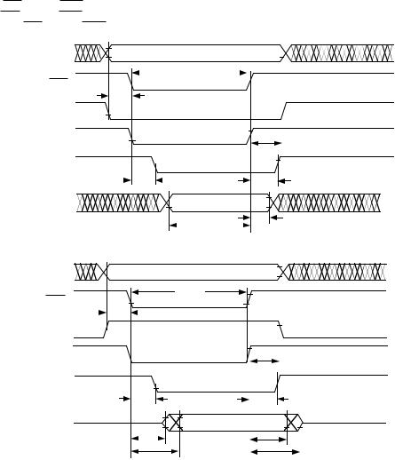
Serial Ports |
|
|
|
|
|
|
|
|
|
|
|
|
|
Timing Requirement: |
|
|
|
|
|
|
|
|
|
|
|
|
|
tSCK |
SCLK Period |
|
|
|
|
50 |
|
|
|
|
|
|
ns |
tSCS |
DR/TFS/RFS Setup before SCLK Low |
|
4 |
|
|
|
|
|
|
ns |
|||
tSCH |
DR/TFS/RFS Hold after SCLK Low |
|
7 |
|
|
|
|
|
|
ns |
|||
tSCP |
SCLKIN Width |
|
|
|
|
20 |
|
|
|
|
|
|
ns |
Switching Characteristic: |
|
|
|
|
|
|
|
|
|
|
|
|
|
tCC |
CLKOUT High to SCLKOUT |
|
0.25tCK |
|
|
0.25tCK + 10 |
ns |
||||||
tSCDE |
SCLK High to DT Enable |
|
|
|
|
0 |
|
|
|
|
|
|
ns |
tSCDV |
SCLK High to DT Valid |
|
|
|
|
|
|
|
15 |
ns |
|||
tRH |
TFS/RFSOUT Hold after SCLK High |
|
0 |
|
|
|
|
|
|
ns |
|||
tRD |
TFS/RFSOUT Delay from SCLK High |
|
|
|
|
15 |
ns |
||||||
tSCDH |
DT Hold after SCLK High |
|
|
|
|
0 |
|
|
|
|
|
|
ns |
tTDE |
TFS(Alt) to DT Enable |
|
|
|
|
0 |
|
|
|
|
|
|
ns |
tTDV |
TFS(Alt) to DT Valid |
|
|
|
|
|
|
|
15 |
ns |
|||
tSCDD |
SCLK High to DT Disable |
|
|
|
|
|
|
|
15 |
ns |
|||
tRDV |
RFS (Multichannel, Frame Delay Zero) to DT Valid |
|
|
|
15 |
ns |
|||||||
|
CLKOUT |
tCC |
tCC |
|
|
|
|
|
|
|
|
||
|
|
|
|
|
|
|
|
|
|
||||
|
|
|
|
|
tSCK |
|
|
|
|
||||
|
|
|
|
|
|
|
|
|
|
|
|
|
|
|
SCLK |
|
|
|
|
|
|
|
|
|
|
|
|
|
|
|
|
|
|
tSCP |
|
|
|
|
|
|
|
|
|
|
|
|
|
|
|
|
|
|
|
|
|
|
|
|
|
|
tSCS tSCH |
|
|
|
|
|
|
|
|
|
|
|
|
|
|
|
|
|
|
tSCP |
|
||
|
DR |
|
|
|
|
|
|
|
|
|
|
|
|
|
RFSIN |
|
|
|
|
|
|
|
|
|
|
|
|
|
TFSIN |
|
|
|
|
|
|
|
|
|
|
|
|
|
|
|
tRD |
|
|
|
|
|
|
|
|
|
|
|
|
|
tRH |
|
|
|
|
|
|
|
|
|
|
|
RFSOUT |
|
|
|
|
|
|
|
|
|
|
|
|
|
TFSOUT |
|
|
|
|
tSCDD |
|
|
|
|
|
||
tSCDV 

tSCDE 
 tSCDH
tSCDH 
DT
tTDE tTDV
TFS
ALTERNATE
FRAME MODE
tRDV
RFS
MULTICHANNEL MODE, FRAME DELAY 0 (MFD = 0)
Figure 13. Serial Ports
–24– |
REV. A |
ADSP-2171/ADSP-2172/ADSP-2173
ADSP-2171/ADSP-2172
Parameter |
|
|
|
|
|
|
|
|
|
|
|
|
|
|
|
|
|
|
|
|
|
|
|
Min |
Max |
Unit |
|||||||
|
|
|
|
|
|
|
|
|
|
|
|
|
|
|
|
|
|
|
|
|
|
|
|
|
|
|
|
|
|
|
|
|
|
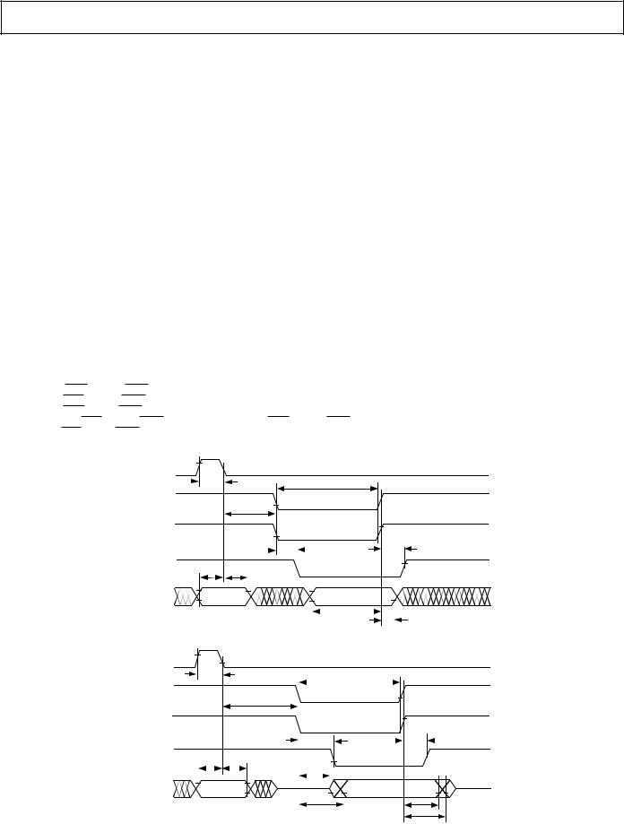
Host Interface Port |
|
|
|
|
|
|
|
|
|
|
|||||||||||||||||||||||
Separate Data and Address (HMD1 = 0) |
|
|
|
|
|
|
|
|
|
|
|||||||||||||||||||||||
Read Strobe and Write Strobe (HMD0 = 0) |
|
|
|
|
|
|
|
|
|
|
|||||||||||||||||||||||
Timing Requirement: |
|
|
|
|
|
|
|
|
|
|
|||||||||||||||||||||||
tHSU |
HA2–0 Setup before Start of Write or Read1, 2 |
|
5 |
|
ns |
||||||||||||||||||||||||||||
tHDSU |
Data Setup before End of Write3 |
|
|
|
|
|
|
|
5 |
|
ns |
||||||||||||||||||||||
tHWDH |
Data Hold after End of Write3 |
|
|
|
|
|
|
|
3 |
|
ns |
||||||||||||||||||||||
tHH |
HA2–0 Hold after End of Write or Read3, 4 |
|
3 |
|
ns |
||||||||||||||||||||||||||||
tHRWP |
Read or Write Pulse Width5 |
|
|
|
|
|
|
|
20 |
|
ns |
||||||||||||||||||||||
Switching Characteristic: |
|
|
|
|
|
|
|
|
|
|
|||||||||||||||||||||||
tHSHK |
|
|
|
|
|
|
Low after Start of Write or Read1, 2 |
|
0 |
15 |
ns |
||||||||||||||||||||||
HACK |
|||||||||||||||||||||||||||||||||
tHKH |
HACK |
|
Hold after End of Write or Read3, 4 |
|
0 |
15 |
ns |
||||||||||||||||||||||||||
tHDE |
Data Enabled after Start of Read2 |
|
|
|
|
|
|
|
0 |
|
ns |
||||||||||||||||||||||
tHDD |
Data Valid after Start of Read2 |
|
|
|
|
|
|
|
|
18 |
ns |
||||||||||||||||||||||
tHRDH |
Data Hold after End of Read4 |
|
|
|
|
|
|
|
0 |
|
ns |
||||||||||||||||||||||
tHRDD |
Data Disabled after End of Read4 |
|
|
|
|
|
|
|
|
7 |
ns |
||||||||||||||||||||||
NOTES |
|
|
|
|
|
|
|
|
|
|
|
|
|
|
|
|
|
|
|
|
|
|
|
|
|
|
|||||||
1Start of Write = |
HWR |
Low and |
HSEL |
Low. |
|
|
|
|
|
|
|
|
|
|
|||||||||||||||||||
2Start of Read = |
HRD |
|
Low and |
HSEL |
Low. |
|
|
|
|
|
|
|
|
|
|
||||||||||||||||||
3End of Write = |
HWR |
High or |
HSEL |
High. |
|
|
|
|
|
|
|
|
|
|
|||||||||||||||||||
4End of Read = |
HRD |
|
High or |
HSEL |
|
High. |
|
|
|
|
|
|
|
|
|
|
|||||||||||||||||
5Read Pulse Width = |
HRD |
Low and |
HSEL |
Low, Write Pulse Width = |
HWR |
Low and |
HSEL |
Low. |
|
|
|
||||||||||||||||||||||
|
|
|
|
|
|
|
|
|
|
|
|
|
|
|
|
HA2–0 |
ADDRESS |
|
|
|
|||||||||||||
|
|
|
|
|
|
|
|
|
|
|
|
|
|
|
|
|
|
|
|
|
|
|
|
|
|
|
|
|
|
|
|||
|
|
|
|
|
|
|
|
|
|
|
|
|
|
|
|
|
|
|
|
|
|
|
|
|
tHRWP |
|
|
|
|||||
|
|
|
|
|
|
|
|
|
|
|
|
|
|
|
|
|
HSEL |
|
|
|
|||||||||||||
|
|
|
|
|
|
|
|
|
|
|
|
|
|
|
|
|
|
|
|
|
|
|
|
|
|
|
|||||||
|
|
|
|
|
|
|
|
|
|
|
|
|
|
|
|
|
|
|
|
|
|
|
|
|
|
|
|||||||
Host Write Cycle
tHSU
HWR |
tHH |
HACK
tHSHK |
|
tHKH |
Host Read Cycle
HD15–0 |
|
|
DATA |
|
||||||
|
|
|
|
|
|
|
|
|
|
tHWDH |
|
|
|
|
|
|
|
|
tHDSU |
|
|
|
|
|
|
|
|
|
|
|
|
|
HA2–0 |
|
ADDRESS |
|
|||||||
|
|
|
|
|
|
|
|
|
|
|
|
|
|
|
|
|
|
tHRWP |
|
||
|
|
HSEL |
|
|||||||
|
|
|
|
|
|
|
||||
|
|
tHSU |
|
|||||||
|
|
|
|
|
|
|
||||
|
|
|
|
|
|
|
|
|
|
tHH |
|
|
|
HRD |
|
|
|
|
|||
|
|
|
|
|
|
|
|
|||
|
HACK |
|
|
|
|
|
||||
|
|
|
|
|
|
|
tHSHK |
tHKH |
||
HD15–0 |
DATA |
|
tHDE |
t |
HRDH |
|
|
|
tHDD |
tHRDD |
|
Figure 14. Host Interface Port (HMD1 = 0, HMD0 = 0)
REV. A |
–25– |
ADSP-2171/ADSP-2172/ADSP-2173
ADSP-2171/ADSP-2172
Parameter |
|
|
Min |
Max |
Unit |
|
|
|
|
|
|
Host Interface Port |
|
|
|
||
Separate Data and Address (HMD1 = 0) |
|
|
|
||
Read Strobe and Write Strobe (HMD0 = 1) |
|
|
|
||
Timing Requirement: |
|
|
|
||
tHSU |
HA2–0, HRW Setup before Start of Write or Read1 |
5 |
|
ns |
|
tHDSU |
Data Setup before End of Write2 |
5 |
|
ns |
|
tHWDH |
Data Hold after End of Write2 |
3 |
|
ns |
|
tHH |
HA2–0, HRW Hold after End of Write or Read2 |
3 |
|
ns |
|
tHRWP |
Read or Write Pulse Width3 |
20 |
|
ns |
|
Switching Characteristic: |
|
|
|
||
tHSHK |
|
Low after Start of Write or Read1 |
0 |
15 |
ns |
HACK |
|||||
tHKH |
HACK |
Hold after End of Write or Read2 |
0 |
15 |
ns |
tHDE |
Data Enabled after Start of Read1 |
0 |
|
ns |
|
tHDD |
Data Valid after Start of Read1 |
|
18 |
ns |
|
tHRDH |
Data Hold after End of Read2 |
0 |
|
ns |
|
tHRDD |
Data Disabled after End of Read2 |
|
7 |
ns |
|
NOTES
1Start of Write or Read = HDS Low and HSEL Low. 2End of Write or Read = HDS High and HSEL High. 3Read or Write Pulse Width = HDS Low and HSEL Low.
Host Write Cycle
Host Read Cycle
HA2–0 |
ADDRESS |
tHRWP
HSEL
tHSU
HRW
|
|
HDS |
|
|
|
|
tHH |
|
|
|
|
|
|
|
|
|
|
HACK |
|
|
|
|
||||
|
|
|
|
|
tHSHK |
tHKH |
||
HD15–0 |
|
DATA |
|
|||||
|
|
|
|
|
|
|
|
tHWDH |
|
|
|
|
|
|
tHDSU |
|
|
|
|
|
|
|
|
|
|
|
HA2–0 |
ADDRESS |
|
||||||
tHRWP
HSEL
tHSU
HRW
|
|
HDS |
|
|
|
|
|
|
tHH |
|
|
|
|
|
|
|
|
||
HACK |
|
|
|
|
|
||||
|
|
|
|
tHSHK |
|
|
|
|
tHKH |
HD15–0 |
DATA |
||||||||
|
|
|
|
tHDE |
|
|
|
|
|
|
|
|
|
|
tHRDH |
||||
|
|
|
|
tHDD |
|
|
|
|
|
|
|
|
|
|
t |
HRDD |
|
||
|
|
|
|
|
|
|
|
||
Figure 15. Host Interface Port (HMD1 = 0, HMD0 = 1)
–26– |
REV. A |
ADSP-2171/ADSP-2172/ADSP-2173
ADSP-2171/ADSP-2172
Parameter |
|
|
Min |
Max |
Unit |
|
|
|
|
|
|
Host Interface Port |
|
|
|
||
Multiplexed Data and Address (HMD1 = 1) |
|
|
|
||
Read Strobe and Write Strobe (HMD0 = 0) |
|
|
|
||
Timing Requirement: |
|
|
|
||
tHALP |
ALE Pulse Width |
10 |
|
ns |
|
tHASU |
HAD15–0 Address Setup, before ALE Low |
5 |
|
ns |
|
tHAH |
HAD15–0 Address Hold after ALE Low |
2 |
|
ns |
|
tHALS |
Start of Write or Read after ALE Low1, 2 |
10 |
|
ns |
|
tHDSU |
HAD15–0 Data Setup before End of Write3 |
5 |
|
ns |
|
tHWDH |
HAD15–0 Data Hold after End of Write3 |
3 |
|
ns |
|
tHRWP |
Read or Write Pulse Width4 |
20 |
|
ns |
|
Switching Characteristic: |
|
|
|
||
tHSHK |
|
Low after Start of Write or Read1, 2 |
0 |
15 |
ns |
HACK |
|||||
tHKH |
HACK |
Hold after End of Write or Read3, 5 |
0 |
15 |
ns |
tHDE |
HAD15–0 Data Enabled after Start of Read2 |
0 |
|
ns |
|
tHDD |
HAD15–0 Data Valid after Start of Read2 |
|
18 |
ns |
|
tHRDH |
HAD15–0 Data Hold after End of Read |
0 |
|
ns |
|
tHRDD |
HAD15–0 Data Disabled after End of Read5 |
|
7 |
ns |
|
NOTES
1Start of Write = HWR Low and HSEL Low.
2Start of Read = HRD Low and HSEL Low. 3End of Write = HWR High or HSEL High.
4Read Pulse Width = HRD Low and HSEL Low, Write Pulse Width = HWR Low and HSEL Low. 5End of Read = HRD High or HSEL High.
Host Write Cycle
Host Read Cycle
ALE
|
|
|
|
|
|
tHALP |
|
|
|
||
|
|
|
|
|
|
tHRWP |
|
|
|||
|
|
|
|
|
|
|
|
|
|
|
|
|
HSEL |
|
|
|
|
|
|
||||
|
|
|
|
tHALS |
|
|
|
|
|||
|
|
|
|
|
|
|
|
|
|
|
|
|
|
|
|
|
|
|
|
|
|
|
|
|
HWR |
|
|
|
|
|
|
||||
|
|
|
|
|
|
|
|
|
tHSHK |
|
tHKH |
|
|
|
|
|
|
tHASU tHAH |
|
|
|
||
HACK |
|
|
|
||||||||
HD15–0 |
ADDRESS |
|
|
DATA |
|||||||
|
|
|
|
|
|
|
|
|
|
tHDSU |
|
tHWDH
ALE
|
|
|
|
|
|
tHALP |
|
|
|
|
|
|
|
|
|
|
|
|
|
|
|
|
|
|
tHRWP |
|
|
|
|
|
|
|
|
|
|
|
|
|
|
|
|
|
|
|
|
|
|
|
|
|
|
|
|
|
|
|
HSEL |
|
|
|
|
|
|
|
|
||||
|
|
|
|
|
|
|
|
|
|
|
|
|
|
|
|
|
|
|
|
|
|
tHALS |
|
|
|||
|
|
|
|
|
|
|
|
|
|
|
|
|
|
|
HRD |
|
|
|
|
|
|
|
|
||||
|
|
|
|
|
|
|
|
|
tHSHK |
|
tHKH |
||
|
|
|
|
|
|
tHASU |
tHAH |
|
|
|
|
|
|
HACK |
|
tHDE |
|
|
|||||||||
|
|
|
|
|
|
|
|
|
|
|
|||
HAD15–0 |
ADDRESS |
|
|
|
|
|
DATA |
||||||
|
|
|
|
|
|
|
|
|
|
|
|
|
tHRDH |
|
|
|
|
|
|
|
|
|
|
tHDD |
|
||
|
|
|
|
|
|
|
|
|
|
|
|
|
tHRDD |
Figure 16. Host Interface Port (HMD1 = 1, HMD0 = 0)
REV. A |
–27– |

ADSP-2171/ADSP-2172/ADSP-2173
ADSP-2171/ADSP-2172
Parameter |
|
|
Min |
Max |
Unit |
|
|
|
|
|
|
Host Interface Port |
|
|
|
||
Multiplexed Data and Address (HMD1 = 1) |
|
|
|
||
Read Strobe and Write Strobe (HMD0 = 1) |
|
|
|
||
Timing Requirement: |
|
|
|
||
tHALP |
ALE Pulse Width |
10 |
|
ns |
|
tHASU |
HAD15–0 Address Setup before ALE Low |
5 |
|
ns |
|
tHAH |
HAD15–0 Address Hold after ALE Low |
2 |
|
ns |
|
tHALS |
Start of Write or Read after ALE Low1 |
10 |
|
ns |
|
tHSU |
HRW Setup before Start of Write or Read1 |
5 |
|
ns |
|
tHDSU |
HAD15–0 Data Setup before End of Write2 |
5 |
|
ns |
|
tHWDH |
HAD15–0 Data Hold after End of Write2 |
3 |
|
ns |
|
tHH |
HRW Hold after End of Write or Read2 |
3 |
|
ns |
|
tHRWP |
Read or Write Pulse Width3 |
20 |
|
ns |
|
Switching Characteristic: |
|
|
|
||
tHSHK |
|
Low after Start of Write or Read1 |
0 |
15 |
ns |
HACK |
|||||
tHKH |
HACK |
Hold after End of Write or Read2 |
0 |
15 |
ns |
tHDE |
HAD15–0 Data Enabled after Start of Read1 |
0 |
|
ns |
|
tHDD |
HAD15–0 Data Valid after Start of Read1 |
|
18 |
ns |
|
tHRDH |
HAD15–0 Data Hold after End of Read2 |
0 |
|
ns |
|
tHRDD |
HAD15–0 Data Disabled after End of Read2 |
|
7 |
ns |
|
NOTES
1Start of Write or Read = HDS Low and HSEL Low. 2End of Write or Read = HDS High and HSEL High. 3Read or Write Pulse Width = HDS Low and HSEL Low.
Host Write Cycle
Host Read Cycle
ALE
tHALP
|
|
|
|
|
|
|
|
|
|
|
|
|
|
|
|
|
|
|
|
tHRWP |
|
|
|
|
|
|
|
|
|
HSEL |
|
|
|
|
|
|
|
|
|
|
|
|
|
|
|
|
|
|
|
|
tHH |
|
|
||
|
|
|
|
|
|
|
|
|
|
|
|
|
|
|
|
|
|
|
|
|
|
|
|
|
|
|
|
|
|
HRW |
|
|
|
tHALS |
|
|
|
|
|
|
|
|
|
|
|||||||||||
|
|
|
|
|
|
|
|
|
|
|
|
|
|
|
|
|
|
|
|
|
|||||||
|
|
|
|
|
|
|
|
|
|
|
|
|
|
|
|
|
|
|
|
|
|
|
|||||
|
|
|
|
|
|
|
|
|
|
|
|
|
|
|
|
|
|
|
|
|
|
|
|
|
|
|
|
|
|
|
|
|
|
|
|
|
|
|
|
|
|
|
|
tHSU |
|
|
|
|
|
|
|||||
|
|
|
|
|
|
|
|
|
|
|
|
|
|
|
|
|
|
|
|
|
|
|
|
|
|
|
|
|
|
|
HDS |
|
|
|
|
|
|
|
|
|
|
|
|
|
|
|
|
|
|
|
|
|
|||
|
|
|
|
|
|
|
|
|
|
|
|
|
|
|
|
|
|
|
|
tHSHK |
|
|
tHKH |
||||
|
|
|
|
|
|
|
tHASU |
tHAH |
|
|
|
|
|
|
|
|
|
|
|
|
|
|
|
|
|||
|
HACK |
|
|
|
|
|
|
|
|
|
|
|
|
|
|
|
|
||||||||||
HD15–0 |
ADDRESS |
|
|
|
|
|
|
|
|
|
|
DATA |
|||||||||||||||
|
|
|
|
|
|
|
|
|
|
|
|
|
|
|
|
|
|
|
|
tHDSU |
|
|
|
|
|
||
|
|
|
|
|
|
|
|
|
|
|
|
|
|
|
|
|
|
|
|
tHWDH |
|||||||
|
|
|
|
|
|
|
|
|
|
|
|
|
|
|
|
|
|
|
|
|
|
|
|||||
|
|
|
ALE |
|
|
|
|
|
|
|
|
|
|
|
|
|
|
|
|
|
|
|
|
|
|||
|
|
|
|
|
|
|
tHALP |
|
|
|
|
|
|
|
|
|
|
|
|
|
|
|
|
|
|
|
|
|
|
|
|
|
|
|
|
tHALS |
|
|
|
|
|
|
|
|
|
tHRWP |
|
|
|
|
|
|
|||
|
|
|
|
|
|
|
|
|
|
|
|
|
|
|
|
|
|
|
|
|
|
|
|
|
|
|
|
|
|
HSEL |
|
|
|
|
|
|
|
|
|
|
|
|
|
|
|
|
|
|
|
|
|
||||
|
|
|
|
|
|
|
|
|
|
|
|
|
|
|
|
|
|
|
|
|
|
|
|||||
|
|
HRW |
|
|
|
|
|
|
|
|
|
|
|
|
|
|
|
|
|
|
tHH |
||||||
|
|
|
|
|
|
|
|
|
|
|
|
|
|
|
|
|
|
|
|
|
|
|
|||||
|
|
|
|
|
|
|
|
|
|
|
|
|
tHSU |
|
|
|
|
|
|
|
|
|
|||||
|
|
|
|
|
|
|
|
|
|
|
|
|
|
|
|
|
|
|
|
|
|
|
|
|
|
|
|
|
|
|
HDS |
|
|
|
|
|
|
|
|
|
|
|
|
|
|
|
|
|
|
|
|
|
|||
|
|
|
|
|
|
|
|
|
|
|
|
|
|
|
|
|
|
|
|
|
|
|
|
tHKH |
|||
|
|
|
|
|
|
|
|
|
|
|
|
|
|
|
|
|
|
|
|
tHSHK |
|
|
|||||
|
|
|
|
|
|
|
tHASU |
tHAH |
|
|
|
|
|
|
|
|
|
|
|
|
|
|
|
|
|||
|
|
HACK |
|
|
|
|
|
|
|
|
|
|
|
|
|
|
|
|
|||||||||
|
|
|
|
|
|
|
|
|
|
|
|
|
|
|
tHDE |
|
|
|
|
|
|
|
|||||
HD15–0 |
ADDRESS |
|
|
|
|
|
|
|
|
|
|
DATA |
|||||||||||||||
|
|
|
|
|
|
|
|
|
|
|
|
|
|
|
tHDD |
tHRDH |
|||||||||||
tHRDD
Figure 17. Host Interface Port (HMD1 = 1, HMD0 = 1)
–28– |
REV. A |
ADSP-2171/ADSP-2172/ADSP-2173
ADSP-2171/ADSP-2172
ENVIRONMENTAL CONDITIONS
Ambient Temperature Rating:
TAMB = TCASE – (PD × θCA)
TCASE = Case Temperature in °C PD = Power Dissipation in W
θCA = Thermal Resistance (Case-to-Ambient)
θJA = Thermal Resistance (Junction-to-Ambient)
θJC = Thermal Resistance (Junction-to-Case)
Package |
θJA |
θJC |
θCA |
|
|
|
|
TQFP |
50°C/W |
2°C/W |
48°C/W |
PQFP |
41°C/W |
10°C/W |
31°C/W |
|
|
|
|
POWER DISSIPATION
To determine total power dissipation in a specific application, the following equation should be applied for each output:
C × VDD2 × f
C = load capacitance, f = output switching frequency.
Example:
In an application where external data memory is used and no other outputs are active, power dissipation is calculated as follows:
Assumptions:
•External data memory is accessed every cycle with 50% of the address pins switching.
•External data memory writes occur every other cycle with 50% of the data pins switching.
•Each address and data pin has a 10 pF total load at the pin.
•The application operates at VDD = 5.0 V and tCK = 30 ns.
Total Power Dissipation = PINT + (C × VDD2 × f )
PINT = internal power dissipation from Power vs. Frequency graph (Figure 18).
(C × VDD2 × f ) is calculated for each output:
|
|
|
|
|
|
# of |
× C |
× VDD2 |
× f |
|
|
|
|
|
|
|
|
|
|
Pins |
|
|
|
||||
Address, |
|
|
|
|
8 |
× 10 pF |
× 52 |
V |
× 33.3 MHz |
= |
66.6 mW |
||
DMS |
|||||||||||||
Data Output, |
|
|
9 |
× 10 pF |
× 52 |
V |
× 16.67 MHz |
= |
37.5 mW |
||||
WR |
|||||||||||||
|
|
1 |
× 10 pF |
× 52 |
V |
× 16.67 MHz |
= |
4.2 mW |
|||||
RD |
|||||||||||||
CLKOUT |
1 |
× 10 pF |
× 52 |
V |
× 33.3 MHz |
= |
8.3 mW |
||||||
|
|
|
|
|
|
|
|
|
|
|
|
116.6 mW |
|
|
|
|
|
|
|
|
|
|
|
|
|
|
|
Total power dissipation for this example is PINT + 116.6 mW.
POWER, INTERNAL 1
|
400 |
|
|
|
|
|
|
|
|
382mW |
|
|
|
375 |
|
|
|
|
|
|
|
|
|
||
|
|
|
|
|
|
|
|
|
|
|
|
|
|
350 |
|
|
|
|
|
|
|
|
|
|
|
|
325 |
|
|
|
|
|
|
|
|
301mW |
||
mW |
300 |
|
|
|
|
|
|
|
|
|||
|
|
VDD = 5.5V |
|
|
|
|
|
|
||||
|
|
|
|
|
|
|
|
|
||||
) – |
275 |
|
|
|
|
|
|
|
|
|||
|
|
|
|
|
|
|
|
|
|
|
||
INT |
250 |
|
|
|
|
|
|
|
|
|
|
|
(P |
|
|
|
|
VDD = 5.0V |
|
229mW |
|
||||
|
|
|
|
|
|
|
||||||
POWER |
225 |
186mW |
|
|
|
|
|
|
|
|
|
|
|
|
|
|
|
|
|
|
|
|
|||
200 |
|
|
|
|
VDD = 4.5V |
|
|
|
|
|||
|
175 |
148mW |
|
|
|
|
|
|
|
|
|
|
|
|
|
|
|
|
|
|
|
|
|
||
|
150 |
|
|
|
|
|
|
|
|
|
|
|
|
125 |
110mW |
|
|
|
|
|
|
|
|
|
|
|
|
13 |
15 |
17 |
19 |
21 |
23 |
25 |
27 |
29 |
31 |
33 |
|
|
|
|
|
|
1/ tCK – MHz |
|
|
|
|
||
POWER, IDLE 1, 2
|
85 |
|
|
|
|
|
|
|
|
82mW |
|
|
|
80 |
|
|
|
|
|
|
|
|
|
||
|
|
|
|
|
|
|
|
|
|
|
|
|
|
75 |
|
|
|
|
|
|
|
|
|
|
|
|
70 |
|
|
|
|
|
|
|
|
|
|
|
mW |
65 |
|
|
VDD = 5.5V |
|
|
64mW |
|
||||
) – |
60 |
|
|
|
|
|
|
|
|
|
|
|
|
|
|
|
|
|
|
|
|
|
|
|
|
IDLE |
|
|
|
|
|
|
|
|
|
|
|
|
(P |
55 |
48mW |
|
|
|
VDD = 5.0V |
|
|
|
|
||
POWER |
50 |
|
|
|
|
|
|
|
|
48mW |
|
|
45 |
|
|
|
|
|
VDD = 4.5V |
|
|
|
|||
40 |
|
|
|
|
|
|
|
|
||||
|
37mW |
|
|
|
|
|
|
|
|
|
|
|
|
|
|
|
|
|
|
|
|
|
|
|
|
|
35 |
|
|
|
|
|
|
|
|
|
|
|
|
30 |
26mW |
|
|
|
|
|
|
|
|
|
|
|
|
|
|
|
|
|
|
|
|
|
|
|
|
|
13 |
15 |
17 |
19 |
21 |
23 |
25 |
27 |
29 |
31 |
33 |
|
|
|
|
|
|
1/ tCK – MHz |
|
|
|
|
||
POWER, IDLE n MODES 3
|
72 |
|
|
|
|
|
|
|
|
82mW |
|
|
|
68 |
|
|
|
|
|
|
|
|
|
||
|
|
|
|
|
|
|
|
|
|
64mW |
||
|
|
|
|
|
|
|
|
|
|
|
||
|
64 |
|
|
|
|
|
|
|
|
|
|
IDLE; |
mW |
60 |
|
|
|
|
|
|
|
|
|
|
|
56 |
|
|
|
|
|
|
|
|
|
|
|
|
) – |
|
|
|
|
|
|
|
|
|
|
|
|
|
|
|
|
|
|
|
|
|
|
|
|
|
n |
|
|
|
|
|
|
|
|
|
|
|
|
|
52 |
|
|
|
|
|
|
|
|
|
|
|
IDLE |
|
|
|
|
|
|
|
|
|
|
|
|
(P |
48 |
|
|
|
|
|
|
|
|
|
|
|
POWER |
44 |
|
|
|
|
|
|
|
|
|
|
|
40 |
37mW |
|
|
|
|
|
|
|
|
|
|
|
36 |
|
|
|
|
|
|
|
|
|
|
|
|
|
|
|
|
|
|
|
|
|
|
|
|
|
|
32 |
|
|
|
|
|
|
|
|
|
31mW |
|
|
|
|
|
|
|
|
|
|
|
|
IDLE (16) |
|
|
28 |
23mW |
|
|
|
|
|
|
|
|
|
IDLE (128) |
|
24 |
|
|
|
|
|
|
|
|
28mW |
||
|
|
|
|
|
|
|
|
|
|
|
|
|
|
20 |
|
|
|
|
|
|
|
|
|
|
|
|
16 |
20mW |
|
|
|
|
|
|
|
|
|
|
|
|
|
|
|
|
|
|
|
|
|
|
|
|
|
13 |
15 |
17 |
19 |
21 |
23 |
25 |
27 |
29 |
31 |
33 |
|
|
|
|
|
|
1/ tCK – MHz |
|
|
|
|
||
VALID FOR ALL TEMPERATURE GRADES.
1POWER REFLECTS DEVICE OPERATING WITH NO OUTPUT LOADS.
2IDLE REFERS TO ADSP-2171 STATE OF OPERATION DURING EXECUTION OF IDLE INSTRUCTION. DEASSERTED PINS ARE
DRIVEN TO EITHER VDD OR GND. POWER REFLECTS DEVICE OPERATING WITH CLKOUT DISABLED.
3TYPICAL POWER DISSIPATION AT 5.0V VDD DURING EXECUTION OF IDLE N INSTRUCTION (CLOCK FREQUENCY REDUCTION).
POWER REFLECTS DEVICE OPERATING WITH CLKOUT DISABLED.
Figure 18. Power vs. Frequency
REV. A |
–29– |

ADSP-2171/ADSP-2172/ADSP-2173
ADSP-2171/ADSP-2172
CAPACITIVE LOADING
Figures 19 and 20 show the capacitive loading characteristics of the ADSP-2171/ADSP-2172.
|
28 |
|
|
|
|
|
|
|
|
24 |
|
|
|
|
|
|
|
– ns |
20 |
|
|
|
|
|
|
|
2.4V) |
|
|
|
|
|
|
|
|
|
|
|
|
|
|
|
|
|
16 |
|
|
VDD = 4.5V |
|
|
|
|
|
- |
|
|
|
|
|
|
|
|
(0.4V |
|
|
|
|
|
|
|
|
TIME |
12 |
|
|
|
|
|
|
|
|
|
|
|
|
|
|
|
|
RISE |
8 |
|
|
|
|
|
|
|
|
4 |
|
|
|
|
|
|
|
|
|
|
|
|
|
|
|
|
|
25 |
50 |
75 |
100 |
125 |
150 |
||
|
|
|
|
CL – pF |
|
|
||
Figure 19. Typical Output Rise Time vs. Load Capacitance, CL (at Maximum Ambient Operating Temperature)
|
+14 |
|
|
|
|
|
|
|
|
|
|
|
|
|
|
– ns |
+12 |
|
|
|
|
|
|
|
|
|
|
|
|
|
|
HOLD |
+10 |
|
|
|
|
|
|
|
|
|
|
|
|
|
|
OR |
+8 |
|
|
|
|
|
|
DELAY |
+4 |
|
|
|
|
|
|
OUTPUT |
|
|
|
|
|
|
|
+2 |
|
|
|
|
|
|
|
|
|
|
|
|
|
|
|
VALID |
NOMINAL |
|
|
|
|
|
|
–2 |
|
|
|
|
|
|
|
|
|
|
|
|
|
|
|
|
|
|
|
|
|
|
|
|
25 |
50 |
75 |
100 |
125 |
150 |
|
|
|
|
|
CL – pF |
|
|
|
Figure 20. Typical Output Valid Delay or Hold vs. Load Capacitance, CL (at Maximum Ambient Operating Temperature)
TEST CONDITIONS
Output Disable Time
Output pins are considered to be disabled when they have stopped driving and started a transition from the measured output high or low voltage to a high impedance state. The output
disable time (tDIS) is the difference of tMEASURED and tDECAY, as shown in the Output Enable/Disable diagram. The time is the
interval from when a reference signal reaches a high or low voltage level to when the output voltages have changed by 0.5 V from the measured output high or low voltage. The decay time,
tDECAY, is dependent on the capacitative load, CL, and the current load, iL, on the output pin. It can be approximated by the
following equation:
tDECAY = CL •i0.5V
L
from which
tDIS = tMEASURED – tDECAY
is calculated. If multiple pins (such as the data bus) are disabled, the measurement value is that of the last pin to stop driving.
|
|
|
3.0V |
|
INPUT |
1.5V |
|||
|
0.0V |
|||
|
|
|
||
|
|
2.0V |
|
|
|
|
|
|
|
OUTPUT |
1.5V |
|||
|
0.3V |
|||
Figure 21. Voltage Reference Levels for AC Measurements (Except Output Enable/Disable)
Output Enable Time
Output pins are considered to be enabled when that have made a transition from a high-impedance state to when they start driving. The output enable time (tENA) is the interval from when a reference signal reaches a high or low voltage level to when the output has reached a specified high or low trip point, as shown in the Output Enable/Disable diagram. If multiple pins (such as the data bus) are enabled, the measurement value is that of the first pin to start driving.
REFERENCE |
|
|
|
|
SIGNAL |
|
|
|
|
|
|
|
|
|
|
tMEASURED |
tENA |
||
|
tDIS |
|||
VOH |
VOH |
|||
(MEASURED) |
|
|
(MEASURED) |
|
OUTPUT |
|
VOH (MEASURED) – 0.5V |
2.0V |
|
|
VOL (MEASURED) +0.5V |
1.0V |
||
|
|
|||
VOL |
|
tDECAY |
|
VOL |
(MEASURED) |
|
|
(MEASURED) |
|
|
OUTPUT STOPS |
OUTPUT STARTS |
||
|
DRIVING |
DRIVING |
||
HIGH-IMPEDANCE STATE. TEST CONDITIONS CAUSE
THIS VOLTAGE LEVEL TO BE APPROXIMATELY 1.5V.
Figure 22. Output Enable/Disable
IOL
TO
OUTPUT 


 +1.5V
+1.5V
PIN
50pF
IOH
Figure 23. Equivalent Device Loading for AC Measurements (Including All Fixtures)
–30– |
REV. A |