

TMS320C16
DIGITAL SIGNAL PROCESSOR
SPRS009C ± JANUARY 1987 ± REVISED JULY 1991
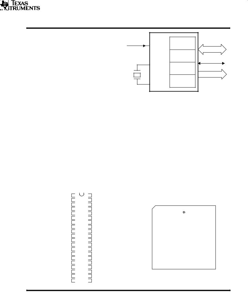
In addition to the above timings, tv must be taken into account. tv is the time that the data bus is guaranteed to be held after the rising edge of MWE or IOWE. In other ′C1x devices, the value of tv was referenced to CLKOUT↓ and not WE↑ (see Figure 12). For the ′C16, tv is a minimum of 5 ns. This implies that MWE and IOWE must be tied directly to the external device. If required, decode logic must be added to an input other than the read/write input Ð for example, the chip select on SRAMs. If the external device does not have two inputs, then transparent latches must be added to extend the time data is held on the data bus. These latches must be off the bus prior to the next instruction (see Figure 12).
CLKOUT
MWE or IOWE
tv td10
D15-D0
Figure 12.
where:
tv = 5 ns (min) td10 = 15 ns (max)
There is a potential for bus conflict on the prefetch and execution of a TBLW or an OUT instruction. Figure 13 details the timings to be considered. In addition to the timings for the ′C16, timing definitions for interface are also included.
Dummy Prefetch Cycle  TBLW or OUT Execution
CLKOUT
tddeco
MEN
tdmemh
CE
D15-D0
Memory Driven Data
td9(MEN)
tconf
D15-D0 DSP Driven Data
Figure 13.
where:
POST OFFICE BOX 1443 • HOUSTON, TEXAS 77001 |
91 |

TMS320C16
DIGITAL SIGNAL PROCESSORS
SPRS009C± JANUARY 1987 ± REVISED JULY 1991
tconf (data bus conflict time) = tddeco + tdmemh ± td9(MEN)
with: |
|
tddeco |
: decode delay time to make the CE or OE signal |
tdmemh |
: memory data hold time from CE or OE |
td9 |
: delay time, MEN to data bus starts being driven |
td9 |
: (at 35 MHz CLKIN) = [1/4tc(C)] = [1/4(114.3)] = 28.58 ns |
If tconf is less than or equal to zero, data bus conflict does not occur.
If tconf is greater than zero, data conflict occurs.
Note that the following discussion is for CLKIN of 35 MHz.
static memory with output enable and write enable/chip select
The following SRAMs are able to interface directly to the ′C16, needing only to directly connect the ′C16 memory control signals MEN and MWE to the memory. Device select decode is accomplished with address decode and then input to the device chip select.
PRODUCT |
tddeco |
tdmemh |
tdconf |
UNITS |
TC55645-35 |
0 |
15 |
±13.58 |
ns |
TC55328-35 |
0 |
15 |
±13.58 |
ns |
TMS6789-35 |
0 |
8 |
±20.58 |
ns |
TC5588-35 |
0 |
10 |
±18.58 |
ns |
TMS6716-35 |
0 |
10 |
±18.58 |
ns |
MWE |
|
WE |
|
MEN |
|
OE |
|
|
|
SRAM With OE |
|
TMS320C16 |
|
CS |
|
|
|
||
A15-AXX |
ALS138 |
ADDR |
|
(Decoder) |
|||
|
|
||
|
|
DATA |
D15-D0
Figure 14.
92 |
POST OFFICE BOX 1443 • HOUSTON, TEXAS 77001 |

TMS320C16
DIGITAL SIGNAL PROCESSOR
SPRS009C ± JANUARY 1987 ± REVISED JULY 1991
static memory with chip enable and write enable
Without a separate output enable, a faster SRAM is required. Logic is added to decode address and memory control to perform a read/write cycle. The MWE signal is directly connected to the WE input of the SRAM to meet the tv specification (see Figure 15).
Product |
tddeco |
tdmemh |
tdconf |
Units |
CY7C164-25 |
7.5 |
10 |
± 11.08 |
ns |
MWE |
|
Programmable |
|
WE |
|
Logic |
|
||
|
|
|
|
|
MEN |
|
7.5 ns |
|
CE |
|
|
|
||
TMS320C16 |
|
|
|
SRAM With CE |
A15-AXX |
|
|
|
ADDR |
|
|
|
|
DATA |
D15-D0 |
|
|
|
|
Figure 15.
EPROM interface
The following high-speed EPROMs can be used directly:
|
Product |
tddeco |
tdmemh |
tdconf |
Units |
|||||||
CY7C291-35 |
0 |
25 |
± 3.58 |
|
ns |
|||||||
TMS27C291-35 |
0 |
25 |
± 3.58 |
|
ns |
|||||||
|
|
|
|
|
|
|
|
|
|
|
|
|
|
|
|
|
|
|
|
|
|
|
|
|
|
|
|
MEN |
|
|
|
|
|
|
CS1 |
|
|
|
|
|
|
|
|
|
VCC |
|
|
CS2 |
|
|
|
|
TMS320C16 |
|
|
|
|
|
Fast EPROM |
|
||||
|
|
|
|
|
|
TMS27C291-35 |
|
|||||
|
|
|
|
|
|
|
|
|
|
|||
|
A15-AXX |
|
Decoder |
|
|
|
CS3 |
|
|
|||
|
|
|
|
|
|
|
|
|
||||
|
|
|
|
|
7.5 ns |
|
|
|
ADDR |
|
|
|
|
|
|
|
|
|
|
|
|
|
|
||
|
|
|
|
|
|
|
|
|
|
|
DATA |
|
D15-D0
Figure 16.
POST OFFICE BOX 1443 • HOUSTON, TEXAS 77001 |
93 |

TMS320C16
DIGITAL SIGNAL PROCESSOR
SPRS009C± JANUARY 1987 ± REVISED JULY 1991
interfacing latches to the TMS320C16
As with the previous devices, the memory control signal must be directly connected to the latch and the latch needs to have a separate chip select. There are several devices with this feature, including the SN74ALS996. The SN74ALS996 is an 8-bit D-type edge-triggered read-back latch with three-state outputs, connected to the ′C16 as illustrated in Figure 17.
D15-D0 |
|
D15-D0 |
|
IOWE |
|
CLK |
|
IOEN |
|
RD |
|
TMS320C16 |
ALS 138 |
ALS996A x 2 |
|
A2 |
|
||
Decoder |
|
||
A1 |
EN |
||
|
|||
A0 |
|
|
Figure 17.
94 |
POST OFFICE BOX 1443 • HOUSTON, TEXAS 77001 |
TMS320C17, TMS320E17, TMS320LC17, TMS320P17 DIGITAL SIGNAL PROCESSORS
SPRS009C ± JANUARY 1987 ± REVISED JULY 1991
Key Features: TMS320C17/E17/LC17/P17
•200-ns Instruction Cycle Timing (TMS320C17/E17/P17)
•278-ns Instruction Cycle Timing (TMS320LC17)
•256 Words of On-Chip Data RAM
•4K Words of On-Chip Program ROM (TMS320C17/LC17)
•4K Words of On-Chip Program EPROM (TMS320E17/P17)
Interrupt |
Dua-Channel |
|
Serial Port |
||
|
||
|
Data (16) |
|
|
Coprocessor |
|
′320C17 |
Interface |
|
Serial Interface |
||
or |
||
|
||
′320E17 |
µ-Law/A-Law |
|
|
Hardware |
|
|
Address (3) |
|
|
Timer |
• One-Time Programmable (OTP) Windowless |
• Device Packaging: |
||
EPROM Version Available (TMS320P17) |
Ð 40-Pin DIP (All Devices) |
||
• EPROM Code Protection for Copyright Security |
Ð |
44-Lead PLCC (TMS320C17/LC17/P17 |
|
• Dual-Channel Serial Port for Full-Duplex Serial |
Ð |
44-Lead CER-QUAD (TMS320E17) |
|
• 3.3 -V Low-Power Version Available |
|||
Communication |
|||
|
|
||
• Serial Port Timer for Standalone Serial |
(TMS320LC17) |
|
• Operating Free-Air Temperature Range |
||
Communication |
||
. . . 0°C to 70°C |
||
• On-Chip Companding Hardware for -law/A-law |
||
• 16-Bit Coprocessor Interface for Common |
||
PCM Conversions |
||
4/8/16/32-Bit Microcomputers/Microprocessors |
||
|
TMS320C17/E17/LC17/P17
N/JD Package
(Top View)
PA1/RBLE |
1 |
40 |
|
PA2/TBLF |
|||||||
PA0/HI/LO |
2 |
39 |
|
FSR |
|||||||
|
MC |
3 |
38 |
|
FSX |
||||||
|
RS |
4 |
37 |
|
FR |
||||||
|
EXINT |
|
5 |
36 |
|
DX1 |
|||||
CLKOUT |
6 |
35 |
|
DX0 |
|||||||
|
X1 |
7 |
34 |
|
SCLK |
||||||
X2/CLKIN |
8 |
33 |
|
DRI |
|
|
|
||||
|
BIO |
9 |
32 |
|
DEN |
/RD |
|
||||
|
VSS |
10 |
31 |
|
WE/RD |
||||||
D8/LD8 |
11 |
30 |
|
VCC |
|||||||
D9/LD9 |
12 |
29 |
|
DR0 |
|||||||
D10/LD10 |
13 |
28 |
|
XF |
|
|
|||||
D11/LD11 |
14 |
27 |
|
MC/PM |
|
||||||
D12/LD12 |
15 |
26 |
|
D0/LD0 |
|||||||
D13/LD13 |
16 |
25 |
|
D1/LD1 |
|||||||
D14/LD14 |
17 |
24 |
|
D2/LD2 |
|||||||
D15/LD15 |
18 |
23 |
|
D3/LD3 |
|||||||
D7/LD7 |
19 |
22 |
|
D4/LD4 |
|||||||
D6/LD6 |
20 |
21 |
|
D5/LD5 |
|||||||
TMS320C17, TMS320E17
FN/FZ Packages
(Top View)
|
|
|
|
EXINT RS MC |
|
|
PAO/HI/LO |
|
|
PA1/RBLE |
V |
|
PA2/TBLF FSR FSX FR |
|
DX1 |
|
|
|
|
|
||||||||||||||||
|
|
|
|
|
|
|
|
|
|
|
|
|
|
|
||||||||||||||||||||||
|
|
|
|
|
|
|
|
|
|
|
|
|
||||||||||||||||||||||||
|
|
|
|
|
|
|
|
|
|
|
|
|
||||||||||||||||||||||||
|
|
|
|
|
|
|
|
|
|
|
||||||||||||||||||||||||||
|
|
|
|
|
|
|
|
|
|
|
|
|
||||||||||||||||||||||||
|
|
|
|
|
|
|
|
|
|
|
|
|
|
|
|
|
|
SS |
|
|
|
|
|
|
|
|
|
|
|
|
|
|
|
|
|
|
|
|
|
|
|
|
|
|
|
|
|
|
|
|
|
|
|
|
|
|
|
|
|
|
|
|
|
|
|
|
|
|
|
|
|
||
|
|
|
|
|
|
|
|
|
|
|
|
|
|
|
|
|
|
|
|
|
|
|
|
|
|
|
|
|
|
|
|
|
|
|
|
|
|
|
|
|
|
|
|
|
|
|
|
|
|
|
|
|
|
|
|
|
|
|
|
|
|
|
|
|
|
|
|
|
|
|
|
|
|
|
6 |
5 |
4 |
3 |
|
2 |
|
1 44 43 42 41 40 |
|
|
|
|
|
|||||||||||||||||||||||
CLKOUT |
|
7 |
|
|
|
|
|
|
|
|
|
|
|
|
|
|
|
|
|
|
|
|
|
|
|
|
|
|
39 |
|
|
DX0 |
||||
|
|
|
|
|
|
|
|
|
|
|
|
|
|
|
|
|
|
|
|
|
|
|
|
|
|
|
|
|||||||||
X1 |
|
8 |
|
|
|
|
|
|
|
|
|
|
|
|
|
|
|
|
|
|
|
|
|
|
|
|
|
|
38 |
|
|
SCLK |
||||
|
|
|
|
|
|
|
|
|
|
|
|
|
|
|
|
|
|
|
|
|
|
|
|
|
|
|
|
|||||||||
X2/CLKIN |
|
9 |
|
|
|
|
|
|
|
|
|
|
|
|
|
|
|
|
|
|
|
|
|
|
|
|
|
|
37 |
|
|
DR1 |
||||
|
|
|
|
|
|
|
|
|
|
|
|
|
|
|
|
|
|
|
|
|
|
|
|
|
|
|
|
|||||||||
BIO |
|
10 |
|
|
|
|
|
|
|
|
|
|
|
|
|
|
|
|
|
|
|
|
|
|
|
|
|
|
36 |
|
|
DEN/RD |
||||
|
|
|
|
|
|
|
|
|
|
|
|
|
|
|
|
|
|
|
|
|
|
|
|
|
|
|
|
|||||||||
NC |
|
11 |
|
|
|
|
|
|
|
|
|
|
|
|
|
|
|
|
|
|
|
|
|
|
|
|
|
|
35 |
|
|
WE/WR |
||||
|
|
|
|
|
|
|
|
|
|
|
|
|
|
|
|
|
|
|
|
|
|
|
|
|
|
|
|
|||||||||
VSS |
|
12 |
|
|
|
|
|
|
|
|
|
|
|
|
|
|
|
|
|
|
|
|
|
|
|
|
|
|
34 |
|
|
VCC |
||||
|
|
|
|
|
|
|
|
|
|
|
|
|
|
|
|
|
|
|
|
|
|
|
|
|
|
|
|
|||||||||
|
|
|
|
|
|
|
|
|
|
|
|
|
|
|
|
|
|
|
|
|
|
|
|
|
|
|
|
|
|
|
|
|||||
D8 |
|
13 |
|
|
|
|
|
|
|
|
|
|
|
|
|
|
|
|
|
|
|
|
|
|
|
|
|
|
33 |
|
|
DR0 |
||||
D9 |
|
14 |
|
|
|
|
|
|
|
|
|
|
|
|
|
|
|
|
|
|
|
|
|
|
|
|
|
|
32 |
|
|
XF |
|
|
||
|
|
|
|
|
|
|
|
|
|
|
|
|
|
|
|
|
|
|
|
|
|
|
|
|
|
|
|
|||||||||
D10 |
|
15 |
|
|
|
|
|
|
|
|
|
|
|
|
|
|
|
|
|
|
|
|
|
|
|
|
|
|
31 |
|
|
MC/PM |
|
|||
|
|
|
|
|
|
|
|
|
|
|
|
|
|
|
|
|
|
|
|
|
|
|
|
|
|
|
|
|||||||||
D11 |
|
16 |
|
|
|
|
|
|
|
|
|
|
|
|
|
|
|
|
|
|
|
|
|
|
|
|
|
|
30 |
|
|
D0/LD0 |
||||
|
|
|
|
|
|
|
|
|
|
|
|
|
|
|
|
|
|
|
|
|
|
|
|
|
|
|
|
|||||||||
D12 |
|
17 |
|
|
|
|
|
|
|
|
|
|
|
|
|
|
|
|
|
|
|
|
|
|
|
|
|
|
29 |
|
|
VSS |
||||
|
|
|
|
|
|
|
|
|
|
|
|
|
|
|
|
|
|
|
|
|
|
|
|
|
|
|
|
|||||||||
18 19 20 21 22 23 24 25 26 27 28 |
|
|||||||||||||||||||||||||||||||||||
|
|
|
|
|
|
|||||||||||||||||||||||||||||||
|
|
|
|
|
|
|
|
|
|
|
|
|
|
|
|
|
|
|
|
|
|
|
|
|
|
|
|
|
|
|
|
|
|
|
|
|
|
|
V |
|
D13/LD13 |
|
D14/LD14 |
|
D15/LD15 |
D7/LD7 |
D6/LD6 |
D5/LD5 D4LD4 D3/LD3 D2/LD2 |
|
D1/LD1 |
|
|
|
|
|
||||||||||||||||||
|
|
|
SS |
|
|
|
|
|
|
|
|
|
|
|
|
|
|
|
|
|
|
|
|
|
|
|
|
|
|
|
|
|
|
|
|
|
POST OFFICE BOX 1443 • HOUSTON, TEXAS 77001 |
95 |

TMS320C17, TMS320E17, TMS320LC17, TMS320P17
DIGITAL SIGNAL PROCESSORS
SPRS009C± JANUARY 1987 ± REVISED JULY 1991
architecture
The ′C17/E17/LC17/P17 consists of five major functional units: the ′C15 microcomputer, a system control register, a full-duplex dual-channel serial port, companding hardware, and a coprocessor port.
Three of the I/O ports are used by the serial port, companding hardware, and the coprocessor port. Their operation is determined by the 32 bits of the system control register (see Table 6 for the control register bit definitions). Port 0 accesses control register 0 and consists of the lower 16 register bits (CR15-CR0), and is used to control the interrupts, serial port connections, and companding hardware operation. Port 1 accesses control register 1, consisting of the upper 16 control bits (CR31-CR16), as well as both serial port channels, the companding hardware, and the coprocessor port channels. Communication with the control register is via IN and OUT instructions to ports 0 and 1.
Interrupts fully support the serial port interface. Four maskable interrupts (EXINT, FR, FSX, and FSR) are mapped into I/O port 0 via control register 0. When disabled, these interrupts may be used as single-bit logic inputs polled by software.
serial port
The dual-channel serial port is capable of full-duplex serial communication and offers direct interface to two combo-codecs. Two receive and two transmit registers are mapped into I/O port 1, and operate with 8-bit data samples. Internal and external framing signals for serial port transfers (MSB first) are selected via the system control register. The serial port clock, SCLK, provides the bit timing for transfers with the serial port, and may be either an input or output. As an input, an external clock provides the timing for data transfers and framing pulse synchronization. As an output, SCLK provides the timing for standalone serial communication and is derived from the ′C17/E17/P17 system clock, X2/CLKIN, and system control register bits CR27-CR24 (see Table 7 for the available divide ratios). The internal framing (FR) pulse frequency is derived from the serial port clock (SCLK) and system control register bits CR23-CR16. This framing pulse signal provides framing pulses for combo-codecs, for a sample clock for voice-band systems, or for a timer used in control applications.
µ-law/A-law companding hardware
The ′C17/E17/LC17/P17 features hardware companding logic and can operate in either µ-law or A-law format with either sign-magnitude or twos-complement numbers. Data may be companded in either a serial mode for operation on serial port data or a parallel mode for computation inside the device. The companding logic operation is selected through CR14. No bias is required when operating in twos-complement. A bias of 33 is required for sign-magnitude in µ-law companding. Upon reset, the device is programmed to operate in sign-magnitude mode. This mode can be changed by modifying control bit 29 (CR29) in control register 1. For further information on companding, see the TCM29C13/TCM29C14/TCM29C16/TCM29C17 Combined Single-Chip PCM Codec and Filter Data Sheet, and the application report, ªCompanding Routines for the TMS32010/TMS32020,º in the book Digital Signal Processing Applications with the TMS320 Family
(SPRA012A), both documents published by Texas Instruments.
In the serial mode, sign-magnitude linear PCM (13 magnitude bits plus 1 sign bit for µ-law format or 12 magnitude bits plus 1 sign bit for A-law format) is compressed to 8-bit sign-magnitude logarithmic PCM by the encoder and sent to the transmit register for transmission on an active framing pulse. The decoder converts 8-bit sign-magnitude log PCM from the serial port receive registers to sign-magnitude linear PCM.
In the parallel mode, the serial port registers are disabled to allow parallel data from internal memory to be encoded or decoded for computation inside the device. In the parallel encode mode, the encoder is enabled and a 14-bit sign-magnitude value written to port 1. The encoded value is returned with an IN instruction from port 1. In the parallel decode mode, the decoder is enabled and an 8-bit sign-magnitude log PCM value is written to port 1. On the successive IN instruction from port 1, the decoded value is returned. At least one instruction should be inserted between an OUT and the successive IN when companding is performed with twos-complement values.
96 |
POST OFFICE BOX 1443 • HOUSTON, TEXAS 77001 |

TMS320C17, TMS320E17, TMS320LC17, TMS320P17
DIGITAL SIGNAL PROCESSORS
SPRS009C ± JANUARY 1987 ± REVISED JULY 1991
Table 6. Control Register Configuration
|
|
|
|
|
|
|
|
|
|
FR |
|
|
|
|
|
|
|
|
|
|
|
|
|
|
|
|
|
|
|
Port 1 |
|
Port 0 |
|
|
|
|
|
|
|
|
|
|
|
|
|
|
|
|
|
|
|
|
|
|
|
|
|
|
|
||||||
|
|
|
|
|
|
|
|
|
|
|
|
|
|
|
|
|
|
|
|
|
|
|
|
|
|
|
|
|
|
|
|
|
|
|
|
|
|
|
|
|
|
|
|
|
|
|
|
|
|
|
|
|
|
|
|
||||||||||
|
|
|
|
|
|
|
|
Pulse |
|
|
|
|
|
|
|
|
|
|
|
|
|
|
|
|
|
|
|
|
|
|
|
|
|
|
|
|
|
|
|
|
|
|
|
|
|
|
|
|
|
|
|
|
|
|
|
|
|
|
|
||||||
|
|
|
|
|
|
|
|
|
Widt |
|
|
|
|
|
|
|
|
|
Frame Counter Modulus |
|
|
|
|
|
|
|
|
|
|
|
|
|
|
|
Interrupt Mask Bits |
|
|
|
|
|
|
|
|||||||||||||||||||||||
|
|
|
|
|
|
|
|
|
|
|
h |
|
|
|
|
|
|
|
|
|
|
|
|
|
|
|
|
|
|
|
|
|
|
|
|
|
|
|
|
|
|
|
|
|
|
|
|
|
|
|
|
|
|
|
|
|
|
|
|
|
|
|
|
|
|
|
|
|
|
|
|
|
|
|
|
|
|
|
|
|
|
|
|
|
|
|
|
|
|
|
|
|
|
|
|
|
|
|
|
|
|
|
|
|
|
|
|
|
|
|
|
|
|
|
|
|
|
|
|
|
|
|
|
|
|
|
|
|
|
|
|
|
|
|
|
|
|
|
|
|
|
|
|
|
|
|
|
|
|
|
|
|
|
|
|
|
|
|
|
|
|
|
|
|
|
|
|
|
|
|
|
|
|
|
|
|
|
|
|
|
|
||||||||||||||||
|
31 |
30 |
|
|
29 |
|
28 |
27 |
26 |
|
25 |
24 |
|
|
23 |
22 |
21 |
20 |
|
19 |
18 |
17 |
|
16 |
15 |
14 |
|
13 |
12 |
|
11 |
10 |
9 |
|
8 |
|
7 |
|
6 |
5 |
4 |
|
|
3 |
2 |
|
1 |
0 |
|
||||||||||||||||
|
|
|
|
|
|
|
|
|
|
|
|
|
|
|
|
|
|
|
|
|
|
|
|
|
|
|
|
|
|
|
|
|
|
|
|
|
|
|
|
|
|
|
|
|
|
|
|
|
|
|
|
|
|
|
|
|
|
|
|
||||||
|
|
|
|
|
|
|
|
|
|
|
|
|
|
|
|
|
|
|
|
|
|
|
|
|
|
|
|
|
|
|
|
|
|
|
|
|
|
|
|
|
|
|
|
|
|
|
|
|
|
|
|
|
|
|
|
|
|
|
|
|
|
|
|
|
|
|
|
|
|
I/O |
|
|
|
|
|
Serial Clock |
|
|
|
|
|
|
|
|
|
|
|
|
|
|
|
|
Serial-Port Configuration |
|
|
|
|
|
|
|
|
|
|
Interrupt Flags |
|||||||||||||||||||||||||||
|
|
|
Control |
|
|
|
|
Prescale Control |
|
|
|
|
|
|
|
|
|
|
|
|
|
|
|
Companding Hardware Control |
|
|
|
|
|
|
|
|
|
|
|
|
|
|
|
||||||||||||||||||||||||||
|
|
|
|
|
|
|
|
|
|
|
|
|
|
|
|
|
|
|
|
|
|
|
|
|
|
|
|
|
|
|
|
|
|
|
|
|
|
|
|
|
|
|
|
|
|
|
|
|
|
|
|
|
|
|
|
|
|
|
|
|
|
|
|
|
|
Reserved |
|
|
|
|
|
|
|
|
|
|
|
|
|
|
|
|
|
|
|
|
|
|
|
|
|
|
|
|
|
|
|
|
|
|
|
|
|
|
|
|
|
|
|
|
|
|
|
|
|
|
|
|
|
|
|
|
|
|
|
||||||
|
|
|
|
|
|
|
|
|
|
|
|
|
|
|
|
|
|
|
|
|
|
|
|
|
|
|
|
|
|
|
|
|
|
|
|
|
|
|
|
|
|
|
|
|
|||||||||||||||||||||
|
|
|
|
BIT |
|
|
|
|
|
|
|
|
|
|
|
|
|
|
|
|
|
|
|
|
|
|
DESCRIPTION AND CONFIGURATION |
|
|
|
|
|
|
|
|
|
|
|
|
|
|
|
|
|
|||||||||||||||||||||
0EXINT Interrupt flag²
1FSR interrupt flag²
2FSX interrupt flag²
3FR interrupt flag²
4EXINT interrupt enable mask. When set to logic 1, an interrupt on EXINT activates device interrupt circuitry.
5FSR interrupt enable mask. Same as EXINT control.
6FSX interrupt enable mask. Same as EXINT control.
7FR interrupt enable mask. Same as EXINT control.
8 |
Port 1 configuration control: |
0 |
= port 1 connects to either serial-port registers or companding hardware. |
||||
1 |
= port 1 accesses CR31-CR16. |
||||||
|
|
||||||
|
|
|
|
|
|
||
9 |
External framing enable: |
0 |
= serial-port data transfers controlled by active FR. |
|
|
||
1 |
= serial-port data transfers controlled by active FSX/FSR. |
||||||
|
|||||||
|
|
|
|
|
|||
10 |
XF external logic output flag latch |
|
|
|
|||
|
|
||||||
11 |
0 = Parallel companding mode; serial port disabled. |
||||||
Serial-port enable: 1 = serial companding mode; serial port registers enabled. |
|||||||
|
|||||||
12 |
-law/A-law encoder enable: |
0 |
= disabled. |
|
|
|
|
1 |
= data written to port 1 is -law or A-law encoded. |
||||||
|
|||||||
|
|
|
|
|
|
|
|
13 |
|
0 |
= disabled. |
|
|
|
|
-law/A-law decoder enable: |
1 |
= data written to port 1 is -law or A-law decoded. |
|||||
|
|||||||
|
|
|
|
|
|||
14 |
|
|
|
0 = companding hardware performs -law conversion. |
|||
-law/A-law decoder encode/decoded select: |
1 = companding hardware performs A-law conversion. |
||||||
|
|||||||
15
0 = SCLK is an output, derived from the prescaler in timing logic.
Serial clock control: 1 = SCLK is an input that provides the clock for serial port and frame counter in timing logic.
23-16 |
Frame counter modulus. Controls FR frequency = SCLK/(CNT + 2) where CNT is binary value fo CR23-CR16³ |
|||
27-24 |
SCLK prescale cotnrol bits. (See Table 7 for divide ratios.) |
|||
|
|
|
|
|
28 |
|
0 |
= fixed-data rate; FR is 1 SCLK cycle wide. |
|
FR pulse-width control: |
1 |
= variable-data rate; FR is 8 SCLK cycles wide. |
||
|
||||
|
|
|
||
29
0 = sign-magnitude companding
Two's-complement -law/A-law conversion enable: 1 = twos-complement companding
30
0 = 8-bit byte length
1 = 16-bit word length
8/16-bit length coprocessor mode select:
31Reserved for future expansion: Should be set to zero.
²Interrupt flag is cleared by writing a logic 1 to the bit with an OUT instruction to port 0.
³All ones in CR23-CR16 indicate a degenerative state and should be avoided. Bits are operational whether SCLK is an input or an output. CNT must be greater than 7.
POST OFFICE BOX 1443 • HOUSTON, TEXAS 77001 |
97 |

TMS320C17, TMS320E17, TMS320LC17, TMS320P17
DIGITAL SIGNAL PROCESSORS
SPRS009C± JANUARY 1987 ± REVISED JULY 1991
Table 7. Serial Clock (SCLK) Divide Ratios (X2/CLKIN = 20.48 MHz)
CR27 |
CR26 |
CR25 |
CR24 |
DIVIDE RATIO |
SCLK FREQUENCY |
UNIT |
|
|
|
|
|
|
|
0 |
0 |
0 |
0 |
32 |
0.640 |
MHz |
|
|
|
|
|
|
|
0 |
0 |
0 |
1 |
28 |
0.731 |
MHz |
|
|
|
|
|
|
|
0 |
0 |
1 |
0 |
24 |
0.853 |
MHz |
|
|
|
|
|
|
|
0 |
1 |
0 |
0 |
20 |
1.024 |
MHz |
|
|
|
|
|
|
|
1 |
0 |
0 |
0 |
16 |
1.280 |
MHz |
|
|
|
|
|
|
|
1 |
0 |
0 |
1 |
14 |
1.463 |
MHz |
|
|
|
|
|
|
|
1 |
0 |
1 |
0 |
12 |
1.706 |
MHz |
|
|
|
|
|
|
|
1 |
1 |
0 |
0 |
10 |
2.048 |
MHz |
The specification for µ-law and A-law log PCM coding is part of the CCITT G.711 recommendation. The following diagram shows a ′C17/E17/P17 interface to two codecs as used for µ-law or A-law companding format.
|
TMS320C17/E17/P17 |
|
|
|
|
|
|
TCM29C13 |
|
|
|
DX0 |
PCM In |
Analog Out |
|
VSS |
DR0 |
PCM Out |
Analog In |
|
|
|
|
|
|
|
SCLK |
CLKR/X |
|
+5 V |
VCC |
FR |
FSX |
|
|
MC |
|
FSR |
|
|
MC/PM |
|
|
|
|
X2 |
|
TCM29C13 |
|
|
DX1 |
PCM In |
Analog Out |
|
|
|
|||
|
|
DR1 |
PCM Out |
Analog In |
X1
CLKR/X
FSX
FSR
coprocessor port
The coprocessor port, accessed through I/O port 5 using IN and OUT instructions, provides a direct connection to most 4/8-bit microcomputers and 16/32-bit micorprocessors. The coprocessor interface allows the ′C17/E17/P17 to act as a peripheral (slave) microcomputer to a microprocessor, or a master to a peripheral microcomputer such as TMS7042. The coprocessor port is enabled by setting MC/PM and MC low. The microcomputer mode is enabled by setting these two pins high. (Note that MC/PM ≠ MC is undefined.)
In the microcomputer mode, the 16 data lines are used for the 6 parallel 16-bit I/O ports.
In the coprocessor mode, the 16-bit coprocessor port is reconfigured to operate as a 16-bit latched bus interface. Control bit 30 (CR30) in control register 1 is used to configure the coprocessor port to either an 8-bit or a 16-bit length. When CR30 is high, the coprocessor port is 16 bits wide thereby making all 16 bits of the data port available for 16-bit transfers to 16 and 32-bit microprocessors. When CR30 is low, the port is 8-bits wide and mapped to the low byte of the data port for interfacing to 8-bit microcomputers. When operating in the 8-bit mode, both halves of the 16-bit latch can be addressed using the HI/LO pin, thus allowing 16-bit transfers over 8 data lines. When not in the coprocessor mode, port 5 can be used as a generic I/O port.
98 |
POST OFFICE BOX 1443 • HOUSTON, TEXAS 77001 |

TMS320C17, TMS320E17
DIGITAL SIGNAL PROCESSORS
SPRS009C ± JANUARY 1987 ± REVISED JULY 1991
coprocessor port (continued)
The external processor recognizes the coprocessor interface in which both processors run asynchronously as a memory-mapped I/O operation. The external processor lowers the WR line and places data on the bus. It next raises the WR line to clock the data into the on-chip latch. The rising edge of WR automatically creates an interrupt to the ′C17/E17/P17, and the falling edge of WR clears the RBLE (receive buffer latch empty) flag. When the ′C17/E17/P17 reads the coprocessor port, it causes the RBLE signal to transition to a logic low state that clears the data in the latch, and allows the interrupt condition to be cleared internally. Likewise, the external processor reads form the latch by driving the RD line active low, thus enabling the output latch to drive the latched data. When the data has been read, the external device will again bring the RD line high. This activates the BIO line to signal that the transfer is complete and the latch is available for the next transfer. The falling edge of RD resets the TBLF (transmit buffer latch full) flag. Note that the EXINT and BIO lines are reserved for coprocessor interface and cannot be driven externally when in the coprocessor mode.
An example of the use of a coprocessor interface is shown in Figure 18, in which the ′C17/E17/P17 are DSPs interfaced to the TMS70C42, an 8-bit microcontroller.
TMS320C17/E17/P17 |
|
|
|
|
|
|
TMS70C42 |
|||||||
|
|
|
MC |
3 |
|
|
|
|
|
|
||||
|
|
|
27 |
|
|
|
|
|
|
|||||
|
|
|
|
|
|
|
|
|
|
|
|
|
||
MC/PM |
|
|
|
|
||||||||||
2 |
|
|
|
|
|
|
||||||||
|
|
|
|
|
|
|
|
|
|
|
|
|
||
|
HI/LO |
|
|
|
|
|||||||||
|
|
|
|
|
|
|
|
|||||||
|
|
|
|
|
|
|
|
|
|
|
|
|
|
|
|
|
|
|
|
|
|
|
|
|
|
|
|
|
|
|
|
|
|
|
|
|
6 |
|
|
17 |
|
|||
CLKOUT |
XTAL2 |
|||||||||||||
31 |
|
|
7 |
|||||||||||
|
|
|
|
|
|
|
|
|
A1 |
|||||
|
|
WR |
||||||||||||
|
|
1 |
|
|
6 |
|||||||||
|
|
|
|
|
|
|
|
|
|
|||||
|
RBLE |
A0 |
||||||||||||
|
32 |
|
|
9 |
||||||||||
|
|
|
|
|
|
|
|
|
A3 |
|||||
|
|
|
|
RD |
||||||||||
|
|
|
|
40 |
|
|
8 |
|||||||
|
|
|
|
|
|
|
|
|
|
|||||
|
|
TBLF |
A2 |
|||||||||||
|
|
19 |
|
|
19 |
|||||||||
|
|
LD7 |
|
|
D7 |
|||||||||
|
|
|
|
|
|
|
|
|||||||
|
|
20 |
|
|
20 |
|||||||||
|
|
LD6 |
|
|
D6 |
|||||||||
|
|
21 |
|
|
21 |
|||||||||
|
|
LD5 |
|
|
D5 |
|||||||||
|
|
22 |
|
|
22 |
|||||||||
|
|
LD4 |
|
|
D4 |
|||||||||
|
|
23 |
|
|
23 |
|||||||||
|
|
LD3 |
|
|
D3 |
|||||||||
|
|
|
|
|
|
|
|
|||||||
|
|
24 |
|
|
24 |
|||||||||
|
|
LD2 |
|
|
D2 |
|||||||||
|
|
25 |
|
|
26 |
|||||||||
|
|
LD1 |
|
|
D1 |
|||||||||
|
|
|
|
|
|
|
|
|||||||
|
|
26 |
|
|
27 |
|||||||||
|
|
LD0 |
|
|
D0 |
|||||||||
|
|
|
|
|
|
|
|
|||||||
|
|
|
|
|
|
|
|
|||||||
|
|
|
|
|
|
|
|
|
|
|
|
|
|
|
Figure 18. Coprocessor Interface
POST OFFICE BOX 1443 • HOUSTON, TEXAS 77001 |
99 |

TMS320C17, TMS320E17, TMS320LC17, TMS320P17
DIGITAL SIGNAL PROCESSORS
SPRS009C± JANUARY 1987 ± REVISED JULY 1991
|
|
|
|
|
|
|
|
|
|
|
|
|
|
|
|
|
|
TERMINAL FUNCTIONS² |
||
|
|
|
|
|
|
|
|
|
|
|
|
|
|
|
|
|
|
|
|
|
|
|
|
|
|
|
|
|
|
|
|
|
|
|
|
|
NAME |
I/O³ |
DEFINITION |
||
|
|
|
|
|
|
|
|
|
|
|
|
|
|
|
|
|
I |
External polling input |
||
|
BIO |
|
|
|
|
|
|
|
|
|
|
|
|
|
||||||
|
CLKOUT |
O |
System clock output, 1/4 crystal/CLKIN frequency |
|||||||||||||||||
|
D15/LD15-D0/LD0 |
I/O |
16-bit parallel data bus/data lines for coprocessor latch |
|||||||||||||||||
|
|
|
|
|
|
|
|
|
|
|
|
|
|
|
|
I/O |
Data enable for device input data/external read for output latch |
|||
|
DEN/RD |
|||||||||||||||||||
|
DR1, DR0 |
I |
Serial-port receive-channel inputs |
|||||||||||||||||
|
DX1, DX0 |
O |
Serial-port transmit-channel outputs |
|||||||||||||||||
|
|
|
|
|
|
|
|
|
|
|
|
|
|
I |
External interrupt input |
|||||
|
EXINT |
|
|
|
|
|
|
|
||||||||||||
|
FR |
O |
Internal serial-port framing output |
|||||||||||||||||
|
|
|
|
|
|
|
|
|
|
|
|
|
|
I |
External serial-port receive framing input |
|||||
|
FSR |
|
|
|
|
|
|
|
||||||||||||
|
|
|
|
|
|
|
|
|
|
|
|
|
I |
External serial-port transmit framing input |
||||||
|
FSX |
|
|
|
|
|
|
|
|
|||||||||||
|
MC |
I |
|
|
|
|||||||||||||||
|
Microcomputer select (must be same state as MC/PM) |
|
||||||||||||||||||
|
|
|
|
|
|
|
|
|
|
|
|
|
I |
Microcomputer/peripheral coprocessor select (must be same state as MC) |
||||||
|
MC/PM |
|
|
|
|
|
|
|||||||||||||
|
|
|
|
|
|
|
|
|
|
|
I/O |
I/O port address output/latch byte select pin |
||||||||
|
PA0/HI/LO |
|
|
|||||||||||||||||
|
|
|
|
|
|
|
|
|
O |
I/O port address output/receive buffer latch empty flag |
||||||||||
|
PA1/RBLE |
|
||||||||||||||||||
|
|
|
|
|
|
|
|
O |
I/O port address output/transmit buffer latch full flag |
|||||||||||
|
PA2/TBLF |
|
||||||||||||||||||
|
|
|
|
|
I |
Reset for initializing the device |
||||||||||||||
|
RS |
|
|
|
|
|||||||||||||||
|
SCLK |
I/O |
Serial-port clock |
|||||||||||||||||
|
VCC |
I |
+ 5 V Supply |
|||||||||||||||||
|
VSS |
I |
Ground |
|||||||||||||||||
|
|
|
|
|
O |
Write enable for device output data/external write for input latch |
||||||||||||||
|
WE/WR |
|||||||||||||||||||
|
X1 |
O |
Crystal output for internal oscillator |
|||||||||||||||||
|
X2/CLKIN |
I |
Crystal input for internal oscillator or external oscillator system clock input |
|||||||||||||||||
|
XF |
O |
External-flag output pin |
|||||||||||||||||
|
|
|
|
|
|
|
|
|
|
|
|
|
|
|
|
|
|
|
|
|
² See EPROM programming section. ³ Input/Output/High-impedance state.
100 |
POST OFFICE BOX 1443 • HOUSTON, TEXAS 77001 |