

ADSP-2104/ADSP-2109
TIMING PARAMETERS (ADSP-2104/ADSP-2109)
CLOCK SIGNALS & RESET
|
|
|
|
|
Frequency |
|
|
|
|
|
|
20 MHz |
Dependency |
|
|
Parameter |
Min |
Max |
Min |
Max |
Unit |
||
|
|
|
|
|
|
|
|
Timing Requirement: |
|
|
|
|
|
||
tCK |
CLKIN Period |
50 |
150 |
|
|
ns |
|
tCKL |
CLKIN Width Low |
20 |
|
20 |
|
ns |
|
tCKH |
CLKIN Width High |
20 |
|
20 |
|
ns |
|
tRSP |
RESET |
Width Low |
250 |
|
5tCK1 |
|
ns |
Switching Characteristic: |
|
|
|
|
|
||
tCPL |
CLKOUT Width Low |
15 |
|
0.5tCK – 10 |
|
ns |
|
tCPH |
CLKOUT Width High |
15 |
|
0.5tCK – 10 |
|
ns |
|
tCKOH |
CLKIN High to CLKOUT High |
0 |
20 |
|
|
ns |
|
NOTE
1Applies after powerup sequence is complete. Internal phase lock loop requires no more than 2000 CLKIN cycles, assuming stable CLKIN (not including crystal
oscillator startup time).
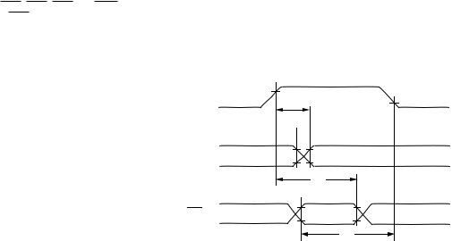
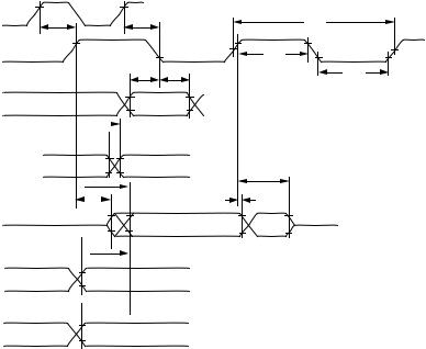
tCK
tCKH
CLKIN
tCKL
tCKOH
 tCPH
tCPH 
CLKOUT
 tCPL
tCPL 
Figure 19. Clock Signals
REV. 0 |
–21– |
ADSP-2104/ADSP-2109
TIMING PARAMETERS (ADSP-2104/ADSP-2109)
INTERRUPTS & FLAGS
|
|
|
|
|
|
|
Frequency |
|
|
|
|
|
|
|
|
20 MHz |
Dependency |
|
|
Parameter |
|
|
Min |
Max |
Min |
Max |
Unit |
||
|
|
|
|
|
|
|
|||
Timing Requirement: |
|
|
|
|
|
||||
tIFS |
IRQx |
1 |
or FI Setup before |
27.5 |
|
0.25tCK + 15 |
|
ns |
|
|
|
|
|||||||
|
CLKOUT Low2, 3 |
|
|
|
|
|
|||
tIFH |
|
1 |
or FI Hold after CLKOUT |
12.5 |
|
0.25tCK |
|
ns |
|
|
|
|
|||||||
IRQx |
|
|
|
||||||
|
High2, 3 |
|
|
|
|
|
|||
Switching Characteristic: |
|
|
|
|
|
||||
tFOH |
FO Hold after CLKOUT High |
0 |
|
0 |
|
ns |
|||
tFOD |
FO Delay from CLKOUT High |
|
15 |
|
|
ns |
|||
NOTES
1IRQx=IRQ0, IRQ1, and IRQ2.
2If IRQx and FI inputs meet tIFS and tIFH setup/hold requirements, they will be recognized during the current clock cycle; otherwise they will be recognized during the following cycle. (Refer to the “Interrupt Controller” section in Chapter 3, Program Control, of the ADSP-2100 Family User’s Manual for further information on interrupt servicing.)
3Edge-sensitive interrupts require pulse widths greater than 10 ns. Level-sensitive interrupts must be held low until serviced.
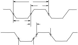
CLKOUT |
tFOD |
|
tFOH 

FLAG
OUTPUT(S)
tI F H
IRQx
FI
tI F S
Figure 20. Interrupts & Flags
–22– |
REV. 0 |
ADSP-2104/ADSP-2109
TIMING PARAMETERS (ADSP-2104/ADSP-2109)
BUS REQUEST/GRANT
|
|
|
|
|
|
|
|
|
|
|
|
|
|
|
|
|
|
|
|
|
|
|
|
|
|
|
|
|
|
|
|
|
|
|
|
Frequency |
|
|
|
|
|
|
|
|
|
|
|
|
|
|
|
|
|
|
|
|
|
|
|
|
|
|
|
|
|
|
|
|
|
|
|
|
|
20 MHz |
Dependency |
|
|
Parameter |
Min |
Max |
Min |
Max |
Unit |
|||||||||||||||||||||||||||||||||
|
|
|
|
|
|
|
|
|
|
|
|
|
|
|
|
|
|
|
|
|
|
|
|
|
|
|
|
|
|
|
|
|
|
|
|
|
|
|
Timing Requirement: |
|
|
|
|
|
|||||||||||||||||||||||||||||||||
tBH |
BR |
|
Hold after CLKOUT High1 |
17.5 |
|
0.25tCK + 5 |
|
ns |
||||||||||||||||||||||||||||||
tBS |
BR |
|
Setup before CLKOUT Low1 |
32.5 |
|
0.25tCK + 20 |
|
ns |
||||||||||||||||||||||||||||||
Switching Characteristic: |
|
|
|
|
|
|||||||||||||||||||||||||||||||||
tSD |
CLKOUT High to |
DMS, |
|
|
|
32.5 |
|
0.25tCK + 20 |
ns |
|||||||||||||||||||||||||||||
|
PMS, |
|
|
|
|
BMS, |
|
|
|
RD, |
|
WR |
Disable |
|
|
|
|
|
||||||||||||||||||||
tSDB |
DMS, |
|
|
PMS, |
|
|
BMS, |
|
|
RD, |
|
|
WR |
|
0 |
|
0 |
|
ns |
|||||||||||||||||||
|
Disable to |
BG |
Low |
|
|
|
|
|
||||||||||||||||||||||||||||||
tSE |
BG |
High to |
DMS, |
|
PMS, |
|
0 |
|
0 |
|
ns |
|||||||||||||||||||||||||||
|
BMS, |
|
|
RD, |
|
WR |
Enable |
|
|
|
|
|
||||||||||||||||||||||||||
tSEC |
DMS, |
|
PMS, |
|
BMS, |
|
RD, |
|
WR |
|
2.5 |
|
0.25tCK – 10 |
|
ns |
|||||||||||||||||||||||
|
Enable to CLKOUT High |
|
|
|
|
|
||||||||||||||||||||||||||||||||
|
|
|
|
|
|
|
|
|
|
|
|
|
|
|
|
|
|
|
|
|
|
|
|
|
|
|
|
|
|
|
|
|
|
|
|
|
|
|
NOTES
1If BR meets the tBS and tBH setup/hold requirements, it will be recognized in the current processor cycle; otherwise it is recognized in the following cycle. BR requires a pulse width greater than 10 ns.
Note: BG is asserted in the cycle after BR is recognized. No external synchronization circuit is needed when BR is generated as an asynchronous signal.
|
tBH |
|
CLKOUT |
|
|
BR |
|
|
|
|
tBS |
CLKOUT |
|
|
PMS, DMS |
|
|
BMS, RD |
tSD |
tSEC |
WR |
|
|
BG |
|
tSDB |
|
|
|
|
|
tSE |
Figure 21. Bus Request/Grant
REV. 0 |
–23– |
ADSP-2104/ADSP-2109
TIMING PARAMETERS (ADSP-2104/ADSP-2109)
MEMORY READ
|
|
|
|
|
|
|
|
|
|
|
|
|
|
|
|
|
|
|
|
|
|
|
|
|
|
|
|
20 MHz |
|
Parameter |
Min |
Max |
Unit |
||||||||||||||||||||||||||
|
|
|
|
|
|
|
|
|
|
|
|
|
|
|
|
|
|
|
|
|
|
|
|
|
|
|
|
|
|
Timing Requirement: |
|
|
|
||||||||||||||||||||||||||
tRDD |
RD |
Low to Data Valid |
|
12 |
ns |
||||||||||||||||||||||||
tAA |
A0–A13, PMS, DMS, |
BMS |
|
to Data Valid |
|
19.5 |
ns |
||||||||||||||||||||||
tRDH |
Data Hold from |
RD |
|
High |
0 |
|
|
||||||||||||||||||||||
Switching Characteristic: |
|
|
|
||||||||||||||||||||||||||
tRP |
RD |
Pulse Width |
17 |
|
ns |
||||||||||||||||||||||||
tCRD |
CLKOUT High to |
RD |
|
Low |
7.5 |
22.5 |
ns |
||||||||||||||||||||||
tASR |
A0–A13, |
PMS, |
|
|
DMS, |
|
|
BMS |
Setup before |
2.5 |
|
ns |
|||||||||||||||||
|
RD Low |
|
|
|
|||||||||||||||||||||||||
tRDA |
A0–A13, |
PMS, |
|
DMS, |
|
BMS |
Hold after |
RD |
|
3.5 |
|
ns |
|||||||||||||||||
|
Deasserted |
|
|
|
|||||||||||||||||||||||||
tRWR |
RD High to |
RD |
or |
WR |
Low |
20 |
|
ns |
|||||||||||||||||||||
|
|
|
|
|
|
|
|
|
|
|
|
|
|
|
Frequency Dependency |
|
|
|
|
|
|
|
|
|
|
|
|
|
|
|
|
|
(CLKIN ≤ 20 MHz) |
|
|
Parameter |
Min |
Max |
Unit |
||||||||||||||
|
|
|
|
|
|
|
|
|
|
|
|
|
|
|
|
|
|
Timing Requirement: |
|
|
|
||||||||||||||
tRDD |
RD |
Low to Data Valid |
|
0.5tCK – 13 + w |
ns |
||||||||||||
tAA |
A0–A13, |
|
|
|
|
|
|
|
|
|
|
|
|
|
0.75tCK – 18 + w |
ns |
|
PMS, |
DMS, BMS to Data Valid |
|
|||||||||||||||
tRDH |
Data Hold from RD High |
0 |
|
|
|||||||||||||
Switching Characteristic: |
|
|
|
||||||||||||||
tRP |
RD |
Pulse Width |
0.5tCK – 8 + w |
|
ns |
||||||||||||
tCRD |
CLKOUT High to |
RD |
Low |
0.25tCK – 5 |
0.25tCK + 10 |
ns |
|||||||||||
tASR |
A0–A13, |
PMS, |
|
DMS, |
|
BMS |
Setup before |
|
|
|
|||||||
|
RD |
Low |
0.25tCK – 10 |
|
ns |
||||||||||||
tRDA |
A0–A13, |
PMS, |
|
DMS, |
|
BMS |
Hold after |
RD |
|
|
|
|
|||||
|
Deasserted |
0.25tCK – 9 |
|
ns |
|||||||||||||
tRWR |
RD |
High to |
RD |
or |
WR |
Low |
0.5tCK – 5 |
|
ns |
||||||||
NOTE
w = wait states × tCK.
CLKOUT
A0 – A13
DMS, PMS
BMS
RD
D
|
|
tRDA |
tASR |
tRP |
tRWR |
tCRD |
|
|
|
tRDD |
tRDH |
|
tAA |
|
WR
Figure 22. Memory Read
–24– |
REV. 0 |
ADSP-2104/ADSP-2109
TIMING PARAMETERS (ADSP-2104/ADSP-2109)
MEMORY WRITE
|
|
|
|
|
|
|
|
|
|
|
|
|
|
|
|
|
|
|
|
|
|
|
|
|
|
|
|
|
|
20 MHz |
|
Parameter |
Min |
Max |
Unit |
||||||||||||||||||||||||||||
|
|
|
|
|
|
|
|
|
|
|
|
|
|
|
|
|
|
|
|
|
|
|
|
|
|
|
|
|
|
|
|
Switching Characteristic: |
|
|
|
||||||||||||||||||||||||||||
tDW |
Data Setup before |
WR |
High |
12 |
|
ns |
|||||||||||||||||||||||||
tDH |
Data Hold after |
WR |
|
|
High |
2.5 |
|
ns |
|||||||||||||||||||||||
tWP |
WR Pulse Width |
17 |
|
ns |
|||||||||||||||||||||||||||
tWDE |
WR |
|
Low to Data Enabled |
0 |
|
ns |
|||||||||||||||||||||||||
tASW |
A0–A13, |
DMS, |
|
|
PMS |
Setup before |
2.5 |
|
ns |
||||||||||||||||||||||
|
WR Low |
|
|
|
|||||||||||||||||||||||||||
tDDR |
Data Disable before |
WR |
or |
RD |
|
Low |
2.5 |
|
ns |
||||||||||||||||||||||
tCWR |
CLKOUT High to |
WR |
|
Low |
7.5 |
22.5 |
ns |
||||||||||||||||||||||||
tAW |
A0–A13, DMS, |
PMS, |
Setup before |
WR |
|
15.5 |
|
ns |
|||||||||||||||||||||||
|
Deasserted |
|
|
|
|||||||||||||||||||||||||||
tWRA |
A0–A13, |
DMS, |
|
PMS |
Hold after |
WR |
|
3.5 |
|
ns |
|||||||||||||||||||||
|
Deasserted |
|
|
|
|||||||||||||||||||||||||||
tWWR |
WR |
High to |
RD |
or |
WR |
Low |
20 |
|
ns |
||||||||||||||||||||||
|
|
|
|
|
|
|
|
|
|
|
|
|
|
|
|
|
|
|
|
|
|
|
|
|
|
|
Frequency Dependency |
|
|
|
|
|
|
|
|
|
|
|
|
|
|
|
|
|
|
|
|
|
|
|
|
|
|
|
|
|
(CLKIN ≤ 20 MHz) |
|
|
Parameter |
Min |
Max |
Unit |
||||||||||||||||||||||||||
|
|
|
|
|
|
|
|
|
|
|
|
|
|
|
|
|
|
|
|
|
|
|
|
|
|
|
|
|
|
Switching Characteristic: |
|
|
|
||||||||||||||||||||||||||
tDW |
Data Setup before |
WR |
High |
0.5tCK – 13 + w |
|
ns |
|||||||||||||||||||||||
tDH |
Data Hold after |
WR |
|
High |
0.25tCK – 10 |
|
ns |
||||||||||||||||||||||
tWP |
WR |
|
Pulse Width |
0.5tCK – 8 + w |
|
ns |
|||||||||||||||||||||||
tWDE |
WR Low to Data Enabled |
0 |
|
|
|||||||||||||||||||||||||
tASW |
A0–A13, |
DMS, |
|
PMS |
Setup before |
WR |
|
Low |
0.25tCK – 10 |
|
ns |
||||||||||||||||||
tDDR |
Data Disable before |
WR |
or |
RD |
Low |
0.25tCK – 10 |
|
ns |
|||||||||||||||||||||
tCWR |
CLKOUT High to |
WR |
|
Low |
0.25tCK – 5 |
0.25tCK + 10 |
ns |
||||||||||||||||||||||
tAW |
A0–A13, |
DMS, |
|
PMS, |
Setup before |
WR |
|
|
|
|
|||||||||||||||||||
tWRA |
Deasserted |
0.75tCK – 22 + w |
|
ns |
|||||||||||||||||||||||||
A0–A13, |
DMS, |
|
PMS |
Hold after |
WR |
|
|
|
|
||||||||||||||||||||
|
Deasserted |
0.25tCK – 9 |
|
ns |
|||||||||||||||||||||||||
tWWR |
WR |
High to |
RD |
or |
WR |
Low |
0.5tCK – 5 |
|
ns |
||||||||||||||||||||
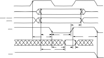
CLKOUT
A0 – A13
DMS, PMS
|
|
tWRA |
|
WR |
|
|
|
tASW |
|
tWP |
tWWR |
tCWR |
tAW |
tDH |
tDDR |
|
|||
|
|
|
|
D |
|
|
|
|
tWDE |
tDW |
|
|
|
|
RD
Figure 23. Memory Write
REV. 0 |
–25– |
ADSP-2104/ADSP-2109
TIMING PARAMETERS (ADSP-2104/ADSP-2109)
SERIAL PORTS
|
|
|
|
Frequency |
|
|
|
|
|
13.824 MHz* |
Dependency |
|
|
Parameter |
Min |
Max |
Min |
Max |
Unit |
|
|
|
|
|
|
|
|
Timing Requirement: |
|
|
|
|
|
|
tSCK |
SCLK Period |
72.3 |
|
|
|
ns |
tSCS |
DR/TFS/RFS Setup before SCLK Low |
8 |
|
|
|
ns |
tSCH |
DR/TFS/RFS Hold after SCLK Low |
10 |
|
|
|
ns |
tSCP |
SCLKIN Width |
28 |
|
|
|
ns |
Switching Characteristic: |
|
|
|
|
|
|
tCC |
CLKOUT High to SCLKOUT |
18.1 |
33.1 |
0.25tCK |
0.25tCK + 15 |
ns |
tSCDE |
SCLK High to DT Enable |
0 |
|
|
|
ns |
tSCDV |
SCLK High to DT Valid |
|
20 |
|
|
ns |
tRH |
TFS/RFSOUT Hold after SCLK High |
|
|
|
|
ns |
tRD |
TFS/RFSOUT Delay from SCLK High |
|
20 |
|
|
ns |
tSCDH |
DT Hold after SCLK High |
|
|
|
|
ns |
tTDE |
TFS (Alt) to DT Enable |
|
|
|
|
ns |
tTDV |
TFS (Alt) to DT Valid |
|
18 |
|
|
ns |
tSCDD |
SCLK High to DT Disable |
|
25 |
|
|
ns |
tRDV |
RFS (Multichannel, Frame Delay Zero) |
|
20 |
|
|
ns |
|
to DT Valid |
|
|
|
|
|
|
|
|
|
|
|
|
*Maximum serial port operating frequency is 13.824 MHz.
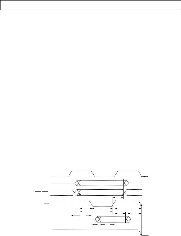
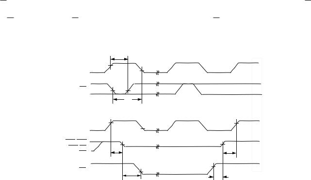
CLKOUT |
tCC |
tCC |
tSCK |
|
|||
SCLK |
|
|
tSCP |
|
|
|
|
|
|
tSCS tSCH |
tSCP |
DR
RFSIN
TFSIN
tRD  tRH
tRH 

RFSOUT
TFSOUT
tSCDD
tSCDV
tSCDE |
|
tSCDH |
|
DT
tTDE 

tTDV 
TFS
( ALTERNATE FRAME MODE )
 tRDV
tRDV 
RFS
( MULTICHANNEL MODE, FRAME DELAY 0 {MFD = 0} )
Figure 24. Serial Ports
–26– |
REV. 0 |

ADSP-2104/ADSP-2109
TIMING PARAMETERS (ADSP-2104L/ADSP-2109L)
GENERAL NOTES
Use the exact timing information given. Do not attempt to derive parameters from the addition or subtraction of others. While addition or subtraction would yield meaningful results for an individual device, the values given in this data sheet reflect statistical variations and worst cases. Consequently, you cannot meaningfully add parameters to derive longer times.
TIMING NOTES
Switching characteristics specify how the processor changes its signals. You have no control over this timing—circuitry external to the processor must be designed for compatibility with these signal characteristics. Switching characteristics tell you what the processor will do in a given circumstance. You can also use switching characteristics to ensure that any timing requirement of a device connected to the processor (such as memory) is satisfied.
Timing requirements apply to signals that are controlled by circuitry external to the processor, such as the data input for a read operation. Timing requirements guarantee that the processor operates correctly with other devices.
MEMORY REQUIREMENTS
The table below shows common memory device specifications and the corresponding ADSP-2104L/ADSP-2109L timing parameters, for your convenience.
|
|
ADSP-2104L/ADSP-2109L |
|
|
|
|
|
|
|
|
|
|
|
|
|
|
|
|
|
Memory Specification |
Timing Parameter |
Timing Parameter Definition |
|||||||||||||||||
|
|
|
|
|
|
|
|
|
|
|
|
|
|
|
|
|
|
|
|
Address Setup to Write Start |
tASW |
|
A0–A13, |
|
, |
|
|
|
|
Setup before |
|
|
Low |
||||||
DMS |
PMS |
WR |
|||||||||||||||||
Address Setup to Write End |
tAW |
|
A0–A13, DMS, PMS Setup before WR Deasserted |
||||||||||||||||
Address Hold Time |
tWRA |
|
A0–A13, |
DMS, |
|
PMS |
Hold after |
WR |
Deasserted |
||||||||||
Data Setup Time |
tDW |
|
Data Setup before |
WR |
|
High |
|||||||||||||
Data Hold Time |
tDH |
|
Data Hold after WR High |
||||||||||||||||
OE |
to Data Valid |
tRDD |
|
RD |
Low to Data Valid |
||||||||||||||
Address Access Time |
tAA |
|
A0–A13, |
DMS, |
|
PMS, |
|
BMS |
to Data Valid |
||||||||||
REV. 0 |
–27– |
ADSP-2104/ADSP-2109
TIMING PARAMETERS (ADSP-2104L/ADSP-2109L)
CLOCK SIGNALS & RESET
|
|
|
|
|
Frequency |
|
|
|
|
|
13.824 MHz |
Dependency |
|
||
Parameter |
Min |
Max |
Min |
Max |
Unit |
||
|
|
|
|
|
|
|
|
Timing Requirement: |
|
|
|
|
|
||
tCK |
CLKIN Period |
72.3 |
150 |
|
|
ns |
|
tCKL |
CLKIN Width Low |
20 |
|
20 |
|
ns |
|
tCKH |
CLKIN Width High |
20 |
|
20 |
|
ns |
|
tRSP |
RESET |
Width Low |
361.5 |
|
5tCK1 |
|
ns |
Switching Characteristic: |
|
|
|
|
|
||
tCPL |
CLKOUT Width Low |
26.2 |
|
0.5tCK – 10 |
|
ns |
|
tCPH |
CLKOUT Width High |
26.2 |
|
0.5tCK – 10 |
|
ns |
|
tCKOH |
CLKIN High to CLKOUT High |
0 |
20 |
|
|
ns |
|
NOTE
1Applies after powerup sequence is complete. Internal phase lock loop requires no more than 2000 CLKIN cycles assuming stable CLKIN (not including crystal oscillator startup time).
tCK
tCKH
CLKIN
tCKL
tCKOH
 tCPH
tCPH 
CLKOUT
 tCPL
tCPL 
Figure 25. Clock Signals
–28– |
REV. 0 |
ADSP-2104/ADSP-2109
TIMING PARAMETERS (ADSP-2104L/ADSP-2109L)
INTERRUPTS & FLAGS
|
|
|
|
|
|
Frequency |
|
|
|
|
13.824 MHz |
|
Dependency |
|
|
Parameter |
Min |
Max |
Min |
Max |
Unit |
||
|
|
|
|
|
|
|
|
Timing Requirement: |
|
|
|
|
|
||
tIFS |
IRQx1 or FI Setup before CLKOUT Low2, 3 |
33.1 |
|
0.25tCK + 15 |
ns |
||
tIFH |
IRQx |
1 or FI Hold after CLKOUT High2, 3 |
18.1 |
|
0.25tCK |
ns |
|
Switching Characteristic: |
|
|
|
|
|
||
tFOH |
FO Hold after CLKOUT High |
0 |
|
|
|
ns |
|
tFOD |
FO Delay from CLKOUT High |
|
15 |
|
|
ns |
|
NOTES
1IRQx=IRQ0, IRQ1, and IRQ2.
2If IRQx and FI inputs meet tIFS and tIFH setup/hold requirements, they will be recognized during the current clock cycle; otherwise they will be recognized during the following cycle. (Refer to the “Interrupt Controller” section in Chapter 3, Program Control, of the ADSP-2100 Family User’s Manual for further information on interrupt servicing.)
3Edge-sensitive interrupts require pulse widths greater than 10 ns. Level-sensitive interrupts must be held low until serviced.
CLKOUT |
tFOD |
|
tFOH 

FLAG
OUTPUT(S)
tI F H
IRQx
FI
tI F S
Figure 26. Interrupts & Flags
REV. 0 |
–29– |
ADSP-2104/ADSP-2109
TIMING PARAMETERS (ADSP-2104L/ADSP-2109L)
BUS REQUEST/GRANT
|
|
|
|
|
|
|
|
|
|
|
|
|
|
|
|
|
|
|
|
|
|
|
|
|
|
|
|
|
|
|
|
|
|
|
|
|
Frequency |
|
|
|
|
|
|
|
|
|
|
|
|
|
|
|
|
|
|
|
|
|
|
|
|
|
|
|
|
|
|
|
|
|
|
|
|
|
|
13.824 MHz |
Dependency |
|
|
Parameter |
Min Max |
Min |
Max |
Unit |
|||||||||||||||||||||||||||||||||||
|
|
|
|
|
|
|
|
|
|
|
|
|
|
|
|
|
|
|
|
|
|
|
|
|
|
|
|
|
|
|
|
|
|
|
|
|
|
|
|
Timing Requirement: |
|
|
|
|
|||||||||||||||||||||||||||||||||||
tBH |
BR Hold after CLKOUT High1 |
23.1 |
0.25tCK + 5 |
|
ns |
||||||||||||||||||||||||||||||||||
tBS |
BR |
|
Setup before CLKOUT Low1 |
38.1 |
0.25tCK + 20 |
|
ns |
||||||||||||||||||||||||||||||||
Switching Characteristic: |
|
|
|
|
|||||||||||||||||||||||||||||||||||
tSD |
CLKOUT High to |
DMS, |
|
|
PMS, |
|
|
BMS, |
|
RD, |
|
|
WR |
Disable |
38.1 |
|
0.25tCK + 20 |
ns |
|||||||||||||||||||||
tSDB |
DMS, |
|
PMS, |
|
|
BMS, |
|
|
RD, |
|
|
WR |
|
Disable to |
BG |
Low |
0 |
0 |
|
ns |
|||||||||||||||||||
tSE |
|
High to |
|
|
|
|
|
|
|
|
|
|
|
0 |
0 |
|
ns |
||||||||||||||||||||||
BG |
DMS, |
PMS, BMS, RD, WR Enable |
|
||||||||||||||||||||||||||||||||||||
tSEC |
DMS, PMS, BMS, RD, |
WR |
Enable to CLKOUT High |
8.1 |
0.25tCK – 10 |
|
ns |
||||||||||||||||||||||||||||||||
NOTES
1If BR meets the tBS and tBH setup/hold requirements, it will be recognized in the current processor cycle; otherwise it is recognized in the following cycle. BR requires a pulse width greater than 10 ns.
Note: BG is asserted in the cycle after BR is recognized. No external synchronization circuit is needed when BR is generated as an asynchronous signal.
|
tBH |
|
CLKOUT |
|
|
BR |
|
|
|
|
tBS |
CLKOUT |
|
|
PMS, DMS |
|
|
BMS, RD |
tSD |
tSEC |
WR |
|
|
BG |
|
tSDB |
|
|
|
|
|
tSE |
Figure 27. Bus Request/Grant
–30– |
REV. 0 |