

Теория управления / Л4-Миль-Мур-СА / pics / 6-sequential logic-31
.pdfDIGITAL SYSTEMS
Sequential Logic Design
December 1, 2010
A.J. Han Vinck
Overview of chapter
•General memory system
•Building
–a memory element
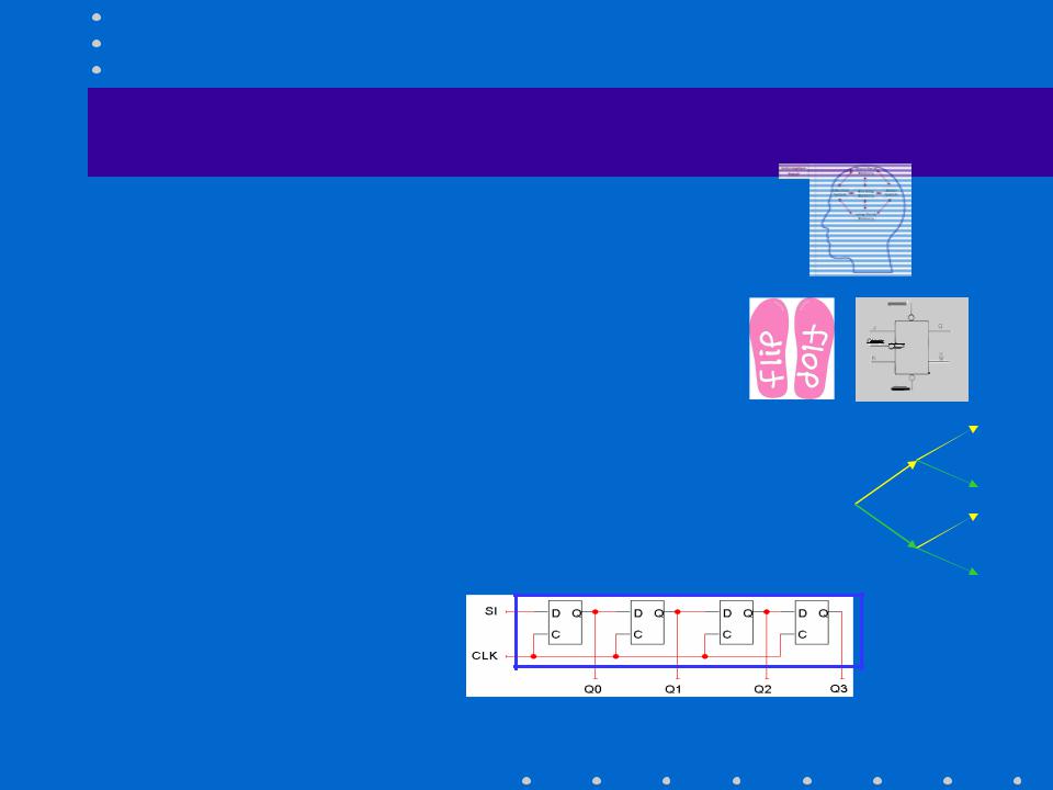
•Latch; flip-flop (D, S-R and J-K)
–a finite state machine with memory elements
•State representations
–timing
–Tree, trellis, state diagram, state table
–State table minimization
• Registers and counters
A.J. Han Vinck |
2 |
|
|
|
|
|
|
|
Introduction: the concept of memory and sequential
•What do we mean by memory?
A memory should have at least three properties.
1.It should be able to hold a value, for instance 0 or 1.
2.You should be able to read the value that was saved.
3.You should be able to change the value that’s saved.
•What do we mean by sequential circuits?
The outputs of a sequential circuit depend on not only the inputs, but also the state, or the current contents of some memory
– Examples: combination lock, elevators, traffic lights, computers, etc.
A.J. Han Vinck |
3 |
|
|
|
|
|
|
|
Types of logic: combinational
logic where the output depends on current input only
memoryless
current input
combinational
 Output
A.J. Han Vinck |
4 |
|
|
|
|
|
|
|
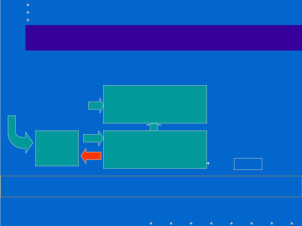
Types of logic: sequential Mealy machine
Output depends on current input and memory content
memoryless
current input
combinational
 Output
Combinational
logic
memory
memory content changes every T seconds
clock
For binary logic with n memory elements we have 2n states (different contents)
The memory contains all information about the past, necessary to account for the system‘s future behavior
A.J. Han Vinck |
5 |
|
|
|
|
|
|
|

What is next?
•We develope two basic elements with memory:
- Latch, ( Schnappriegel)
as a building block for the Flip-Flop - Flip-Flop ( a circuit with two stable states )
A.J. Han Vinck |
6 |
|
|
|
|
|
|
|
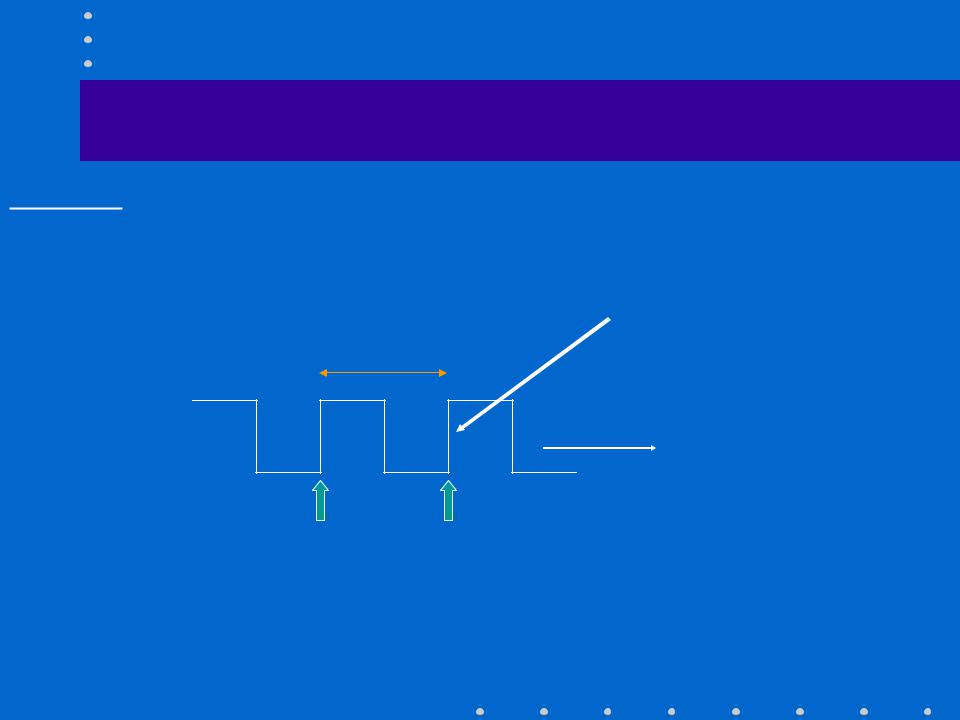
We define the clock signal
Example: Clock frequency = # of periods/second = 1 MHz (Herz)clock period 1 Sec
|
clock edge |
T |
|
1 |
|
clock |
time |
|
|
0 |
|
|
|
|
clock period: T seconds |
change state |
clock frequency: 1/T Hz |
|
|
A.J. Han Vinck |
7 |
|
|
|
|
|
|
|

2 examples of circuits with memory
1 |
0 |
Q |
|
|
s
0 |
1 |
Q‘ |
|
||
|
|
|
|
Bistable circuit |
same |
s |
1 |
(X•1)‘ = X‘ |
Q
Propagation delay in element
|
|
|
Q‘ |
A.J. Han Vinck |
1 |
8 |
|
|
|||
|
|
|
|
|
|
|
|

We use the freedom at the NAND input to change the output
R 
 Q
Q
S 
 T
T
from RS = 01 11 Q = 1 from RS = 10 11 Q = 0
this implementation is the same as used in SRAM
R |
S |
Q |
T |
|
1 |
1 |
last Q |
last T |
„state“ |
|
|
|
|
|
1 |
0 |
0 |
1 |
|
0 |
1 |
1 |
0 |
|
0 |
0 |
1 |
1 |
|
NOTE:
from RS = 00 we reach RS = 11 via 01 or 10
Both ways give a different output and thus from 00 to 11 gives unpredictable output
Note: for RS ≠ 00, T = Q‘
A.J. Han Vinck |
9 |
|
|
|
|
|
|
|

Key idea: avoid 00 as input!
force SR = 11 if output must be fixed ( use C = 0 )
For C = 1, RS = D‘D. For C = 0, RS = 11.
D |
R |
|
|
|
C.NAND.D |
C.NAND.D‘ |
|
|
|
|
|||
|
D D‘ |
C |
R |
S |
||
|
|
|||||
|
|
|
|
|
|
|
C |
|
0 |
1 |
1 |
1 |
0 |
|
|
|
|
|
|
|
|
|
1 |
0 |
1 |
0 |
1 |
|
|
0 |
1 |
0 |
1 |
1 |
|
S |
1 |
0 |
0 |
1 |
1 |
A.J. Han Vinck |
10 |
|
|
|
|
|
|
|