

dsd11-12 / dsd-11=ТКС / tks=labs / lab2_Eng_check
.pdfLABORATORY WORK No.2
STUDYING PHASE DETECTOR
Task:
1.The work is performed in the TKS library.
2.Perform the phase detector circuit simulation with XOR.
1)Create the schematic and symbol representations of the logical component NOT, performing the inverse function (Fig.1) in the Virtuoso graphics editor. Indicate pins in the following way: supply - Vdd, ground - Gnd, input - In, output - Out. The transistor dimensions should be set according to the variant in Table 1.
|
Vd |
|
|
|
|
W |
|
|
|
|
p |
|
|
|
In |
Out |
|
Vdd |
|
In |
Out |
|||
|
|
|||
|
|
|
Gnd |
W |
n |
Gn |
Fig.1 Scheme and symbol of the logical component NOT.
2)In the Virtuoso graphics editor, create the schematic and symbol representations of the logical component 2NAND, performing the function of logical multiplication with inversion (Fig.2). Indicate pins in the following way: supply - Vdd, ground - Gnd, inputs - In1 and In2, output - Out. The transistor dimensions should be set according to the variant in Table 1.
|
Vdd |
|
|
Wp |
Wp |
|
|
Lp |
Lp |
|
|
|
Out |
In1 |
Vdd |
In1А |
In2 |
Out |
|
|
Gnd |
||
|
|
|
|
In2В |
Wn |
|
|
Ln |
|
|
W n
Gnd
Fig.2 Scheme and symbol of the logical component 2NAND.
3) Create the schematic and symbol representations of the logical component XOR, performing the function AB + AB (Fig.3), in the graphics editor Virtuoso. Indicate pins in the following way: supply - Vdd, ground - Gnd, inputs - In1 and In2, output - Out.
In |
1 |
|
|
|
|
& |
|
|
|
|
|
|
|
|
|
|
|
Out |
Vdd |
|
|
& |
In1 |
|
|
|
|
In2 |
Out |
In |
1 |
& |
Gnd |
|
|
|
|
|
Fig.3 Schematic and symbolic representation of the logical component XOR.
4)Create the schematic representation of the XOR_TEST in the Virtuoso graphics editor for the transient characteristic simulation (Fig.4).
Vdd |
Vin |
In1 |
Vdd |
Out |
|
|
In2 |
Gnd |
Out |
|
|
|
||
|
|
Vin2 |
|
|
Fig. 4 Transient characteristic simulation test.
Fig. 5 shows input pulse signal diagrams. The signal parameters - the rise and decay time t=1ns, pulse period - are set according to the frequency Т=1/f

setting task variant, pulse duration is defined as ½ Т. The first pulse delay is zero. The second impulse delay is 5ns.
Vin
Vin
t=0 |
td= |
td=delay |
Fig.5. Input pulse diagrams.
5)Get the transient characteristic and the phase characteristic of the detector with the help of the additional program (Supplement 1). The second pulse delay is set parametrically td=delay.
3.Perform phase-frequency detector circuit simulation.
1)Create the schematic and symbol representations of the logical component 3NAND (Fig.1) in the graphics editor Virtuoso. Indicate pins in the following way: supply - Vdd, ground - Gnd, input - In, output - Out. The transistor dimensions are set according to the variant in Table 1.

1
V1
V3
1
V2
& |
1 |
1 |
& |
1 |
Vup |
|
&
&
&
&
& |
1 |
Vdn |
&
& |
1 |
1 |
Fig.1 Phase-frequency detector electric circuit.
Take for set Vdd=2.5V, Lmin=0.18u, W1=W2=1u, W3=W4=0.4u. Initial data variants according to the group list.
Variant |
N-MOS Width |
Frequency |
Frequency |
|
Wn, µm |
f1, MHz |
f2, MHz |
1 |
2 |
10 |
5 |
2 |
4 |
10 |
15 |
3 |
2 |
20 |
15 |
4 |
4 |
20 |
25 |
5 |
2 |
10 |
5 |
6 |
4 |
10 |
15 |
7 |
2 |
20 |
15 |
8 |
4 |
20 |
25 |
9 |
2 |
10 |
5 |
10 |
4 |
10 |
15 |
11 |
2 |
20 |
15 |
12 |
4 |
20 |
25 |
13 |
3 |
10 |
5 |
14 |
4 |
10 |
15 |
15 |
3 |
20 |
15 |
16 |
4 |
20 |
25 |
17 |
3 |
10 |
5 |
18 |
4 |
10 |
15 |
19 |
3 |
20 |
15 |
20 |
4 |
20 |
25 |
21 |
3 |
10 |
5 |
22 |
4 |
10 |
15 |
The oscillation period of this multivibrator is defined by the time of C1 capacitor recharge, the drain current Id of M5(M6) transistors operating in the current source mode:
T = 2∆t
∆t = C1 |
2 Uthres |
|
|
|||
|
Ic |
|
||||
|
|
|
|
|
||
f = |
1 |
= |
Ic |
|
||
T |
4 C U |
thres |
||||
|
|
|
|
1 |
|
|
Calculate the value of the capacitor to obtain the set frequency f0.
As the scheme is symmetric, do not forget to set the initial conditions for output voltage levels. In the Affirma Analog Environment window – Simulation – Convergence - Initial Condition voltages at the outputs are set.
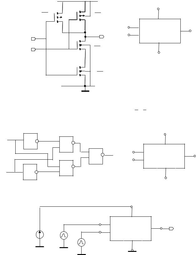
6. Perform the parametric analysis of the voltage Vvco variation. Plot the curve of the output pulse voltage frequency depending on the input voltage value (Fig.4). Define the linear range of the input voltage and the output signal frequency variation. Set the VCO transfer constant.
|
|
|
|
f |
|
|
|
|
|
|
fmax |
|
|
KVCO = |
fmax − fmin |
|
f0 |
|
||
VVCO |
−VVCO |
|
|
|
VVC |
|
|
|
max |
min |
fmin |
||
|
|
|
||||
|
|
|
|
|
||
|
|
|
|
VVCOm |
VVCOo |
VVCOm |
Fig.4. VCO transient characteristic.
7.Perform the parametric analysis of the supply voltage spread Vdd = 2V; 2.5V; 2.7V. Calculate the VCO transfer constant for each variant.
8.Perform the parametric analysis in the temperature variation range temp = -40o; 25 o ; 125 o. Calculate the VCO transfer constant for each variant.
Circuit Operation Principle.
Suppose that the M2 transistor is opened and the M1 transistor is closed. Hence a current equal IC5+IC6(equal 2IC, if М5 and М6 transistors are identical), flows through M2 and M4 transistors, as the current IC5 recharges the capacitor С1.
At the output OUT2 the voltage is equal to Vdd-2Uthres. The М3 transistor is opened, but as the current does not flow through it, there will be the Vdd-Uthres voltage at the output OUT1. The M5 drain voltage is defined by М1 and М4
transistors and is equal to Vdd-2Uthres, and the M6 drain voltage is defined by M4 and M1 transistors and varies from Vdd-Uthres to Vdd-3Uthres. Thus, the capacitor С1 discharges by 2Uthres. As soon as the M1 transistor source voltage reaches Vdd3Uthres, it opens and the М2 transistor closes. Now the M6 transistor drain current will charge the capacitor C1 with the current IC6. As the transistor dynamic
parameters are good, the switching is fast. The output voltages will change, there
will be Vdd-2Uthres at the output OUT1, and Vdd-Uthres at the output OUT2. The voltages at the capacitor plates will be: Vdd-2Uthres at the M5 drain and Vdd-Uthres at the М6 drain. The timing sheets are shown in Fig. 5.
Final report contents.
1.Preliminary calculating the value of Capacity C1.
2.Printing out the multivibrator circuit.
3.Printing out the test circuit.
4.VCO transfer characteristic diagram.
5.Defining the VCO transfer constant.
6.The VCO frequency versus the supply voltage spread curve. Defining the VCO transfer constant.
7.The VCO frequency versus the temperature spread curve. Defining the VCO transfer constant.
8.Printing out the timing sheets for the nominal supply and the normal temperature when the voltage is Vvco0
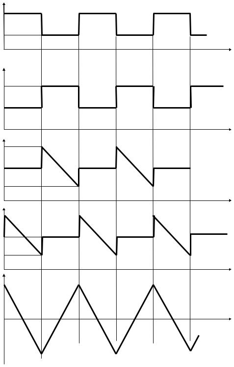
UOUT1
Vdd-Uthres
Vdd-2Uthres
UOUT2
Vdd-Uthres
Vdd-2Uthres
UИ2
Vdd-Uthres
Vdd-2Uthres
Vdd-3Uthres
UИ1
Vdd-Uthres
Vdd-2Uthres
Vdd-3Uthres
UС1
Uthres
-Uthres
Fig.4. VCO voltage timing sheets.
t
t
t
t
t