
Davis W.A.Radio frequency circuit design.2001
.pdf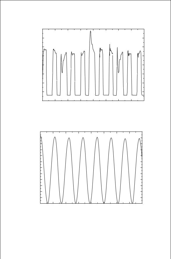
190
Collector Voltage
RF POWER AMPLIFIERS
50.00 |
|
|
|
|
|
|
|
|
40.00 |
|
|
|
|
|
|
|
|
30.00 |
|
|
|
|
|
|
|
|
20.00 |
|
|
|
|
|
|
|
|
10.00 |
|
|
|
|
|
|
|
|
0.00 |
|
|
|
|
|
|
|
|
–10.00 |
|
|
|
|
|
|
|
|
– 20.00 |
|
|
|
|
|
|
|
|
– 30.00 |
70.5 |
71.0 |
71.5 |
72.0 |
72.5 |
73.0 |
73.5 |
74.0 |
70.0 |
Time, ns
FIGURE 9.18 Class F collector voltage when the ac VG D 0.11 volts.
Power, W
12.00 |
|
|
|
|
|
|
|
|
11.00 |
|
|
|
|
|
|
|
|
10.00 |
|
|
|
|
|
|
|
|
9.00 |
|
|
|
|
|
|
|
|
8.00 |
|
|
|
|
|
|
|
|
7.00 |
|
|
|
|
|
|
|
|
6.00 |
|
|
|
|
|
|
|
|
5.00 |
|
|
|
|
|
|
|
|
4.00 |
|
|
|
|
|
|
|
|
3.00 |
|
|
|
|
|
|
|
|
2.00 |
|
|
|
|
|
|
|
|
1.00 |
|
|
|
|
|
|
|
|
0.00 |
70.5 |
71.0 |
71.5 |
72.0 |
72.5 |
73.0 |
73.5 |
74.0 |
70.0 |
Time, ns
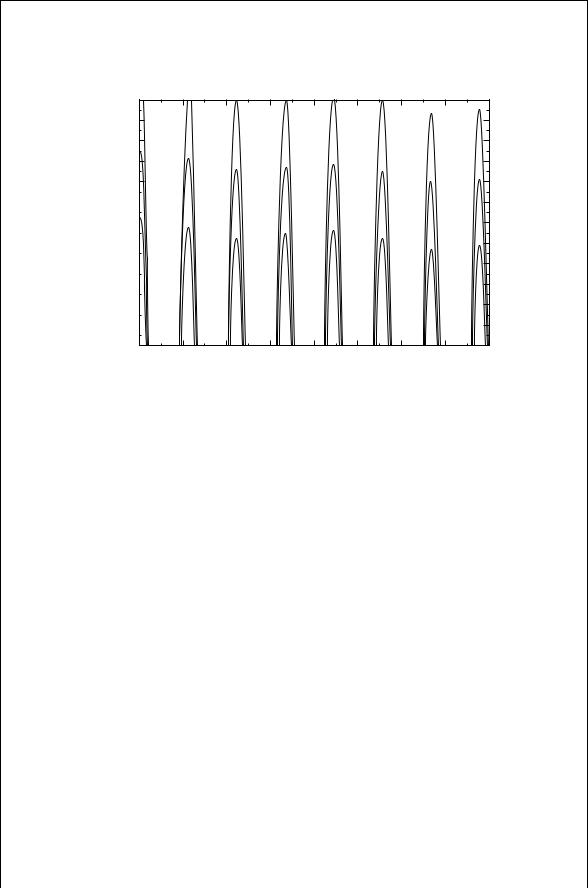
FIGURE 9.19 Class F collector load power when the ac VG D 0.11 volts.
11.00
10.75
10.50
10.25
10.00
W |
9.75 |
|
|
|
|
||
Power, |
9.50 |
|
|
|
|
|
|
|
9.25 |
|
|
|
|
|
|
|
9.00 |
|
|
|
|
|
|
|
8.75 |
|
|
|
|
|
|
|
8.50 |
|
|
|
|
|
|
|
8.25 |
|
|
|
|
|
|
|
8.00 |
|
|
|
70.0 |
||
FEED-FORWARD AMPLIFIERS |
191 |
VG = 0.11
0.09
0.15
70.5 |
71.0 |
71.5 |
72.0 |
72.5 |
73.0 |
73.5 |
74.0 |
Time, ns
FIGURE 9.20 Class F collector load power as a function of VG.
The bad news is that the output power is very sensitive to the amplitude of the ac input voltage, VG, as demonstrated in Fig. 9.20. A more extensive harmonic balance analysis of a physics based model for a metal semiconductor field effect transistor (MESFET) showed that a power added efficiency of 75% can be achieved at 5 GHz [6].
9.7FEED-FORWARD AMPLIFIERS
The concept of feed-forward error control was conceived in a patent disclosure by Harold S. Black in 1924 [7]. This was several years prior to his more famous concept of feedback error control. An historical perspective on the feed-forward idea is found in [8]. The feedback approach is an attempt to correct an error after it has occurred. A 180° phase difference in the forward and reverse paths in a feedback system can cause unwanted oscillations. In contrast, the feed-forward design is based on cancellation of amplifier errors in the same time frame in which they occur. Signals are handled by wideband analog circuits, so multiple carriers in a signal can be controlled simultaneously. Feed-forward amplifiers are inherently stable, but this comes at the price of a somewhat more complicated circuit. Consequently feed-forward circuitry is sensitive to changes in ambient temperature, input power level, and supply voltage variation. Nevertheless, feedforward offers many advantages that have brought it increased interest.
The major source of distortion, such as harmonics, intermodulation distortion, and noise, in a transmitter is the power amplifier. This distortion can be greatly
192 |
RF POWER AMPLIFIERS |
|
|
|
|
|
coup1 |
Main Amp |
coup2 |
delay2 |
coup4 |
−C 1 dB |
G 1 dB |
−C 2 dB |
−D 2 dB |
−C 4 dB |
|
|
|
|
−L 1 |
dB |
|
|
delay1 |
−C 3 dB |
Error Amp |
||
|
|
|
|
||
|
−D 1 |
dB |
coup3 |
G 2 |
dB |
|
|
|
|
||
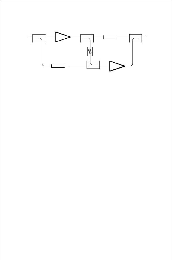
FIGURE 9.21 Linear feed-forward amplifier.
reduced using feed-forward design. The basic idea is illustrated in Fig. 9.21, where it is seen that the circuit consists basically of two loops. The first one contains the main power amplifier, and the second loop contains the error amplifier. In the first loop, a sample of the input signal is coupled through “coup1” reducing the signal by the coupling factor C1 dB. This goes through the delay line with insertion loss of D1 dB into the comparator coupler “coup3.” At the same time the signal passing through the main amplifier with gain G1 dB is sampled by coupler “coup2” reducing the signal by C2 dB, the attenuator by L1 dB, and the coupler “coup3” by C3 dB. The delay line is adjusted to compensate for the time delay in the main amplifier as well as the passive components so that two input signals for “coup3” are 180° out of phase but synchronized in time. The amplitude of the input signal when it arrives at the error amplifier is
C1 D1 [G1 C2 L1 C3] |
9.71 |
which should be adjusted to be zero. What remains is the distortion and noise added by the main amplifier which is in turn amplified by the error amplifier by G2 dB. At the same time the signal from the main amplifier with its distortion and noise is attenuated by D2 dB in the second loop delay line. The second delay line is adjusted to compensate for the time delay in the error amplifier. The relative phase and amplitude of the input signals to “coup4” are adjusted so that the distortion terms cancel. The output distortion amplitude
D2 [ C2 L1 C3 C G2 C4] |
9.72 |
should be zero for complete cancellation to occur.
The error amplifier will also add distortion and noise to its input signal so that perfect error correction will not occur. Nevertheless, a dramatic improvement is possible, since the error amplifier will be operating on a smaller signal (only distortion) that will likely lie in the linear range of the amplifier. Further improvement may be accomplished by treating the entire amplifier in Fig. 9.21 as the main amplifier and adding another error amplifier with its associated circuitry [8].

REFERENCES 193
A typical implementation of a feed-forward system is described in [9] for an amplifier operating in the frequency range of 2.1 to 2.3 GHz with an RF gain of 30 dB, and an output power of 1.25 W. This amplifier had intermodulation products at least 50 dB below the carrier level. Their design used a 6 dB coupler for “coup1,” a 13 dB coupler for “coup2,” a 10 dB coupler for “coup3,” and an 8 dB coupler for “coup4.” In some designs the comparator coupler, “coup3,” is replaced by a power combiner.
The directional coupler itself can be implemented using microstrip or stripline coupled lines at higher frequencies [10] or by a transmission line transformer. A variety of feed forward designs have been implemented, some using digital techniques [11,12].
PROBLEMS
9.1If the crossover discontinuity is neglected, is a class B amplifier considered a linear amplifier or a nonlinear amplifier? Explain your answer.
9.2A class B amplifier such as that shown in Fig. 9.7 is biased with an 18 volt power supply, but the maximum voltage amplitude across each transistor is 16 volts. The remaining 2 volts is dissipated as loss in the output transformer. If the amplifier is designed to deliver 12 W of RF power, find the following:
(a)The maximum RF collector current
(b)The total dc current from the power supply
(c)The collector efficiency of this amplifier.
9.3The class C amplifier shown in Fig. 9.9 has a conduction angle of 60°. It is designed to deliver 75 W of RF output power. The saturated collector–emitter voltage is known to be 1 volt, and the power supply voltage is 26 volts. What is the maximum peak collector current.
REFERENCES
1.P. R. Gray and R. G. Meyer, Analysis and Design of Analog Integrated Circuits, New York: Wiley, 1993.
2.H. L. Krauss, C. W. Bostian, and F. H. Raab, Solid State Radio Engineering, New York: Wiley, 1980.
3.D. M. Snider, “A Theoretical Analysis and Experimental Confirmation of the Optimally Loaded and Overdriven RF Power Amplifier,” IEEE Trans. on Electron Devices, Vol. ED-14, pp. 851–857, 1967.
4.F. H. Raab, “Class-F Power Amplifiers with Maximally Flat Waveforms,” IEEE Trans. Microwave Theory Tech., Vol. 45, pp. 2007–2012, 1997.
5.C. Trask, “Class-F Amplifier Loading Networks: A Unified Design Approach,” 1999 IEEE MTT-S International Symp. Digest, Piscataway, NJ: IEEE Press, 1999, pp. 351– 354.

194 RF POWER AMPLIFIERS
6.L. C. Hall and R. J. Trew, “Maximum Efficiency Tuning of Microwave Amplifiers,” 1991 MTT-S International Symp. Digest, Piscataway, NJ: IEEE Press, 1991, pp. 123– 126.
7.H. S. Black, U.S. Patent 1,686,792, issued October 9, 1929.
8.H. Seidel, H. R. Beurrier, and A. N. Friedman, “Error-Controlled High Power Linear Amplifiers at VHF,” Bell Sys. Tech. J., Vol. 47, pp. 651–722, 1968.
9.C. Hsieh and S. Chan, “A Feedforward S-Band MIC Amplifier System,” IEEE J. Solid State Circuits, Vol. SC-11, pp. 271–278, 1976.
10.W. A. Davis Microwave Semiconductor Circuit Design, 1984, Ch. 4.
11.S. J. Grant, J. K. Cavers, and P. A. Goud, “A DSP Controlled Adaptive Feed Forward Amplifier Linearizer,” Annual International Conference on Universal Personal Communications, pp. 788–792, September 29–October 2, 1996.
12.G. Zhao, F. M. Channouchi, F. Beauregard, and A. B. Kouki, “Digital Implementations of Adaptive Feedforward Amplifier Linearization Techniques,” IEEE Microwave Theory Tech. Symp. Digest, June 1996.


TWO-PORT OSCILLATORS WITH EXTERNAL FEEDBACK |
197 |
when jaˇj D 1 and 6aˇ D 360°. An alternate way of determining conditions for oscillation is determining when the value k < 1 for the stability circle as described in Chapter 7. Still a third way will be considered later in Section 10.4.
10.2FEEDBACK THEORY
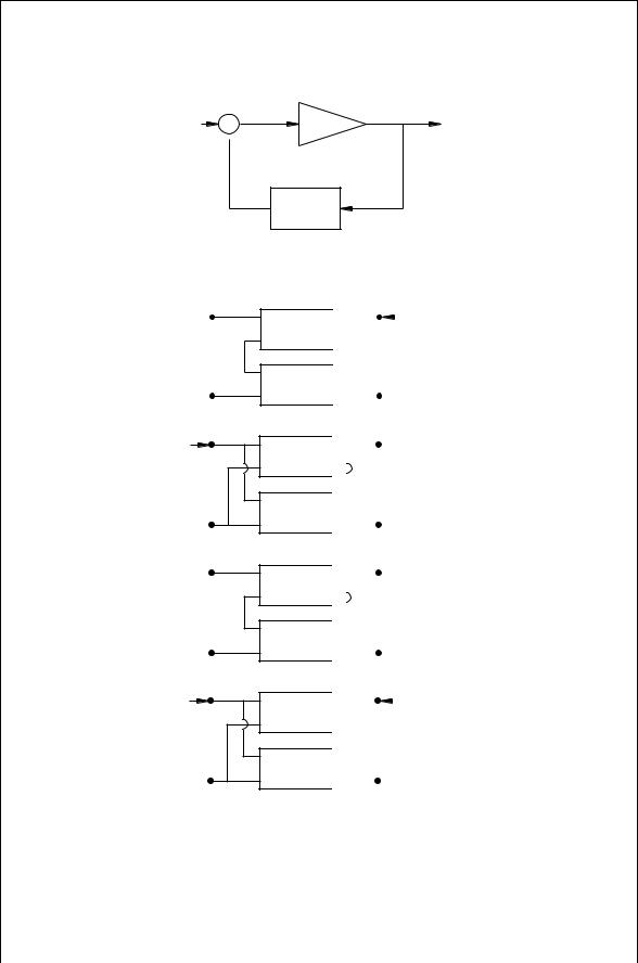
The active amplifier part and the passive feedback part of the oscillator can be considered as a pair of two two-port circuits. Usually the connection of these two-ports occurs in four different ways: series–series, shunt–shunt, series–shunt, and shunt–series (Fig. 10.2). A linear analysis of the combination of these two two-ports begins by determining what type of connection exists between them. If, for example, they are connected in series–series, then the best way to describe each of the two-ports is in terms of their z parameters. A description of the composite of the two two-ports is found by simply adding the z parameters of the two circuits together. Thus, if [za] and [zf] represent the amplifier and feedback circuits connected in series–series, then the composite circuit is described by [zc] D [za] C [zf]. The form of the feedback circuit itself can take a wide range of forms, but being a linear circuit, it can always be reduced to a set of z, y, h or g parameters, any one of which can be represented by k for the present. The term that feeds back to the input of the amplifier is k12f. The k12f term, though small, is a significant part of the small incoming signal, so it cannot be neglected. The open loop gain, a, of the composite circuit is found by setting k12f D 0. Then, using the normal circuit analysis, the open loop gain is determined. The closed loop gain is found by including k12f in the closed loop gain given by Eq. (10.1). The Barkhausen criterion for oscillation is satisfied when ak12f D aˇ D 1.
10.3TWO-PORT OSCILLATORS WITH EXTERNAL FEEDBACK
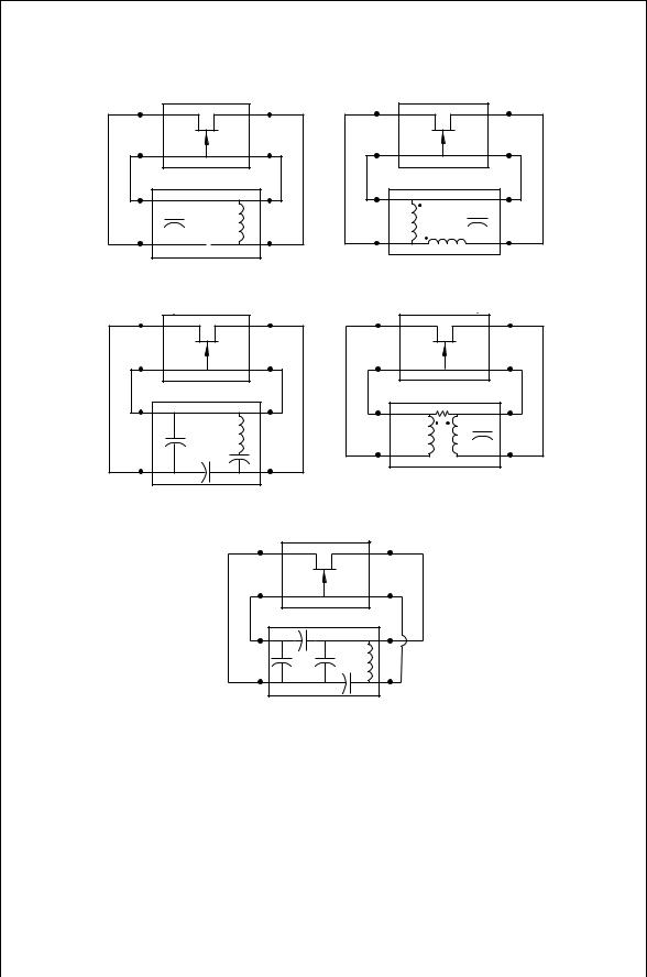
There are a wide variety of two-port oscillator circuits that can be designed. The variety of oscillators results from the different ways the feedback circuit is connected to the amplifier and the variety of feedback circuits themselves. Five of these shown in Fig. 10.3 are known as the Colpitts, Hartley, ClappGouriet [1,2], Armstrong, and Vackar [2,3] oscillators. The Pierce oscillator is obtained by replacing the inductor in the Colpitts circuit with a crystal that acts like a high Q inductor. As shown the first four of these feedback circuits are drawn in a series–series connection, while the Vackar is drawn as a series–shunt configuration. Of course a wide variety of connections and feedback circuits are possible. In each of these oscillators, there is a relatively large amount of energy stored in the resonant reactive circuit. If not too much is dissipated in the load, sustained oscillations are possible.
The Colpitts is generally favored over that of the Hartley, because the Colpitts circuit capacitors usually have higher Q than inductors at RF frequencies and come in a wider selection of types and sizes. In addition the inductances in the Hartley circuit can provide a means to generate spurious frequencies because it
TWO-PORT OSCILLATORS WITH EXTERNAL FEEDBACK |
199 |
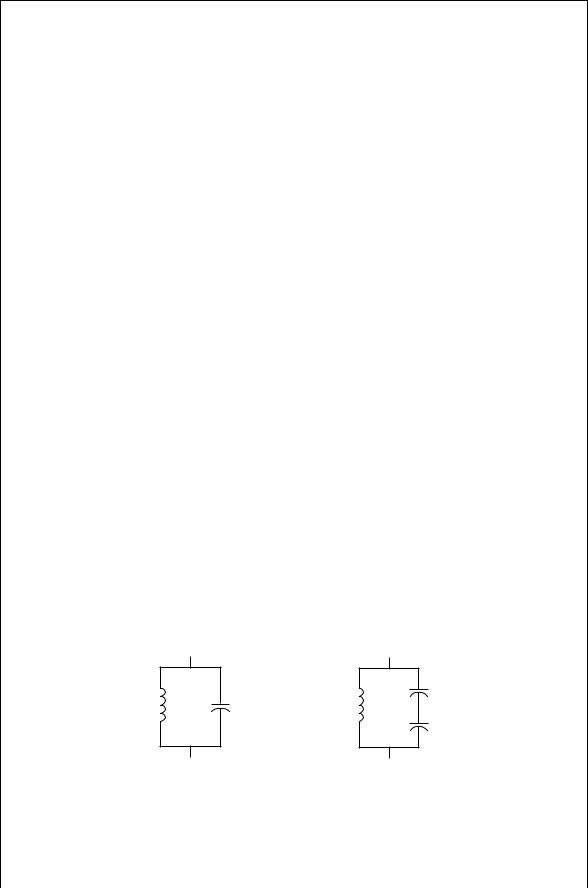
In a voltage-controlled oscillator application, it is often convenient to vary the capacitance to change the frequency. This can be done using a reverse biased varactor diode as the capacitor. If the capacitance shown in Fig. 10.4a changes because of say a temperature shift, the frequency will change by
df |
dC0 |
10.3 |
|
|
D |
|
|
|
|
||
f2C0
However, the tapped circuit in Fig. 10.4b in which C2 is used for tuning a Colpitts circuit has a frequency stability given by
df |
D |
C0 |
|
dC2 |
10.4 |
|
f |
C2 C2 |
|||||
|
|
|||||
This has an improved stability by the factor of C0/C2. Furthermore, by increasing C0 so that C1 and C2 are increased by even more while adjusting the inductance to maintain the same resonant frequency, the stability can be further enhanced. The Clapp-Gouriet circuit exhibits even better stability than the Colpitts [2]. In this circuit, C1 and C2 are chosen to have large values compared to the tuning capacitor C3. The minimum transistor transconductance, gm, required for oscillation for the Clapp-Gouriet circuit increases / ω3/Q. While the Q of a circuit often rises with frequency, it would not be sufficient to overcome the cubic change in frequency. For the Vackar circuit, the required minimum gm to maintain oscillation is / ω/Q. This would tend to provide a slow drop in the amplitude of the oscillations as the frequency rises [2].
The oscillator is clearly a nonlinear circuit, but nonlinear circuits are difficult to treat analytically. In the interest of trying to get a design solution, linear analysis is used. It can be said that a circuit can be treated by small signal linear mathematics to just prior to it’s breaking into oscillation. In going through the transition between oscillation and linear gain, the active part of the circuit does not change appreciably. As a justification for using linear analysis, the previous statement certainly has some flaws. Nevertheless, linear analysis does give remarkably close answers. More advanced computer modeling using methods like harmonic balance will give more accurate results and provide predictions of output power.
L |
|
C2 |
C0 |
L |
|
|
|
C1 |
|
(a ) |
(b ) |
FIGURE 10.4 (a) Simple LC resonant circuit and (b) tapped capacitor LC circuit used in the Colpitts oscillator.

 +
+