

Davis W.A.Radio frequency circuit design.2001
.pdf
TWO-PORT OSCILLATORS WITH EXTERNAL FEEDBACK |
201 |
The open loop gain, a, for the shunt–shunt configuration is
a |
|
vo |
|
vo |
|
gm C y12f |
10.9 |
|
D ii |
D vgsy11f |
D y11f[ 1/RD C y22f] |
||||||
|
|
|||||||
The negative sign introduced in getting ii is needed to make the current go north rather than south as made necessary by the usual sign convention. Finally, by the Barkhausen criterion, oscillation occurs when ˇa D 1:
1 |
D |
ay |
|
y12f gm C y12f |
10.10 |
|
12f D y11f[ 1/RD C y22f] |
||||||
|
|
|
||||
Making the appropriate substitutions from Eqs. (10.5) through (10.7) results in the following:
1 |
|
1 |
1 |
|
1 |
1 |
10.11 |
|||||
gm |
|
D sL |
sC1 C |
|
|
|
C |
sC1 C |
|
sC2 C |
|
|
sL |
sL |
RD |
sL |
sL |
||||||||
Both the real and imaginary parts of this equation must be equal on both sides. Since s D jω0 at the oscillation frequency, all even powers of s are real and all odd powers of s are imaginary. Since gm in Eq. (10.11) is associated with the real part of the equation, the imaginary part should be considered first:
1 |
D sL s2C1C2 C |
C1 |
|
C2 |
1 |
10.12 |
|
|
|
C |
|
C |
|
||
sL |
L |
L |
s2L2 |
||||
When this is solved, the oscillation frequency is found to be
ω |
D |
C1 C C2 |
10.13 |
|
LC1C2 |
||||
0 |
|
Solving the real part of Eq. (10.11) with the now known value for ω0 gives the required value for gm:
C1 |
10.14 |
gm D RDC2 |
The value for gm found in Eq. (10.14) is the minimum transconductance the transistor must have in order to produce oscillations. The small signal analysis is sufficient to determine conditions for oscillation assuming the frequency of oscillation does not change with current amplitude in the active device. The large signal nonlinear analysis would be required to determine the precise frequency of oscillation, the output power, the harmonic content of the oscillation, and the conditions for minimum noise.

|
|
|
PRACTICAL OSCILLATOR EXAMPLE |
203 |
|
frequency of oscillation and minimum transconductance can be found: |
|
||||
1 |
|
10.17 |
|||
ω0 D |
p |
|
|
|
|
C L1 C L2 |
|
||||
gm D |
L2 |
10.18 |
|||
L1R |
|
||||
For a 10 MHz oscillator biased with VDD D 15 V, the inductances, L1 and L2 are chosen to be both equal to 1 H. The capacitance from Eq. (10.17) is 126.6 pF. If the minimum device transconductance for a 2N3819 JFET is 3.5 mS, then from Eq. (10.18), R > 285 . Choosing the resistance R to be 300 will require the transformer turns ratio to be
|
n2 |
D |
R |
D 2.45 |
|
|
|
||
|
n3 |
RL |
|
|
|
||||
and |
|
|
|
|
|
|
|
|
|
|
|
|
|
n3 |
2 |
|
1 |
2 |
|
|
L3 D L2 |
|
D |
1 Ð |
D 0.1667 !H |
||||
|
|
|
|
||||||
|
|
n2 |
2.45 |
||||||
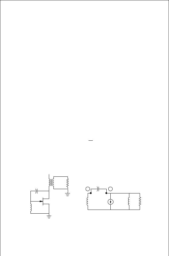
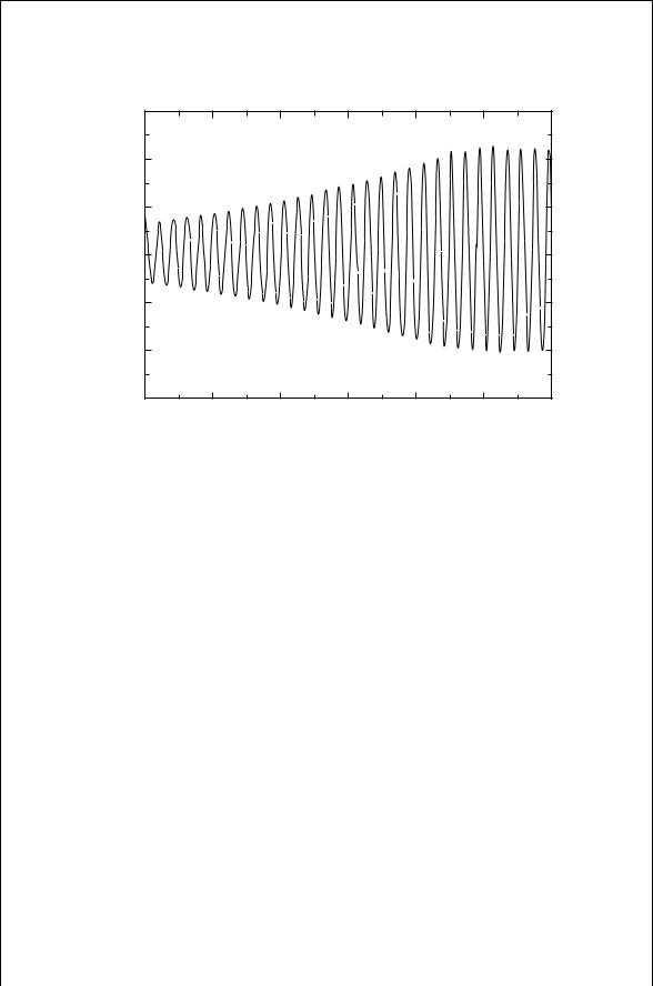
These circuit values can be put into SPICE to check for the oscillation. However, SPICE will give zero output when there is zero input. Somehow a transient must be used to start the circuit oscillating. If the circuit is designed correctly, oscillations will be self-sustaining after the initial transient. One way to initiate a start up transient is to prevent SPICE from setting up the dc bias voltages prior to doing a time domain analysis. This is done by using the SKIPBP (skip bias point) or UIC (use initial conditions) command in the transient statement. In addition it may be helpful to impose an initial voltage condition on a capacitance or initial current condition on an inductance. A second approach is to use the PWL (piecewise linear) transient voltage somewhere in the circuit to impose a short pulse at t D 0 which forever after is turned off. The first approach is illustrated in the SPICE net list for the Hartley oscillator.
Hartley |
Oscillator Example. 10 MHz, RL = 50. |
||||
* This will |
take some time. |
||||
L1 |
1 |
16 |
1u |
|
|
VDC |
16 |
0 |
DC |
-1.5 |
|
C |
1 |
2 |
126.7p |
IC=-15 |
|
L2 |
3 |
2 |
1u |
|
|
L3 |
4 |
0 |
.1667u |
|
|
K23 |
L2 |
L3 |
.9999 |
;Unity coupling not allowed |
|
RL |
4 |
0 |
50. |
|
|
J1 |
2 |
1 |
0 |
J2N3819 |
|
.LIB |
EVAL.LIB |
|
|
|
|
VDD |
3 |
0 |
15 |
|
|


206 OSCILLATORS AND HARMONIC GENERATORS
Thus Eqs. (10.21) and (10.24) are equivalent conditions for oscillation. In any case, the stability factor, k, for the composite circuit with feedback must be less than one to make the circuit unstable and thus capable of oscillation.
An equivalent condition for the load port may be found from Eq. (10.24). From Eq. (7.17) in Chapter 7, the input reflection coefficient for a terminated two-port was found to be
i D S11 C |
S12S21 L |
|
|||||
1 S22 L |
|
|
|||||
|
S11 L |
|
1 |
10.25 |
|||
D |
1 S22 L |
D G |
|||||
|
|||||||
where is the determinate of the S-parameter matrix. Solving the right-hand side of Eq. (10.25) for L gives
|
|
1 S11 G |
|
|
|
10.26 |
||
|
|
|
|
|
|
|
||
L D S12 G |
|
|
|
|
||||
But from Eq. (7.21), |
|
|
|
|
|
|
|
|
o D S22 C |
S12S21 G |
|
||||||
1 S11 G |
|
|
||||||
|
S22 G |
|
|
1 |
10.27 |
|||
D |
1 S11 G D |
|
L |
|||||
|
|
|||||||
The last equality results from Eq. (10.26). The implication is that if the conditions for oscillation exists at one port, they also necessarily exist at the other port.
10.6COMMON GATE (BASE) OSCILLATORS
A common gate configuration is often advantageous for oscillators because they have a large intrinsic reverse gain (S12g) that provides the necessary feedback. Furthermore feedback can be enhanced by putting some inductance between the gate and ground. Common gate oscillators often have low spectral purity but wide band tunability. Consequently they are often preferred in voltage-controlled oscillator (VCO) designs. For a small signal approximate calculation, the scattering parameters of the transistor are typically found from measurements at a variety of bias current levels. Probably the S parameters associated with the largest output power as an amplifier would be those to be chosen for oscillator design. Since common source S parameters, Sij, are usually given, it is necessary to convert them to common gate S parameters, Sijg. Once this is done, the revised S parameters may be used in a direct fashion to check for conditions of oscillation.

COMMON GATE (BASE) OSCILLATORS 207
The objective at this point is to determine the common gate S parameters with the possibility of having added gate inductance. These are derived from the common source S parameters. The procedure follows:
1.Convert the two-port common source S parameters to two-port common source y parameters.
2.Convert the two-port y parameters to three-port indefinite y parameters.
3.Convert the three-port y parameters to three-port S parameters.
4.One of the three-port terminals is terminated with a load of known reflection coefficient, r.
5.With one port terminated, the S parameters are converted to two-port S parameters, which could be, among other things, common gate S parameters.
At first, one might be tempted to convert the 3 ð 3 indefinite admittance matrix to a common gate admittance matrix and convert that to S parameters. The problem is that “common gate” usually means shorting the gate to ground, which is fine for y parameters, but it is not the same as terminating the gate with a matched load or other impedance, Zg, for the S parameters.
The first step, converting the S parameters to y parameters, can be done using the formulas in Table D.1 or Eq. (D.10) in Appendix D. For example, if the common source S parameters, [Ss], are given the y parameter matrix is
|
1 S11s 1 C S22s C S12sS21s |
|
|
2S12s |
|
||||
[Ys] D Y0 |
|
Ds |
|
|
Ds |
||||
|
2S21s |
|
|
1 C S11s 1 S22s C S12sS21s |
|
||||
|
|
|
|
||||||
|
|
|
Ds |
|
|
Ds |
|||
|
|
|
|
|
10.28 |
||||
where |
|
|
|
|
|
|
|
|
|
|
1 C S22s S12sS21s |
10.29 |
|||||||
Ds D 1 C S11s |
|||||||||
Next the y parameters are converted to the 3 ð 3 indefinite admittance matrix. The term “indefinite” implies that there is no assumed reference terminal for the circuit described by this matrix [5]. The indefinite matrix is easily found from its property that the sum of the rows of the matrix is zero, and the sum of the columns is zero. Purely for convenience, this third row and column will be added to the center of the matrix. Then the y11 will represent the gate admittance, the y22 the source admittance, and the y33 the drain admittance. The new elements for the indefinite matrix are then put in between the first and second rows and in between the first and second columns of Eq. (10.28). For example, the new y12 is
y |
12 |
D |
Y |
0 |
2S12s 1 S11s 1 C S22s C S12sS21s S12sS21s |
10.30 |
|
Ds |
|||||||
|
|
|


|
COMMON GATE (BASE) OSCILLATORS |
209 |
||
r |
Zi Zref |
|
10.35 |
|
Zi C Zref |
||||
i D |
|
|||
The reflection coefficient is determined relative to the reference impedance which is the impedance looking back into to the transistor. With Eq. (10.34), b2 can be eliminated in Eq. (10.33) giving a relationship between a1 and a2:
|
a2 |
|
|
|
|
||||
|
|
|
D S21a1 |
C S22a2 |
|
||||
|
rs |
|
|||||||
|
a2 D |
S21a1 |
|
|
10.36 |
||||
|
1/rs S22 |
|
|||||||
The ratio between b1 and a1 under these conditions is |
|
||||||||
S11s D |
b1 |
|
S12S21 |
10.37 |
|||||
|
D S11 |
C |
|
||||||
a1 |
1/rs S22 |
||||||||
This represents the revised S11s scattering parameter when the source is terminated with an impedance whose reflection coefficient is rs. In similar fashion the other parameters can be easily found, as shown in Appendix E. The numbering system for the common source parameters is set up so that the input port (gate side) is port-1 and the output port (drain) is port-2. Therefore the subscripts of the common source parameters, Sijs, range from 1 to 2. In other words, after the source is terminated, there are only two ports, the input and output. These are written in terms of the three-port scattering parameters, Sij, which of course have subscripts that range from 1 to 3.
The common gate connection can be calculated using this procedure. The explicit formulas are given in Appendix E. For a particular RF transistor, in which the generator is terminated with a 5 nH inductor, the required load impedance on the drain side to make the circuit oscillate is shown in Fig. 10.11 as obtained from the program SPARC (S-parameters conversion). Since a passive resistance must be positive, the circuit is capable of oscillation only for those frequencies in which the resistance is above the 0 line. An actual oscillator would still require a resonator to force the oscillator to provide power at a single frequency. A numerical calculation at 2 GHz that illustrates the process is found in Appendix E.
When the real part of the load impedance is less than the negative of the real part of the device impedance, then oscillations will occur at the frequency where there is resonance between the load and the device. For a one-port oscillator, the negative resistance is a result of feedback, but here the feedback is produced by the device itself rather than by an external path. Specific examples of one-port oscillators use a Gunn or IMPATT diode as the active device. These are normally used at frequencies above the band of interest here. On the surface the one-port oscillator is in principle no different than a two-port oscillator whose opposite side is terminated in something that will produce negative resistance at the other end. The negative resistance in the device compensates for positive resistance in the