Добавил:
Опубликованный материал нарушает ваши авторские права? Сообщите нам.
Вуз: Предмет: Файл:

Davis W.A.Radio frequency circuit design.2001

.pdf
Скачиваний:
94
Добавлен:
23.08.2013
Размер:
2.47 Mб
Скачать

250 PHASE LOCK LOOPS

Frequency is the time rate of change of phase, so phase is the time integral of frequency. Consequently, if the frequency of the VCO is proportional to the tuning voltage, the output phase is proportional to the integral of tuning voltage. The output frequency can range from a few Hertz to many GHz. The VCO output becomes the second input to the phase detector.

When the loop is first turned on, the VCO frequency is not controlled. The loop filter output voltage can be anywhere between the high and low limits set by the power supply. However, the phase detector produces an error voltage that is the difference between the VCO frequency and the reference frequency. Like the cruise control example, this signal tells the loop filter whether the VCO is going too fast or too slow relative to the reference frequency. The loop filter is “smart enough” to know what to do. If the error signal indicates that the VCO frequency is less than the reference, the loop filter adjusts the control voltage to raise the VCO frequency. If the VCO frequency is too high, the loop filter changes the voltage and lowers the VCO frequency. The loop filter design sets how fast this happens. Some loops may be designed for a fast bumpy ride, while others may require a slow smooth ride. When the loop filter has done its job, the VCO frequency will exactly match the reference frequency, and the two inputs will have a constant phase difference. This match in frequency and constant phase difference will be maintained even if the reference frequency changes. With each change, the PLL again goes through the settling out process. If the reference is noisy, the PLL is in a continual state of change, working hard to follow the input. If a PLL were nothing more than a box with the same frequency in and out, it would not be much of an invention. Happily there is a lot more to it than that. Before preceding any farther, the basic idea of the frequency control by a closed loop operation must be clarified.

12.5LOOP DESIGN PRINCIPLES

There are many design rules that go into a successful, stable closed loop design, but many of these details are beyond the scope of his text. However, this discussion will lead to an understanding of how the loop works and how to select parts to customize its operation. From the overall system point of view, the PLL designer must know the overall requirements and be able to translate these requirements into the PLL parameters for the design.

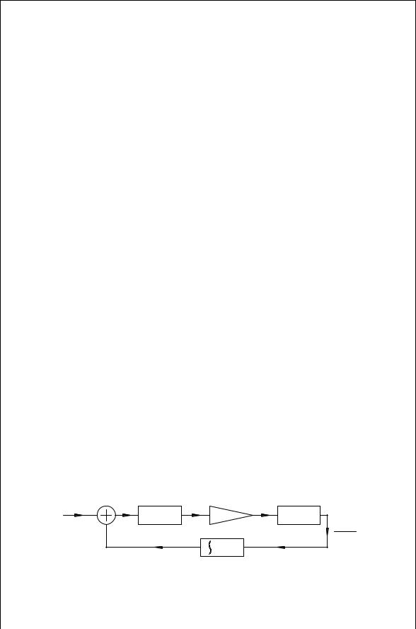
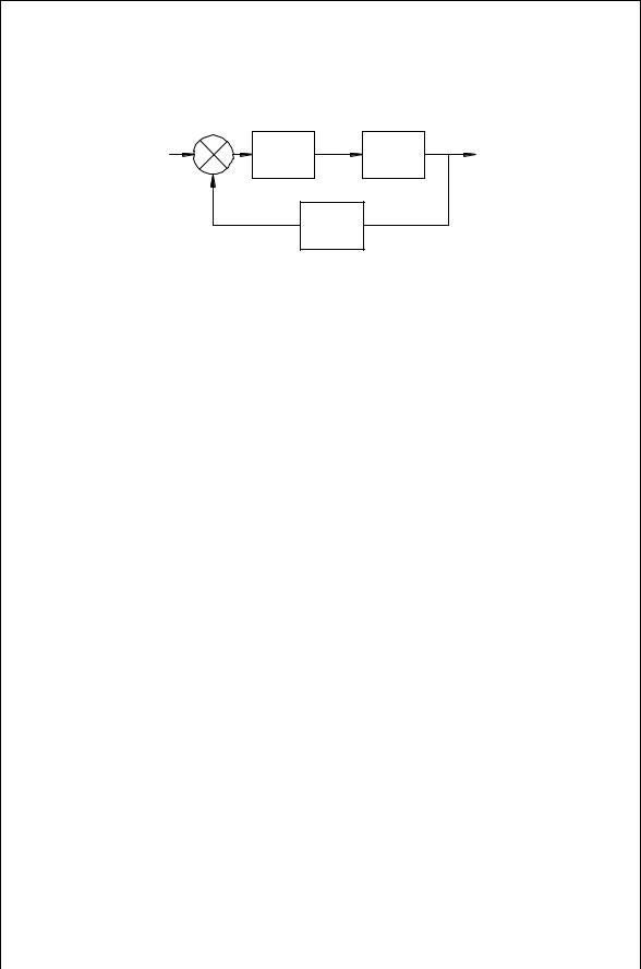
With a PLL, the important top-level parameters are the input and output frequency, the response time, the loop bandwidth and the loop damping ratio. The top-level view concentrates on these system level values. The detailed aspects of the phase detector and VCO must be considered. These are usually highfrequency parts requiring high-frequency design techniques. The design of the loop filter requires an understanding of analog design techniques. Figure 12.2 illustrates the PLL block diagram, which includes a frequency divider in the feedback path. Both frequencies coming into the phase detector must be the locked together at the same frequency. This will force the output frequency,


PLL COMPONENTS

251


Phase


Detector


fref

Loop

VCO

fout


Filter


Divide

by N

FIGURE 12.2 Phase lock loop with a frequency divider.

fout, to be N times the reference frequency, fref. Familiarity with digital circuit design is required to complete the design. A PLL design is not just a system design nor an RF design nor an analog design, but it is a combination of all these areas. The actual design process can be summarized by three principles.

1.Know each component. The components of a PLL, the VCO, phase detector, loop filter, and frequency divider must be thoroughly understood and tested as stand-alone individual components. Testing of the actual parts must show that they each meet the design goals. These tests may extend far beyond the information on the manufacturer’s data sheet.

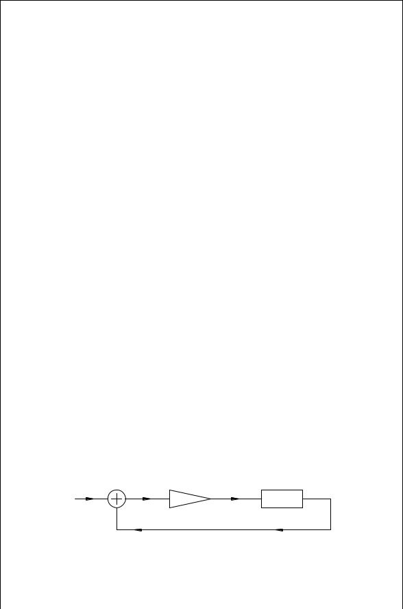
2.Test the components together. The individual components must work correctly when connected together in an open loop configuration. The loop filter must put out enough voltage to drive the VCO. The VCO must have enough output to drive the frequency divider. The phase detector output must be large enough for the loop filter to use. An open loop analysis must show the correct phase margin and bandwidth for stability. These issues are resolved with an open loop analysis.

3.Compare the closed loop configuration to the design goals. A closed loop analysis should show that the final connection matches the system level design goals. Both test measurement techniques and analysis can be applied for PLL design verification.

12.6PLL COMPONENTS

The basic building blocks, except in exotic applications, are those shown in Fig. 12.2. This section describes in greater depth each of these functions.

12.6.1Phase Detectors

Phase detectors come in many configurations. These include those with logic level inputs, passive and active analog versions, and sampling versions used for highfrequency multiplication. In addition there are phase detectors with automatic

252 PHASE LOCK LOOPS

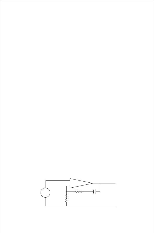
frequency search features to aid in initial frequency acquisition. In its simplest form, a phase detector is a frequency mixer. As described in Chapter 11, when two signals come into the mixer, the output consists primarily in the sum and difference frequencies. The sum frequency is filtered out by the loop filter. The difference frequency, historically called the beat note, is typically a few kHz or less in a PLL. If the two input frequencies are exactly the same, the phase detector output is the phase difference between the two inputs. This loop error signal is filtered and used to control the VCO frequency. The two input signals can be represented by sine waves:

V1

D Va sin ω1t C 1

12.1

V2

D Vb sin ω2t C 2

12.2

The difference frequency term is the error voltage given as

Ve D Km Ð V1 Ð V2 D

KmVaVb

cos[ ω1 ω2 t C 1 2 ]

12.3

2

where Km is a constant describing the conversion loss of the mixer. Equation (12.3) gives the time-varying cosine waveform at the beat note frequency. When the two frequencies are identical, the output voltage is a function of the phase difference, D 1 2:

Ve D

KmVaVb

cos

12.4

2

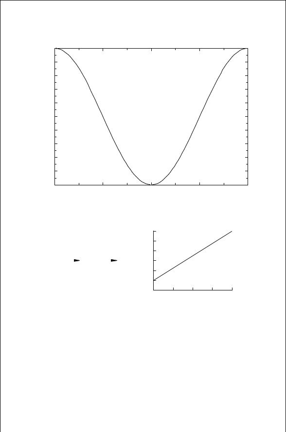
This is maximum when D 0°, a minimum when D 180°, and zero whenD 90° or 270° (Fig. 12.3).

When modeling a PLL in the frequency domain, the phase detector can be

modeled as


a


Kpd

12.5


a C s

which at low frequencies is simply the slope of the voltage with relation to the phase curve. The units for Kpd is volts/rad:

Kpd D

dVe

D

KmVaVb

sin

12.6

d

2

Thus Kpd D 0 when D 0° or 180° and a maximum absolute value at D 90° or 270°.

12.6.2Voltage-Controlled Oscillator

The voltage-controlled oscillator is the control element for a PLL in which the output frequency changes monotonically with the tuning voltage. A linear


PLL COMPONENTS

253


1.0


0.8


0.6


0.4


Voltage

0.2


0.0


Output

−0.2


−0.4


−0.6


−0.8


−1.0

90

180

270

360


0

Phase Difference

FIGURE 12.3 Phase detector voltage output as function of phase difference.

Tuning


Output

Voltage


Frequency

Vtune


fout


VCO


Frequency, MHz

600


500


400


300


200


100


0

0

2

4

8

10


Tuning Voltage


FIGURE 12.4 Voltage-controlled oscillator tuning.

frequency versus tuning voltage is an adequate model for understanding its operation (Fig. 12.4):

ωout D Kvco Ð Vtune C ω0

12.7

In a PLL the ideal VCO output phase may be expressed as


t


t D ω0t C KvcoVtunedt C 0

12.8

0

254 PHASE LOCK LOOPS

where ω0 is the free-running VCO frequency when the tuning voltage is zero and Kvco is the tuning rate with the dimension of rad/s-volt.

The error voltage from the phase detector first steers the frequency of the VCO to exactly match the reference frequency, and then holds it there with a constant phase difference. It is modeled as having a low-frequency gain Kvco and one or more poles of the following form:

Kvco

12.9

s s C a

12.6.3Loop Filters

A loop filter is a low-frequency circuit that filters the phase detector error voltage with which it controls the VCO frequency. While it can be active or passive, it is usually analog and very simple. In extreme cases it might be an entire microprocessor. This discussion will be limited to analog loop filters, such as the representative topologies shown in Fig. 12.5. Figure 12.5a shows an op-amp integrator with nearly infinite dc gain. This is the loop filter often associated with the type 2 PLL. The order and type of a PLL is defined in Section 12.9. Figure 12.5b shows an op-amp loop filter with a finite gain and is associated with a type 1 PLL. Figure 12.5c is a passive filter used with a phase detector whose output is current rather than voltage. This type of detector is frequently found in synthesizer ICs and is associated with a type 2 PLL. While the loop filter is a simple circuit, its characteristic is important in determining the final


Rp


Rs

C

Rs

C

Vpd

Rin

Vtune

Vpd Rin

Vtune


+


+


Type 2 PLL


Type 1 PLL


Vpd

R1

Vtune


R2

C

Type 2 PLL

FIGURE 12.5 Loop filter used in a (a) type-2 PLL, (b) type-1 PLL, and (c) type-2 PLL.

LINEAR ANALYSIS OF THE PLL [1]

255

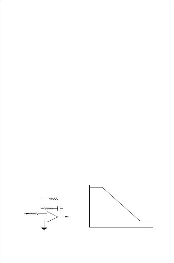
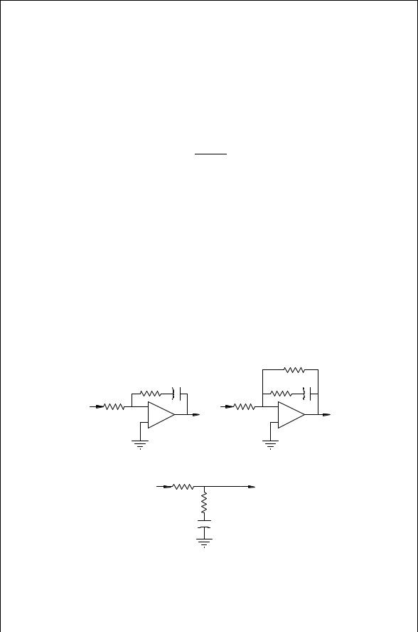
closed loop operation. The wrong design will make the loop unstable causing oscillation or so slow that it is unusable. The loop filters shown in Fig. 12.5 are modeled by

F s


s C a

12.10

D sn s C b s C c


where a is a zero and b and c are poles.

12.6.4Frequency Dividers

When the output frequency must be a multiple of the input frequency, frequency dividers may be included in a PLL. Most dividers are a digital circuit, although analog techniques dating from 1939 are available for very high frequency devision. With the availability of complete synthesizers on a single IC, fewer standalone divider circuits are on the market. Most dividers have a division ratio equal to a binary number or switchable from a binary to a binary C1 (e.g., divide by 64 or 65). The upper limit on the input frequency is about 3 GHz, although only a few ICs will go that high. Divide by four circuits has been demonstrated with inputs above 14 GHz, but this is a very specialized device not required by most PLLs. For a linear analysis when the loop bandwidth is much less than the reference frequency, dividers are modeled as a gain element with a value D 1/N.

12.7LINEAR ANALYSIS OF THE PLL [1]

From the perspective of the time domain, the control voltage for the VCO is


t


Vtune t D Vtune 0 t C

0

ve t f t d

12.11

where f t is the impulse response of the filter. Now the Laplace transform of f t is


1


F s

D

f t e stdt, t > 0

12.12


0


and the inverse transform can be obtained in principle by the contour integral shown below:

1

1


f t D


1 F s estds, <s > 0

12.13

2 i

† This material is based on A. J. Viterbi, Principles of Coherent Communication, 1966, by permission of the McGraw-Hill Company.

256 PHASE LOCK LOOPS

Then the VCO frequency is


d 2t


KmVaVb


t


D ω0 C


f t cos

12.14


dt


2


0

where t

D 1t


2t . Consequently, a the general equation describing

the phase error is


d d 1


KmVaVb


t


D


ω0


f t cos d

12.15


dt

dt


2

0

For a given input phase 1, the solution of this equation describes the exact operation of the PLL. However, to avoid carrying along ω0, a new phase variable may be defined:

1t


t

ω0t

12.16

D 1

2t


t

ω0t

12.17

D 2

The equation for the phase error is now given without ω0:

d d 1


KmVaVb


t


f t cos d

12.18


D


dt

dt

2

0

This suggests an alternate representation for the phase lock loop shown in Fig. 12.6. In this representation the multiplier is replaced by a subtracter and a cosinusoidal nonlinearity, while the VCO is replaced by an integrator.

When the phase error deviates from 90° by a small amount, cos C 90° ³ . Then Eq. (12.18) becomes


d

1


d


t


D

C K


f t d

12.19


dt


dt

0

where


KmVaVb


K D

12.20


2


f1(t)

∆f(t)

cosf


+

cos ( )

K

Filter f(t)


df2(t)


f2(t)


dt


dt


FIGURE 12.6 Time domain nonlinear phase lock loop.

LINEAR ANALYSIS OF THE PLL [1]

257

If the Laplace transform of 1 t is represented by Q s and the Laplace transform

of t

is represented by Q s , then the Laplace transform of Eq. (12.19) is


s Q s C KF s Q s D s Q 1 s

12.21

This linear frequency domain equation for the PLL can be represented as shown in Fig. 12.7.

The solution for the phase error gives

Q s D


Q 1 s

12.22

1

C

KF s /s


so that the phase shift at the output of the PLL is

Q 2 s D Q 1 s Q s


Q 2 s


G s

12.23


D P s D


Q 1 s

1

C

G s


where G s D VaVbKm/2F s /s. The phase error can in turn be written in terms of this transfer function:

Q s D Q 1 s Q 2 s D [1 P s ] Q 1 s

12.24

If, for example, the phase of the incoming signal is 1 t D ωt C 0 and the PLL has no filter, F s D 1. Readjusting the phase reference as was done in Eqs. (12.16) and (12.17) gives

1 D 1 ω0t


D ω ω0 t C 0

In the frequency domain this becomes


Q 1

s


ω ω0

0


D


s2

C

s


~

~


f1(s)

∆f(s)


+


K


F (s)


~


f2(s)


1/s


12.25

12.26

12.27

FIGURE 12.7 Frequency domain linear phase lock loop.

258 PHASE LOCK LOOPS

The phase error is found from Eq. (12.22):

s


1


ω ω0


0

12.28

D K/s s2

C s

Q


The inverse transform in this case is straightforward and gives the phase error in the time domain:

t

D

ω ω0

1


e Kt

C

e Kt

12.29


K


0


The steady state phase error is found by allowing t ! 1:


t

D 1 D


ω ω0


12.30


K


Clearly, the phase will change when the incoming frequency changes, so that phase lock is not achieved.

The insertion of a low-pass filter into the PLL will produce lock. An active filter such as that shown in Fig. 12.8 is recognized as basically a noninverting amplifier. The inverting amplifier has right half-plane poles and is therefore unstable. For the noninverting case the voltage gain can be found by writing node equations at the input nodes of the operational amplifier:

F s

D

Vo


1


R2 C 1/sC


1


R2


1

Vi

D

C

R1

D

C R1

C sCR1


The phase transfer factor is found from Eq. (12.23):

P s

D

Q 2 s

D

K[ 1 C R2/R1 R1Cs C 1]


Q 1 s

s2CR1 C CR1K 1 C R2/R1 s C K

Thus, using Eq. (12.24), the phase error is easily obtained:

Q [1 ]

s D P s 1 s


+


Vi

R2

C


R1


12.31

12.32

12.33

+

V0

FIGURE 12.8 Possible active low-pass filter for the PLL.

LOCKING A PHASE LOCK LOOP

259

s


ω ω0 CR1 C 0CR1s


12.34


Q

D s2CR

1 C

CR

K 1

C

R

/R

1

s

C

K


1


2


Rather than find the inverse transform this time, the final value theorem may be used to find the steady state phase error:

tlim t

lim s Q s

D

0

12.35

!1

D s 0


!


In this case the phase error is independent of frequency and in the steady state is zero.

12.8LOCKING A PHASE LOCK LOOP

The previous sections examined each of the elements in a PLL. As an example of how these parts go together, consider a simple loop with no frequency divider. Also assume that initially the loop is not locked and that the reference frequency is 100 MHz. A VCO tuning voltage of 5 volts is required to make the VCO frequency be 100 MHz. The phase detector can produce a cosine wave beat note of 1 volt peak to peak.

To simplify the design, a type 1 loop filter will be used. This is an inverting op-amp circuit with a gain of 100 at low frequency and a gain of 0.1 at high frequency (Fig. 12.9). With the loop unlocked, the VCO frequency could be anywhere within its operating limits. Assume that it is operating at 101 MHz, so that there is a 1 MHz beat note at the phase detector output when the reference frequency is first applied. This beat note frequency is high enough to only be amplified with a gain of 0.1 by the loop filter. The VCO tuning voltage will be modulated by the phase detector output of 0.1 volt peak to peak, but this voltage will not cause any significant change in the VCO frequency.

With the VCO frequency too far away from the reference frequency, there is not enough gain in the loop to bring the loop into lock. However, if the VCO


+60


Rp


C

dB


Rs

Gain,

Vpd

Rin


Vtune


+


−20


Beatnote Frequency, kHz

FIGURE 12.9 (a) Type 1 loop filter and (b) its frequency response.

Соседние файлы в предмете Электротехника