

Davis W.A.Radio frequency circuit design.2001
.pdf150 NOISE
R 2 |
|
(R 1+R 2) R 3 |
R 1 |
R 3 |
= < v 2 > + |
|
|
– |
FIGURE 8.3 Noise voltage from series and parallel resistors.
< i 2 > |
R |
C |
L < v 2 > |
FIGURE 8.4 Noise voltage from an RLC circuit.
f, which would be typically the case when the measured noise frequency, f, is approximately a sinusoid where f × f, then
v2 |
|
hi2i |
|
|
i D jG C j ωC 1/ωL j2 |
|
|||
h |
|
|||
|
D |
4kT fG |
8.25 |
|
|
|
|
||
|
jYj2 |
|||
If the output resistance varies appreciably over the range of the noise bandwidthf, then the individual noise “sinusoids” must be summed over the bandwidth, resulting in the following integral:
hv2i D 4kT |
G |
8.26 |
f jYj2 df |
As a simple example, consider the noise generated from a shunt RC circuit that would result from removing the inductance in Fig. 8.4:
hv2i D |
1 |
|
|
|
4kTGdf |
8.27 |
|||||||
0 G2 C ωC 2 |
|||||||||||||
D |
4kTG |
Ð |
|
G |
1 |
|
d ωC/G |
|
|||||
2 G2 |
|
C |
|
0 1 C ωC/G 2 |
|||||||||
|
2kT |
|
|
|
|
kT |
8.28 |
||||||
D |
|
Ð |
|
D |
|
|
|||||||
C |
2 |
C |
|||||||||||

AMPLIFIER NOISE CHARACTERIZATION |
151 |
This expression does not say that the capacitor is the source of the noise voltage. Indeed, experiments have shown that changing the temperature of the resistor is what changes the output noise. When the 3 dB frequency point of the circuit output impedance f3dB D 2 /RC is considered, the noise voltage in Eq. (8.28)
becomes
hv2i D 2 f3dBkTR
This looks similar to the Nyquist formula in its original form, Eq. (8.14).
8.5AMPLIFIER NOISE CHARACTERIZATION
One important quality factor of an amplifier is a measure of how much noise it adds to the signal while it amplifies it. The “actual noise figure,” F, is a convenient measure of how the amplifier affects the total output noise. The noise figure, which by the IEEE standards was considered analogous to “noise factor,” has been defined [7] as the ratio of (1) the total noise power per unit bandwidth at a corresponding output port when the standard noise temperature of the input termination is 290 K to (2) that portion of the total noise power engendered at the input frequency by the input termination. The standard 290 K noise temperature approximates the actual noise temperature of most input terminations as follows:
F D |
actual noise output power at T0 |
1 |
|
||
|
|
Ð |
|
|
|
available noise input power |
GT |
||||
D |
NTout |
8.29 |
|||
kT0GT f |
|
||||
In this expression GT is the transducer power gain, and T0 D 290 K. The noise figure is a measure of the total output noise after it leaves the amplifier divided by the input noise power entering the amplifier and amplified by an ideal noiseless gain GT. In an analog amplifier, the amplifier can only add noise, so F must always be greater than one. The noise figure can also be expressed in terms of the signal-to-noise ratio at the input to that at the output. If P represents the input signal power, then
P/kT0 f |
|
F D |
|
GTP/NTout |
|
Sin/NTin |
8.30 |
D Sout/NTout |
Since the signal-to-noise ratio will always be degraded as the signal goes through the amplifier, again F > 1. The expression (8.30) is strictly true only if the input temperature is 290 K. This is called the spot noise figure.
The portion of the total thermal noise output power contributed by the amplifier itself is
Na D NTout kT0GT f |
8.31 |
D F 1 kT0GT f |
8.32 |

152 NOISE
The factor, F 1, is used in two alternative measures of noise. One of these is noise temperature, which is particularly useful when dealing with very low noise amplifiers where the dB scale typically used in describing noise figure becomes too compressed to give insight. In this case the equivalent noise temperature is defined as
Te D T0 F 1 |
8.33 |
This is the temperature of the source resistance that when connected to the noisefree two-port circuit will give the same output noise as the original noisy circuit.
Another useful parameter for the description of noise is the noise measure [6]:
|
F 1 |
|
M D |
|
8.34 |
|
1 1/G |
|
This is particularly useful for optimizing a receiver in which, for example, a trade-off has to be made between a low-gain low-noise amplifier and a high-gain high-noise amplifier.
8.6NOISE MEASUREMENT
Measurement of noise figure can be accomplished by using a power meter and determining the circuit bandwidth and gain. However, it is inconvenient to determine gain and bandwidth each time a noise measurement is to be taken. The Y factor method for determining noise figure is an approach where these two quantities need not be determined explicitly. Actual noise measurements are done over a range of frequencies. The average noise figure over a given bandwidth is [7]
|
|
F f GT f df |
|
F |
D |
|
8.35 |
|
|||
|
|
GT f df |
|
This represents a more realistic expression for an actual measurement of noise figure than the spot noise figure.
An equivalent noise bandwidth f0 can be defined in terms of the maximum gain over the band as
GT f df D G0 f0 |
8.36 |
||||
so that |
|
||||
|
|
|
NTout |
8.37 |
|
|
F D |
||||
|
kT0G0 f0 |
|
|||
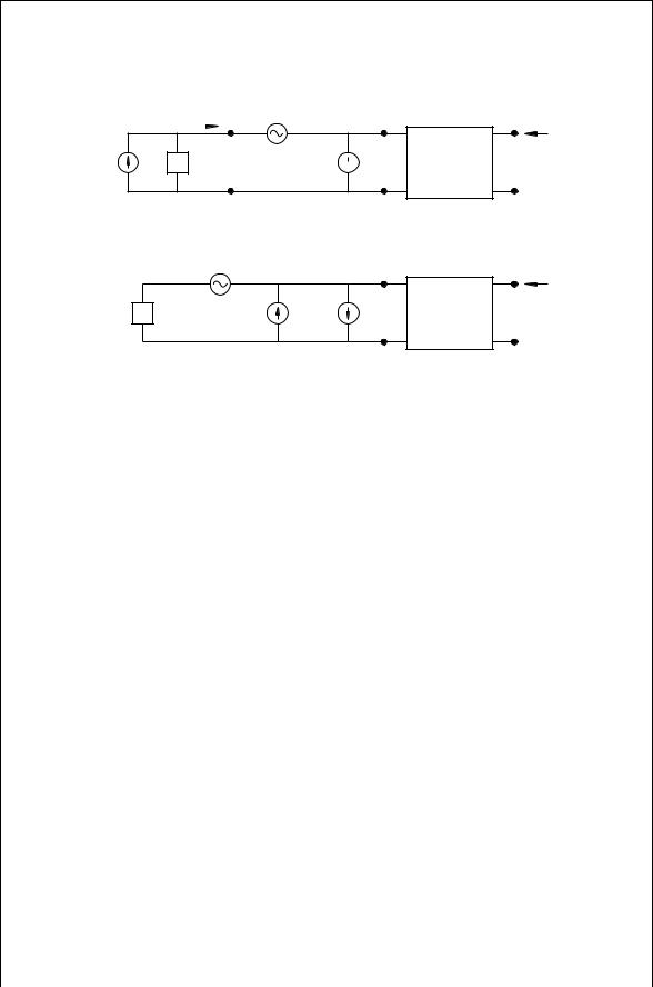
A measurement system that can be used to measure the noise figure of an amplifier is shown in Fig. 8.5. This excess noise source in this circuit is gated on and off to produce two values of noise measured at the output power detector, N1, and N2:
|
|
|
|
|
|
|
|
|
|
|
NOISY TWO-PORTS 153 |
|||
|
|
|
|
|
|
|
|
|
|
|
|
|
|
|
|
|
|
|
|
|
|
|
|
|
|
|
|
|
|
|
Input |
|
|
|
|
|
|
Amplifier |
|
Power |
|
|||
|
Termination |
|
|
|
|
|
|
G T |
Detector |
|
||||
|
|
|
|
Excess |
|
|||||||||
|
|
|
|
|
|
|
|
|
|
|
|
|
|
|
|
|
|
|
|
|
|
|
Noise |
|
|
|
|
|
|
|
|
|
|
|
|
|
|
|
|
|
|
|
|
|
|
|
|
|
|
|
|
|
Source |
|
|
|
|
|
|
|
|
|
|
|
|
|
|
|
|
|
||||
|
|
FIGURE 8.5 Noise measurement using the Y factor method. |
||||||||||||
|
Nex D calibrated excess noise source at T2 T0 |
|
|
|||||||||||
|
N1 D NTout when excess noise source is off |
|
|
|||||||||||
|
N2 D NTout when excess noise source is on |
|
|
|||||||||||
|
Nin D noise from input termination |
|
|
|||||||||||
|
Na D noise added by the amplifier itself |
|
|
|||||||||||
The Y factor as the ratio of N2 to N1 is easily obtained: |
|
|
||||||||||||
|
Y |
|
N2 |
|
G0Nin C G0Nex C Na |
|
8.38 |
|||||||
|
D N1 D |
G0Nin C Na |
||||||||||||
|
|
|
|
|||||||||||
DG0kT0 f0 C G0k T2 T0 f0 C F 1 kT0G0 f0 G0kT0 f0 C F 1 kT0G0 f0
DT2 T0 C FT0
|
|
FT0 |
|
|
|
|
When solved for |
|
, |
|
|
|
|
F |
|
T2 T0 |
|
|||
|
|
|
|
|
8.39 |
|
|
|
|
F |
D |
||
|
|
|
T0 Y 1 |
|||
|
|
|
|
|
||
Since a calibrated noise source is used, T2 T0 /T0 is known. Also Y is known from the measurement. The amplifier noise figure is then obtained. Modern noise measurement instruments implicitly use the Y factor.
8.7NOISY TWO-PORTS
The noise delivered to the output of a two-port circuit depends on the two-port circuit itself and the impedance of the input excitation source. The noise figure for a two-port circuit is given by the following:
Rn |
[ GG Gopt 2 C BG Bopt 2] |
8.40 |
F D Fmin C GG |

154 NOISE
Fmin D minimum noise figure
Rn D equivalent noise resistance (usually device data are given in terms of a normalized resistance, rn D Rn/50
YG D GG C jBG D the excitation source admittance
Yopt D Gopt C jBopt D optimum source admittance where the minimum noise figure occurs
While a designer can choose YG to minimize the noise figure, such a choice will usually reduce the gain somewhat. Sometimes the noise figure is expressed in terms of reflection coefficients, where
|
|
Y0 YG |
|
ZG Z0 |
8.41 |
|
G D Y0 C YG |
D ZG C Z0 |
|||||
|
|
|||||
where Y0 and Z0 are the characteristic admittance and impedance, respectively. Then the noise figure is given as follows:
F |
D |
F |
min C |
4r |
|
j G optj2 |
8.42 |
|
n 1 j Gj2 j1 C optj2 |
||||||||
|
|
|
|
|||||
The noise figure expression (8.40) and its equivalent (8.42) are the basic expressions used to optimize transistor amplifiers for noise figure. The derivation of Eq. (8.40) is the subject of the following section. Readers not wishing to pursue these details at this point may proceed to Section 8.9 without loss of continuity.
8.8TWO-PORT NOISE FIGURE DERIVATION
The work described here is based on the IRE standards published between 1956 and 1960 [8,9]. A noisy resistor can be modeled as a noiseless resistor in series with a voltage noise source. In similar fashion a two-port can be represented as a noiseless two-port and two noise sources. These two noise sources are represented in Fig. 8.6a as a voltage vn and a current in. The two-port circuit can be described in terms of its ABCD parameters and internal noise sources as
v1 D Av2 C Bi2 C vn
8.43
i1 D Cv2 C Di2 C in
or, as shown in Fig. 8.6, as a noiseless circuit and the noise sources referred to the input side. If the input termination, YG, produces a noise current, iG, then the circuit is completed. The polarity markings on the symbols for these sources merely point out the distinction between voltage and current sources. Being noise sources, the polarities are actually random. The Thevenin´ equivalent circuit in
TWO-PORT NOISE FIGURE DERIVATION |
155 |
i 1 |
1 |
|
|
|
|
i G |
Y G |
+
v n –
1' |
2 |
i 2
Noise i n  Free 2-Port
(a )
+
Y G
(b )
1 |
1' |
2 |
v n |
1' |
2 |
– |
||
|
|
i 2 |
i G |
i n |
Noise |
Free |
||
|
|
2-Port |
|
1' |
2 |
FIGURE 8.6 Equivalent circuit (a) for two-port noise calculation, and (b) the equivalent Theevenin´ circuit.
Fig. 8.6b shows that the short circuit current at the 10 –10 port is |
|
hisc2 i D hiG2 i C hjin C YGvnj2i |
8.44 |
D hiG2 i C hin2i C jYGj2hvn2i C YGŁ hvnŁini C YGhinŁvni |
8.45 |
The total output noise power is proportional to hi2sci, and the noise caused by the input termination source alone is hi2Gi. The part between 10 –10 and 2–2 is noise free; that is, it adds no additional noise to the output. All the noise sources are referred to the input side, so the noise figure is
F |
D |
hisc2 i |
8.46 |
|
hiG2 i |
||||
|
|
Part of the noise current source, in, is correlated and part is uncorrelated with the noise voltage vn. The uncorrelated current is iu. The rest of the current is correlated with vn and is given by in iu . This correlated noise current must be proportional to vn. The proportionality constant is the correlation admittance
given by Yc D Gc C jBc and is defined so that |
|
in D iu C Ycvn |
8.47 |
While this defines Yc, its explicit value in the end will not be needed. The mean value of the product of the correlated and uncorrelated current is of course 0. By definition, the average of the product of the noise voltage, vn, and the uncorrelated noise current, iu, must also be 0. Using the complex conjugate of

156 NOISE
the current (which is a fixed phase shift) will not change this fact: |
|
||||
|
hvniuŁi D 0 |
|
8.48 |
||
Rearranging Eq. (8.47) gives |
|
|
|
|
|
|
in iu |
D |
v |
n |
8.49 |
|
Yc |
||||
|
|
|
|||
The product of the noise voltage and the uncorrelated current in Eq. (8.48) can be expressed by substitution of Eq. (8.49) into Eq. (8.48):
h in iu iuŁi D 0 |
8.50 |
Because hvniŁui D 0 from Eq. (8.48), the product of the noise voltage and the correlated current can be found using Eq. (8.47):
hvninŁi D hvn in iu Łi D YcŁhvn2i |
8.51 |
The noise sources are determined by their corresponding resistances: |
|
hvn2i D 4kT0Rn f |
8.52 |
hiu2i D 4kT0Gu f |
8.53 |
hiG2 i D 4kT0GG f |
8.54 |
The resistance, Rn, is the equivalent noise resistance for hv2ni, and Gu is the equivalent noise conductance for the uncorrelated part of the noise current, hi2ui. The total noise current is the sum of the uncorrelated current and the remaining correlated current:
hin2i D hiu2i C hjin iuj2i |
|
D hiu2i C jYcj2hvn2i |
8.55 |
D 4kT0 f Gu C RnjYcj2 |
8.56 |
Now the expression for the short circuit current in Eq. (8.45) can be modified by Eq. (8.51):
hisc2 i D hiG2 i C hin2i C jYGj2hvn2i C YGŁ Ychvn2i C YGYcŁhvn2i |
8.57 |
Furthermore hi2ni can be replaced by Eq. (8.55):
hi2sci D hi2Gi C hi2ui C jYcj2hv2ni C jYGj2hv2ni C YŁGYchv2ni C YGYŁc hv2ni 8.58

TWO-PORT NOISE FIGURE DERIVATION |
157 |
The noise figure, given by Eq. (8.46), can now be put in more convenient form:
|
|
|
i2 |
|
v2 |
|
Yc |
j |
2 |
YG |
2 |
C |
YŁ |
Yc |
C |
YGYŁ |
|
|
F D 1 C |
h ui C h ni j |
|
|
C j j |
|
G |
|
|
c |
8.59 |
||||||||
|
|
|
|
|
i2 |
|
|
|
|
|
|
|
||||||
|
|
|
|
|
|
|
|
|
|
h Gi |
|
|
|
|
|
|
|
|
D |
1 |
|
4kT0Gu f C 4kT0Rn f jYGj C jYcj 2 |
|
8.60 |
|||||||||||||
|
|
|
||||||||||||||||
|
C |
|
|
|
4kT0GG f |
|
|
|
|
|
|
|||||||
D 1 C |
Gu |
C |
Rn |
[ GG |
C Gc 2 C BG C Bc 2] |
8.61 |
||||||||||||
GG |
GG |
|||||||||||||||||
The noise figure, F, is a function of the input termination admittance, YG, and reaches a minimum when the source admittance is optimum. In particular, the optimum susceptance is BG D Bopt D Bc. The value for Fmin is found by setting the derivative of F with respect to GG to zero and setting BG D Bc. This will determine the a value for GG D Gopt in terms of Gu, Ru, and Gc:
|
dF |
D 0 D |
Gu |
|
Rn |
|
GG C Gc 2 |
C |
2Rn |
GG C Gc |
8.62 |
|||||||
|
dGG |
G2 |
G2 |
|
GG |
|||||||||||||
|
|
|
G |
|
|
G |
|
|
|
|
|
|
|
|
|
|
||
Solution for GG yields |
|
|
|
|
|
|
|
|
|
|
|
|
|
|
|
|||
|
|
|
|
|
|
|
|
|
|
|
|
|
|
|
||||
|
|
G |
|
G |
D |
|
Gu C RnGc2 |
|
|
8.63 |
||||||||
|
|
|
|
|
|
|
|
|||||||||||
|
|
|
G D |
opt |
|
|
Rn |
|
|
|
|
|
|
|||||
or |
|
|
|
|
|
|
|
|
|
Gu |
|
|
|
|
|
|
||
|
|
|
|
Gc2 D Gopt2 |
|
|
|
|
|
|
8.64 |
|||||||
|
|
|
|
Rn |
|
|
|
|
|
|
||||||||
Substituting this into Eq. (8.61) provides the minimum noise figure, Fmin:
1 |
|
Gopt2 C 2Gopt |
Gopt2 |
|
Gu |
C Gopt2 |
|
Gu |
|
|||||
Fmin D 1 C |
|
Gu C Rn |
|
|
|
|
8.66 |
|||||||
Gopt |
Rn |
Rn |
||||||||||||
D 1 C 2Rn |
Gopt C |
Gopt2 |
|
Gu |
|
|
|
|
|
|
|
8.67 |
||
Rn |
|
|
|
|
|
|
|
|||||||
The correlation conductance, Gc, can be replaced from the total noise figure expression in Eq. (8.61) by Eq. (8.64) to give the following expression for F:
F D 1 C |
Gu |
C |
Rn |
|
|
|
|
|
|
|
|
|
|||
GG |
|
GG |
|
|
|
|
|
|
|
|
|
|
|
||
|
|
|
|
|
|
|
|
|
|
|
|
|
|
|
|
ð GG2 |
C 2GG Gopt2 |
|
Gu |
C Gopt2 |
|
Gu |
C BG Bopt 2 |
D 1 C |
Rn |
||||||
Rn |
|
Rn |
GG |
||||||||||||
158 NOISE
ð GG2 |
C 2GG Gopt2 |
Gu |
C Gopt2 2GGGopt C 2GGGopt |
C BG Bopt 2 |
||||||||||
Rn |
|
|||||||||||||
|
|
|
|
|
|
|
|
|
|
|
|
|
|
|
D 1 C |
Rn |
2GGGopt C 2GG |
|
Gopt2 |
Gu |
|
||||||||
GG |
|
|
Rn |
|
|
|||||||||
|
Rn |
|
|
|
|
|
|
|
|
|
|
|||
C |
|
[ GG Gopt 2 C BG Bopt 2] |
8.68 |
|||||||||||
GG |
||||||||||||||
Noting Eq. (8.67), the desired expression is obtained: |
|
|||||||||||||
|
|
|
|
|
F D Fmin C |
Rn |
[ GG Gopt 2 C BG Bopt 2] |
8.69 |
||||||
|
|
|
|
|
|
|||||||||
|
|
|
|
|
GG |
|||||||||
8.9THE FUKUI NOISE MODEL FOR TRANSISTORS
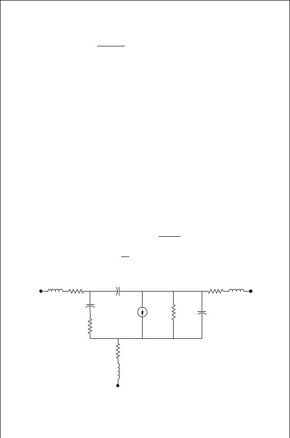
Fukui found an empirically based model that accurately describes the frequency dependence of the noise for high-frequency field effect transistors [10]. This model reduces to predicting the four noise parameters, Fmin, Rn, Ropt, and Xopt where the later two parameters are formed from the reciprocal of Yopt. For the circuit shown in Fig. 8.7, the Fukui relationships are as follows:
|
|
|
|
|
|
Rg C Rs |
1/2 |
|
F |
min D |
1 |
C |
k |
fC |
8.70 |
||
|
|
1 |
|
gs |
gm |
|
||
|
|
k2 |
|
|
|
|
8.71 |
|
|
Rn D gm |
|
|
|
|
|||
L g R g |
C gd |
|
|
|
|
|
R d L d |
|
C gs |
|
|
|
|
|
|
|
|
|
|
|
|
|
|
V i g m |
r o |
C ds |
R i
R s
L s
FIGURE 8.7 Equivalent circuit for noise calculation for a FET.

|
THE FUKUI NOISE MODEL FOR TRANSISTORS |
159 |
||||
Ropt D |
k3 |
1 |
C Rs C Rg |
8.72 |
||
|
|
|
|
|||
f |
4gm |
|||||
Xopt D |
k4 |
|
|
|
8.73 |
|
fCgs |
|
|
||||
In these expressions, f is the operating frequency in GHz, the capacitance is in pF, and the transconductance in Siemens. The constants k1, k2, k3, and k4 are empirically based fitting factors. The expression for Ropt in Eq. (8.72) differs from that originally given by Fukui, as modified by Golio [11]. The circuit elements of the equivalent FET model in Fig. 8.7 can be extracted at a particular bias level. The resistance, Ri, is often difficult to obtain, but for the purpose of the noise estimation, it may be incorporated with the Rg. The empirically derived fitting factors should be independent of frequency. They are not quite constant, but over a range of 2 to 18 GHz average values for these are shown below [11]:
k1 D 0.0259 k2 D 2.966 k3 D 14.51 k4 D 162.6
These values can be used for approximate estimates of noise figure for both metal semiconductor field effect transistors (MESFETs) as well as high-electron mobility transistors (HEMTs).
The transistor itself can be modified to provide either improved noise characteristics or improved power-handling capability by adjusting the gate width, W. The drain current, Ids, increases with the base width W. Consequently those equivalent circuit parameters determined by derivatives of Ids will also be proportional to W. Also the capacitance between the gate electrode and the source electrode or between the gate electrode and the drain electrode will be also proportional to W. This is readily seen from the layout of a FET shown in Fig. 8.8. The gate resistance, Rg, scales differently, since the gate current flows in the direction of the width. Also the number of gate fingers, N, will reduce the effective gate resistance. The gate resistance is then proportional to W/N. These relationships may be summarized as follows:
gm / W
1
Rds /
W
Cgs / W
Cgd / W
W
Rg /
N