

Davis W.A.Radio frequency circuit design.2001
.pdf170RF POWER AMPLIFIERS
iout
Q 1 on
Q 2 on
FIGURE 9.3 The reconstituted waveform of a class B amplifier.
transistors is cut off when the total voltage is less than 0, only the positive half of the wave is amplified. The conduction angle is 180°. The term, class AB amplifier, is sometimes used to describe the case when the dc bias current is much smaller than the signal amplitude, IOC, but still greater than 0. In this case,
180° < conduction angle − 360°
9.2.1Complementary (npn/pnp) Class B Amplifier
Figure 9.4a shows a complementary type of class B amplifier. In this case transistor Q1 is biased so that it is in the active mode when the input voltage, vin > 0.7 and cut off when the input signal vin < 0.7. The other half of the signal
|
V CC |
|
|
|
VCC |
|
|
|
|
V CC |
|
I Q |
|
|
I Q |
|
|
|
|
|
I Q |
|
|
Q 1 |
|
|
|
Q 1 |
|
|
|
Q 1 |
|
|
|
|
|
|
|
|
|
R 1 |
|
|
V b |
|
|
|
|
|
|
|
|
Q 4 |
|
|
|
|
|
|
|
|
R 2 |
|
|
|
|
|
R L |
|
|
|
|
R L |
R L |
|
|
|
Q 2 |
V b |
|
Q 2 |
|
|
|||
|
|
|
|
|
|
|
Q 2 |
|||
|
Q 3 |
|
|
+ |
Q 3 |
|
|
+ |
|
Q 3 |
v in |
+ |
|
v in |
–V |
|
|
|
|
||
–V |
CC |
|
CC |
v |
in |
|
–V CC |
|||
|
– |
|
– |
|
|
|
||||
|
|
|
|
|
|
– |
|
|
||
|
(a ) |
|
|
|
(b ) |
|
|
|
|
(c ) |
FIGURE 9.4 (a) The basic complementary class B amplifier, (b) class B amplifier with diode compensation to reduce crossover distortion, and (c) class B amplifier with a VBE multiplier to reduce crossover distortion.

THE CLASS B AMPLIFIER |
171 |
is amplified by transistor Q2 when vin < 0.7. When no input signal is present, no power is drawn from the bias supply through the collectors of Q1 or Q2, so the class B operation is attractive when low standby power consumption is an important consideration. There is a small region of the input signal for which neither Q1 nor Q2 is on. The resulting output will therefore suffer some distortion.
The npn transistor Q1 in the class B circuit in Fig. 9.4a has its collector connected to the positive power supply, VCC, and its emitter connected to the load, RL. The collector of the pnp output transistor, Q2, has its collector connected to the negative supply voltage VEE, which is often equal to VCC, and its emitter also connected to the load, RL. The bases of Q1 and Q2 are connected together and are driven by the collector of the input transistor Q3. The input transistor, Q3, has a bias current source, IQ feeding its collector, which also provides base current for Q1. The input voltage, vin to the input transistor Q3 is what drives the output stage. It is tempting when doing hand or SPICE calculations to start with vin. However, because a small change in base voltage of Q3 makes a large change in the collector voltage of Q3, it is easier to start the analysis at the base of Q2. This base voltage can be called VX.
When VX D 0, both the output transistors Q1 and Q2 are turned off because the voltage is less than the 0.7 volts necessary to turn the transistors on. If VX > 0.7, then Q1 (npn) is on and Q2 (pnp) is off. Current is then drawn from the power supply, VCC, through Q1 to produce the positive half-wave of the signal in the load. If VX < 0.7, then Q1 (npn) is off and Q2 (pnp) is on. The voltage VX is made negative by turning Q3 on thus bringing the collector voltage of Q3 closer to VEE which is less than zero. An extreme positive or negative input voltage puts the turned on output transistor (either Q1 or Q2) into saturation. The maximum positive output voltage is
VOC D VCC VCE1 sat |
9.3 |
and the maximum negative output voltage is
VO D VEE C VEC2 sat |
9.4 |
Typically the value for VCE sat ³ 0.2 volts for a bipolar transistor. More design details are available from a variety of sources, such as [1].
9.2.2Elimination of the Dead Band
The 1.2 to 1.4 volt range in the base voltages of Q1 and Q2 can be substantially compensated by addition of two diodes in series between the bases of Q1 and Q2 (Fig. 9.4b). These diodes are named, respectively, D4 and D5. For purposes of calculation, let VX stand for the voltage at the collector of the driver transistor Q3, which is the same as the base voltage for the pnp output transistor Q2. To get to the base of Q1 from VX now requires going through the two series-connected diodes “backwards,” from cathode to anode. If VX > 0 but not so high as to turn

172 RF POWER AMPLIFIERS
off the diodes D4 and D5, then Q1 is on as described Fig. 9.4a. The voltage across the load is
VOC D VX C VD4 C VD3 VBE1 |
9.5 |
To make VX < 0, the input voltage to the driver Q3 must be a positive voltage. The npn output transistor Q1 is turned off, and the excess bias current from IQ flows through the diodes D4 and D5 and then through the now turned on Q3. The output voltage is not affected directly by the diodes now:
VO D VEB2 C VX |
9.6 |
Under this condition, the value of VX is actually a negative number. In the middle when VX D 0, the output voltage across RL is
VOC D VD4 C VD5 VBE1 ³ VBE |
9.7 |
and |
|
VO D VBE2 D VBE |
9.8 |
If the forward diode voltage drops are equal to the base–emitter drops of the transistors, there is no discontinuity in VO in going from negative to positive input voltages.
In actual production circuits, tight specifications are needed on diodes D4 and D5, since they are in the base circuit of the output transistors and consequently carry much less current than the output power devices. The discrepancy between the high-power and low-power devices can be alleviated by using the VBE multiplier shown in Fig. 9.4c. In this circuit the base–emitter voltage of Q4 sets the current through R2:
IR2 D |
VBE4 |
9.9 |
R2 |
Assuming the base current of Q4 is negligible, the voltage drop between the bases of the output transistors Q1 and Q2 is
|
R2 |
|
|
|
|||
VCE4 D IR2 R1 C R2 D VBE4 |
|
|
C 1 |
|
D VBE1 C VEB2 |
9.10 |
|
R1 |
|
||||||
When the voltage at the base of Q2 is positive, the load voltage is |
|
||||||
VOC D VX C VBE4 |
|
R2 |
1 |
VBE1 |
9.11 |
||
|
|
C |
|||||
|
R1 |
||||||
and where VX < 0, |
|
|
|
|
|
|
|
VO D VEB2 C VX |
|
9.12 |
|||||

THE CLASS B AMPLIFIER |
173 |
In the middle where VX D 0 the VCO and VO can be forced to be equal by adjustment of the resistors R1 and R2,
R2 |
C 1 VBE1 D VEB2 |
9.13 |
VO D VBE4 R1 |
In addition to reducing or eliminating the dead band zone, the compensation circuits in Fig. 9.4b and 9.4c also provide for temperature stability, since a change in the temperature changes the transistor VBE value. The compensation circuit and the power transistors vary in the same way with temperature, since they are physically close together.
Another aspect that deserves attention is the actual value of the current source, IQ. Since this supplies the base current for the npn output transistor Q1, IQ must be large enough to not “starve” Q1 when it is drawing the maximum current through its collector. This means that IQ ½ IC1/ˇ1.
9.2.3The Composite pnp Transistor
One of the primary problems in using this type of class B amplifier is the requirement for obtaining two equivalent complementary transistors. The problem fundamentally arises because of the greater mobility of electrons by over a 3 : 1 factor over that of holes in silicon. The symmetry of the gain in this circuit depends on the two output transistors having the same short circuit base to collector current gain, ˇ D ic/ib. When it is not possible to obtain a high ˇ pnp transistor, it is sometimes possible to use a composite transistor connection. A high-power npn transistor, Q1, is connected to a low-power low ˇ pnp transistor, Q2, as shown in Fig. 9.5. Normally the base–emitter junctions of the composite and single pnp transistor are forward biased so that the Shockley diode equation may be used to describe the bias currents. For Q2 in the composite circuit,
|
|
IC2 D ISeqVEB/kT |
9.14 |
|
|
E |
E |
|
|
I E |
I E |
|
I B |
|
I B |
B |
Q 1 |
= |
B |
|
|
Q 2 |
|
|
I C1 |
|
|
|
|
I C |
I C |
|
|
C |
C |
FIGURE 9.5 A composite connection for a pnp transistor.

174 RF POWER AMPLIFIERS
The collector current for Q1 in the composite circuit is the same as the collector current for the single pnp transistor:
IC D ˇ1 C 1 IC2 D ˇ1 C 1 ISeVBE/kT |
9.15 |
The composite circuit has the polarity of a pnp transistor with the gain of an npn transistor.
9.2.4Small Signal Analysis
The three fundamental parameters that characterize an amplifier are its voltage gain, Av, input resistance, Rin, and output resistance, Rout. In the circuit shown in Fig. 9.4a, neither Q1 nor Q2 are on simultaneously. If Q1 is on, Q2 is an open circuit and need not be considered as part of the ac analysis. A small signal hybrid model (Fig. 9.6) for a bipolar transistor consists of a base resistance, rb, base–emitter resistance, r , collector–emitter resistance, ro, transconductance, gm, and short circuit current gain ˇ D gmr . There are in addition high-frequency effects caused by reactive parasitic elements within the device. Since the voltage gain of an emitter follower is ³ 1, the voltage gain of the Q3 and Q1 combination is
Av D gm3RL eff |
9.16 |
The effective load resistance RL eff seen by the first transistor, Q3, is the same as the input resistance of the emitter follower circuit Q1. Circuit analysis of the low-frequency transistor hybrid model would give (Appendix F)
RL eff D r 1 C rb1 C ˇ1 C 1 ro1jjRL |
9.17 |
|||
|
³ ˇ1RL |
|
|
9.18 |
|
r |
|
|
|
r b |
C |
|
|
r c |
|
|
|
||
C p |
r p |
g mV p |
r ο |
C cs |
|
r ex |
|
|
|
FIGURE 9.6 The small signal hybrid model of a bipolar transistor.
THE CLASS B AMPLIFIER |
175 |
The voltage gain is then found by substitution: |
|
AvC D gm3[r 1 C rb1 C ˇ1 C 1 ro1jjRL ] |
9.19 |
³ gm3ˇ1RL |
9.20 |
The low-frequency input resistance to the actual class B amplifier is given by RL eff in Eq. (9.17), and the output resistance is
R |
out D |
r C Rbb C rb |
9.21 |
||
|
|||||
|
1 |
C |
ˇ |
|
|
|
|
|
|
|
|
Thus the input resistance is high and the output resistance is low for a class B amplifier, which enables it to drive a low-impedance load with high efficiency.
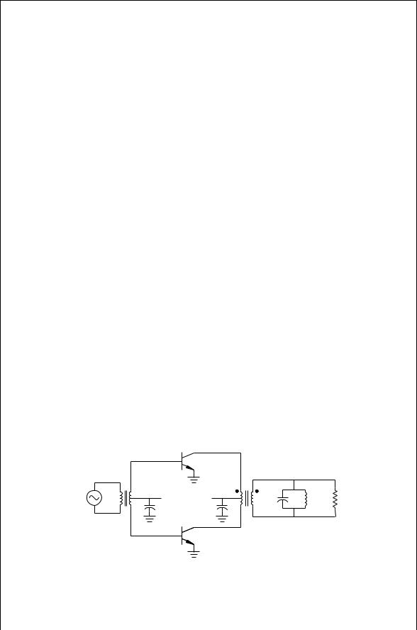
9.2.5All npn Class B Amplifier
The complementary class B amplifier shown in Fig. 9.4 needs to have symmetrical npn and pnp devices. In addition this circuit also requires complementary power supplies. These two problems can be alleviated by using the totem pole or all npn transistor class B amplifier. This circuit requires only one power supply, and it has identical npn transistors that amplify both the positive and negative halves of the signal. However, it requires that the two transistors operate with an input phase differential of 180°. This circuit is illustrated in Fig. 9.7. Clearly, the cost of the all npn transistor amplifier is the added requirement of two centertapped transformers. These are necessary to obtain 180° phase difference between Q1 and Q2. The center tapped transformer also provides dc isolation for the load. When the input voltage is positive, Q1 is on and Q2 is off. When the input voltage is negative, the input transformer induces a positive voltage at the “undotted” secondary winding which turns Q2 on. The output of Q2 will induce on the output transformer a positive voltage on the “undotted” terminal and a negative voltage on the “dotted” terminal. The negative input voltage swing is thus replicated as a negative voltage swing at the output. The transformer turns
Q 1
R L
+
v |
in – |
V |
BB |
V |
CC |
C |
L |
R ' |
L |
|
|
|
|
|
|
||||
|
|
|
|
Q 2 |
1 : n |
|
Filter |
|
|
|
|
|
|
|
|
|
|
|
FIGURE 9.7 The all npn class B amplifier.

176 RF POWER AMPLIFIERS
ratio can be used for impedance matching. The output filter is used to filter out any harmonics caused by crossover or other sources of distortion. The filter is not necessary to achieve class B operation, but it can be helpful.
9.2.6Class B Amplifier Efficiency
The maximum efficiency of a class B amplifier is found by finding the ratio of the output power delivered to the load to the required dc power from the bias voltage supply. In determining efficiency in this way, power losses caused by nonzero base currents and crossover distortion compensation circuits used in Fig. 9.4b and 9.4c are neglected. Furthermore the power efficiency rather than the power added efficiency is calculated so as to form a basis for comparison for alternative circuits. It is sufficient to do the calculation during the part of the cycle when Q1 is on and Q2 is off. The load resistance in Fig. 9.7 is transformed through to the primary side of the output transformer, loading the transistors with a value of RL.
The magnitude of the collector current that flows into RL is IOC. The ac current is
io ωt D IOC sin ωt |
9.22 |
and the voltage is |
|
vo ωt D IOCRL sin ωt |
9.23 |
Since the collector–base voltage must remain positive to avoid the danger of burning out the transistor, VO C D IOCRL VCC. The maximum allowable output power delivered to the load is
VO 2
Po D C 9.24 2RL
Now a determination of the dc current supplied by the bias supply is needed. The magnitude of the current delivered by the bias supply to the load by Q1 is
iBB1 D IOC sin ωt , |
0 < ωt < |
9.25 |
and for Q2, |
|
|
iBB2 D IOC sin ωt , |
< ωt < 2 |
9.26 |
The total current is then IOCj sin ωt j, which is shown in Fig. 9.8. The dc current from the bias source(s) is found by finding the average current:
1 |
|
T/2 |
IOC1 sin ωtdt |
|||
Idc D |
|
0 |
|
|||
T |
||||||
|
|
|
IOC1 |
|
T/2 |
|
|
|
|
|
|
||
D |
|
cos ωt |
|
|||
ωT |
0 |
|||||

THE CLASS B AMPLIFIER |
177 |
I C
Idc
FIGURE 9.8 Waveform for finding the average dc current from the power supply.
|
|
|
IOC1 |
|
|
2 T |
|
T/2 |
||||||
D |
|
cos |
1 |
|
||||||||||
|
|
|
|
|
|
|
|
|
|
|||||
2 /T T |
T 2 |
0 |
||||||||||||
|
|
IOC1 |
|
|
|
|
|
|
||||||
D |
|
[ 1 |
1] |
|
|
|
|
9.27 |
||||||
2 |
|
|
|
|
||||||||||
Idc D |
IOC1 |
D |
1 VO |
|
|
|
|
|
9.28 |
|||||
|
|
|
RL |
|
|
|
|
|
||||||
The power drawn from both of the power supplies by both of the output transistors is
2 VCC |
Ð VO |
|
Psupply D 2VCCIdc D RL |
9.29 |
Thus the output power is proportional to VO, and is the average power drawn from the power supply. The power delivered to the load is
P |
jVOj2 |
9.30 |
|
2RL |
|||
L D |
|
The efficiency is the ratio of these latter two values:
|
|
|
PL |
|
jVOj2 |
|
|
|
RL |
9.31 |
|
D Psupply |
D |
2RL 2 |
|
VCCVO |
|||||||
|
|
|
|||||||||
D |
VO |
|
|
|
|
|
|
9.32 |
|||
|
|
|
|
|
|
|
|
|
|||
4 VCC |
|
|
|
|
|
|
|||||
The maximum output power occurs when the output voltage is VCC VCE sat :
P |
|
1 |
|
|
VCC VCE sat 2 |
|
|
9.33 |
|||
|
2 |
|
|
|
|||||||
L max D |
|
|
|
RL |
|
|
|
|
|||
|
max D |
|
|
VCC VCE sat |
³ |
78.5% |
9.34 |
||||
4 |
VCC |
||||||||||
|
|
|
|
|
|||||||
This efficiency for the class B amplifier should be compared with the maximum efficiency of a class A amplifier, where max D 25% when the bias to the collector

178 RF POWER AMPLIFIERS
is supplied through a resistor and max D 50% when the bias to the collector is supplied through an RF choke.
9.3THE CLASS C AMPLIFIER
The class C amplifier is useful for providing a high-power continuous wave (CW) or frequency modulation (FM) output. When it is used in amplitude modulation schemes, the output variation is done by varying the bias supply. There are several characteristics that distinguish the class C amplifier from the class A or B amplifiers. First of all it is biased so that the transistor conduction angle is <180°. Consequently the class C amplifier is clearly nonlinear in that it does not directly replicate the input signal like the class A and B amplifiers do (at least in principle). The class A amplifier requires one transistor, the class B amplifier requires two transistors, and the class C amplifier uses one transistor. Topologically it looks similar to the class A except for the dc bias levels. It was noted that in the class B amplifier, an output filter is used optionally to help clean up the output signal. In the class C amplifier, such a tuned output is necessary in order to recover the sine wave. Finally, class C operation is capable of higher efficiency than either of the previous two classes, so for the appropriate signal types they become very attractive as power amplifiers.
The class C amplifier shown in Fig. 9.9 gives the output circuit for a power bipolar transistor (BJT) with the required tuned circuit. An N-channel enhance- ment-mode metal oxide semiconductor field effect transistor (MOSFET) can be used in place of the BJT. The Q of the tuned circuit will determine the bandwidth of the amplifier. The large inductance RF coil in the collector voltage supply ensures that only dc current flows there. During that part of the input cycle when the transistor is on, the bias supply current flows through the transistor and the output voltage is approximately 90% of VCC. When the transistor is off, the supply current flows into the blocking capacitor. The current waveform at the
|
|
|
+ |
Vcc |
|
|
|
– |
|
|
|
|
RFC |
|
|
R G |
C B |
C B |
|
|
|
|
||
|
+ |
RFC |
C o |
R L |
VGsinωt |
|
|
L o |
|
– |
|
+ |
|
|
|
Vbb |
|
|
|
|
|
– |
|
|
|
|
|
|
FIGURE 9.9 A simple class C amplifier where VBB determines the conduction angle.

THE CLASS C AMPLIFIER |
179 |
ic
|
|
idc |
IC |
ψ 
FIGURE 9.10 The collector current waveform for class C operation.
collector can be modeled as the waveform shown in Fig. 9.10:
iC ωt |
D |
IC IOC sin ωt , |
|
ωt C |
9.35 |
|
0, |
otherwise |
|
||
For class C operation, the magnitude of the quiescent current is jICj < IOC. The point where quiescent current equals the total current is
3 |
š D 0 D IC IOC sin |
3 |
|
|
iC |
|
|
š |
|
2 |
2 |
|||
|
|
0 D IC C IOC cos |
|
9.36 |
This determines the value of the quiescent current in terms of the conduction angle 2 :
IC D IOC cos |
9.37 |
The dc current from the power supply is the average of the total collector current iC " :
|
1 |
|
2 |
|
|
Idc D |
|
iC " d " |
|
||
|
|
|
|
||
2 |
0 |
|
|||
|
1 |
|
3/2 C |
|
|
D |
|
|
|
IC IOC sin " d " |
|
2 |
|
|
|||
|
|
|
3/2 |
|
|
D |
1 |
|
IC C IOC sin |
9.38 |
|
|
|||||
|
|||||