

Broadband Packet Switching Technologies
.pdfOPTOELECTRONIC PACKET SWITCHES |
289 |
11.2.4BNR Switch
Munter et al. introduced a high-capacity packet switch based on advanced electronic and optical technologies w20x. The main components of the switch are input buffer modules, output buffer modules, a high-speed switching core, and a central control unit, as shown in Figure 11.7. The core switch contains a 16 16 cross-connect network using optical links running at 10 Gbitrs.
The central control unit receives requests from input buffer modules and returns grant messages. Each request message indicates the number of queued packets in the input buffer module, which is later used to determine the size of burst allowed to transmit to the switch fabric. A connection can only be made when both input and output ports are free. A control bus is used by the free input ports to broadcast their requests, and by the free output ports to return grant messages.
An arbitration frame consists of 16 packet time slots for a 16 16 core switch. In each slot, the corresponding output port polls all 16 inputs. For example, in time slot 1, output port 1 Žif it is idle. will choose the input that has the longest queue destined for output port 1. If the input is busy, another input port that has the second longest queue will be examined. This operation repeats until a free input port is found. If a match is found Žfree input, free output, and outstanding request., a connection is made for the duration corresponding to the number of packets queued for this connection. So the switch is a burst switch, not a packet switch. In time slot 2, output port 2
Fig. 11.7 Diagram of BNR switch.
290 OPTICAL PACKET SWITCHES
repeats the above operation. The switch capacity is limited by the speed of the central control unit. Packet streams can have a long waiting time in the input buffer modules under a high traffic load.
11.2.5Wave-Mux Switch
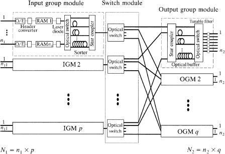
Nakahira et al. introduced a photonic ATM switch based on input output buffering w21x. Basically, this switch consists of three kinds of modules: the input group module ŽIGM., switching module ŽSWM., and output group module ŽOGM., as shown in Figure 11.8. They are connected by means of fiber optical lines. The inputs are divided into p groups of size n1, and each group is connected to an IGM. The cells arriving through optical lines are first converted to electronic signals by optical-to-electronic converters, and their header information is electrically processed at the header converter in IGMs. Both the header and the payload of the arriving cell are processed and stored in an electronic random access memory ŽRAM.. An optical sorter in each IGM is used to sort the cells with respect to their OGM requests and delivers them to the SWM in one cell slot time.
There are p optical switches in the SWM. Each optical switch transmits optical wavelength multiplexed cells from IGM to OGM. In each cell time slot, these p optical switches deliver at most p trunks of wavelength-multi- plexed cells from IGMs, which are destined to the different OGMs. In each
Fig. 11.8 Architecture of the wave-mux switch. Ž 1995 IEEE..
THE 3M SWITCH |
291 |
OGM, it is possible to have the cells with different wavelengths but with the same output port request. This is called output port contention and is solved by the use of an optical buffer. This optical buffer in the OGM is based on the fiber delay line principle. If no competing cells to the same output port are present in the optical buffer, the incoming wavelengths will be sent through the shortest optical fiber line. They are distributed to the tunable filters by an optical switch. Each tunable filter is then tuned to the wavelength of the requested output port.
The proposed optical switch architecture needs complex arbitration to solve the contention problem, not only for the cells in the same IGM but for the cells in the different IGMs as well. This will increase the complexity of control and thus limit the switch size. In this switch, in order to avoid HOL blocking, cells destined to the same OGM can be read out of the RAM with a speedup factor of two. Many optical-to-electronic and electronic-to-optical converters are required in the switching path, increasing the implementation cost.
11.3THE 3M SWITCH
The WDM ATM multicast Ž3M. switch is an optically transparent ATM switch w22, 23x By taking advantage of both optical and electronic technologies, it is proposed to route ATM cells through an optical switching plane, while extracting and processing their headers in an electronic plane that controls the optical devices and routes the cells to the proper output portŽs..
11.3.1Basic Architecture
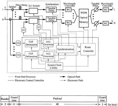
Figure 11.9 shows the architecture of an enhanced N N 3M switch, where incoming cells running at 2.5 Gbitrs are optically split into two paths. Cells on the top path remain in the optical domain and are routed through the optical switch plane. Cells on the bottom path are converted to the electronic domain, where their headers are extracted for processing Že.g., finding the output ports for which the cells are destined and finding new VPIrVCI values to replace the old ones.. An electronic central controller, as shown in Figure 11.9, performs cell delineation, VCI overwrite, cell synchronization, and routing. The first three functions are implemented in the photonic ATM front-end processor, while the last one is handled by a route controller that routes cells to proper output ports.
As shown in Figure 11.10, the cell format adopted in the system has 64 bytes with 5 bytes of header, 48 bytes of payload, and two guard time fields Žwith all ones., which are 6 and 5 bytes long, respectively. The guard times are used to accommodate the slow switching of optical devices such as optical tunable filters. The lengths of the guard times between the cells, and between the cell header and the payload, were chosen arbitrarily. Cells are transmitted back-to-back and not carried in SONET frames. Not using SONET
292 OPTICAL PACKET SWITCHES
Fig. 11.9 Architecture of the WDM ATM multicast Ž3M. switch. Ž 2000 IEEE..
Fig. 11.10 Cell format adopted in the system.
frames eliminates the possibility of having variable gaps between or within cells caused by the need to carry SONET transport and path overhead ranging from 1 to 49 bytes.
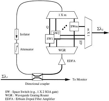
The incoming optical cells are first delayed by fiber lines, processed for their headers, and synchronized in the front-end processor before they are sent to the switch fabric. In the switch fabric, cells are converted to different wavelengths by wavelength converters ŽWCs. that are controlled by the route controller, which keeps track of the available wavelengths in the WDM optical shared memory. It is a fiber-loop memory, as shown in Figure 11.11, and is used to store optical cells until they are ready to be transmitted to the next node. Using a 3-dB directional coupler, cells are coupled into the optical memory and coexist with the existing cells. Accessing cells in the optical memory is done by controlling the 1 2 space switches ŽSWi. for example, SOA gates. The wavelengh-division multiplexed cell stream is amplified by an erbium-doped fiber amplifier ŽEDFA. to compensate power loss when looping in the memory. The cell stream is then demultiplexed by a waveguide
THE 3M SWITCH |
293 |
Fig. 11.11 An optical random access memory. Ž 2000 IEEE..
grating router ŽWGR. into m different channels, each carrying one cell. The maximum number of cells Ži.e., wavelengths. simultaneously stored in this memory has been demonstrated to be 23 circulations at 2.5 Gbitrs. Cells read from the WDM optical shared memory are broadcast to all N output ports by a 1 N splitter and selected by the destined output port Žor ports, if multicast. through tunable filters that are tuned by the route controller on a per-cell basis. The final WC stage converts cells to their predetermined wavelengths. Other optical loop memory can be found in w25, 26, 27, 28, 29x.
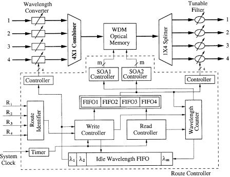
Figure 11.12 shows how the shared memory is controlled by a route controller. Signals R1 to R4 carry the output port addresses for which the cells are destined. An idle-wavelength FIFO keeps track of available wavelengths in the memory. When up to four incoming cells arrive, free wavelengths are provided by the idle-wavelength FIFO, and are used to convert incoming cells’ wavelengths so they can be written to the loop memory at the same time. These wavelengths are stored in the FIFOs ŽFIFO 1 to FIFO 4. according to the R1 to R4 values. Since the 3M switch supports multicasting, the same wavelength can be written into multiple FIFOs. All the FIFOs Žincluding the idle wavelength one. have the same depth, storing up to m wavelengths. While the wavelength values are written sequentially Žup to four writes in each cell slot. to the FIFOs, the wavelengths of the HOL cells of the FIFOs are read simultaneously, so that up to four cells can be read out
294 OPTICAL PACKET SWITCHES
Fig. 11.12 An optical shared memory controlled by a route controller. Ž 2000 IEEE..
simultaneously. They are, in turn, used to control the tunable filters to direct the cells to the proper output ports. The write controller and read controller generate proper signals to coordinate all functional blocks.
The header of an ATM cell carries all necessary information for routing. The photonic ATM front-end processor is designed to extract the cell header and perform the functions, including cell delineation, VCI overwrite, and cell synchronization. The three basic units to perform these functions are described in the following.
11.3.2Cell Delineation Unit
As shown in Figure 11.9, an optical cell stream is tapped from each input line, converted to electronic format, and sent to the cell delineation unit. Cell delineation is a process used to identify cell boundaries so that the incoming cell stream can be further processed at the cell level by the following units, such as VCI overwrite.
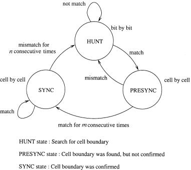
The standard HEC checking mechanism to find cell boundaries is adopted. It takes advantage of the inherent cyclic redundancy check ŽCRC. coding correlation between the cell header to be protected Žthe first 4 bytes. and HEC byte Žthe fifth byte of the cell header.. Figure 11.13 shows the state
THE 3M SWITCH |
295 |
Fig. 11.13 State diagram of cell delineation.
diagram of cell delineation. Initially, a cell boundary is arbitrarily assumed and checked by performing a polynomial division bit by bit in the HUNT state ŽFigure 11.13.. If the remainder Žthe syndrome. for a complete calculation is zero, then this boundary is assumed to be correct. Otherwise, shift a bit from the data stream and repeat the operation until the syndrome is zero. Once a cell boundary is determined, it is then confirmed cell by cell for eight consecutive times in the PRESYNC state before the cell boundary is claimed to be found. It then goes to the SYNC state. Once in the SYNC state, the cell boundary is claimed to be lost when seven consecutive mismatches occur. As a result, the above procedure for cell delineation will start over again Žfrom the HUNT state..
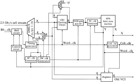
As shown in Figure 11.14, to reduce the high-speed circuit requirement, the serial bit stream at 2.5 Gbitrs is first converted to 16-bit parallel words Ž155 Mbitrs. through a serial-to-parallel converter. A 16-bit parallel format of the CRC circuit is used to perform polynomial division, and the syndrome is checked every three word clock cycles. An HPS ŽHUNT, PRESYNC, and SYNC. finite state machine performs the state transition between HUNT, PRESYNC, and SYNC states in Figure 11.13. If a syndrome equals zero, then the finite state machine goes to the PRESYNC state from the HUNT state and disables a set of control and shift circuits by a signal Y. Otherwise,
296 OPTICAL PACKET SWITCHES
Fig. 11.14 Block diagram of the cell delineation unit. Ž 2000 IEEE..
the finite state machine notifies the control and shift circuits to inhibit a bit or a byte every three cell clock cycles. Once the cell boundary is confirmed, the state machine goes to the SYNC state and sends a signal X to create a cell clock, which indicates the location of the cell boundary. The cell clock and signal X are passed to the VCI-overwrite unit together with the old VPIrVCI and the word clock.
Identifying cell boundaries for a back-to-back cell stream at 2.5 Gbitrs without using SONET frames is much more difficult than in the case where cells are carried over SONET frames. When an error HEC is detected in the HUNT state, a clock pulse at 2.5 GHz Žor 200 ps. is masked and the HEC hunting process is restarted, rather than shifting one byte as in the case where cells are carried over SONET frames.
11.3.3VCI-Overwrite Unit
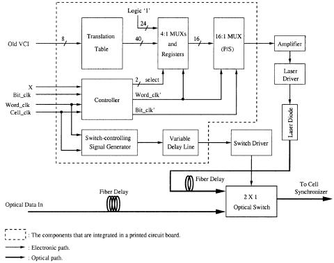
Once cell boundaries are recognized and confirmed by the cell delineation unit, the state machine moves to the SYNC state and enables the VCI-over- write unit with the cell clock and signal X, as shown in Figure 11.15. The main function of this unit is to overwrite the VPIrVCI field of the incoming cell header in the optical domain. The VCI-overwrite unit performs table lookups in the electronic domain, converts the new VPIrVCI to an optical signal, and replaces the old VPIrVCI by using a 2 1 optical switch. The routing table Ži.e., VPIrVCI translation table. is preprogrammed manually.
THE 3M SWITCH |
297 |
Fig. 11.15 Block diagram of the VCI-overwrite unit.
The challenge is to handle the high-speed overwriting at the bit rate of 2.5 Gbitrs with each bit only 400 ps long. It is solved by using electronic variable delay lines Žprogrammable delay. to compensate for the time difference between the old header and the new header.
As shown in Figure 11.15, the new header obtained from the table lookup is converted to a serial format by a parallel-to-serial converter. It is then used to control a laser driver to drive a DFB laser diode that generates the cell header in the optical domain. The new header replaces the old one using a 2 1 optical switch that is controlled by a 6-byte-wide pulse in every cell time slot. The successfully overwritten cells are sent to fiber delay lines in the cell synchronization unit.
11.3.4Cell Synchronization Unit
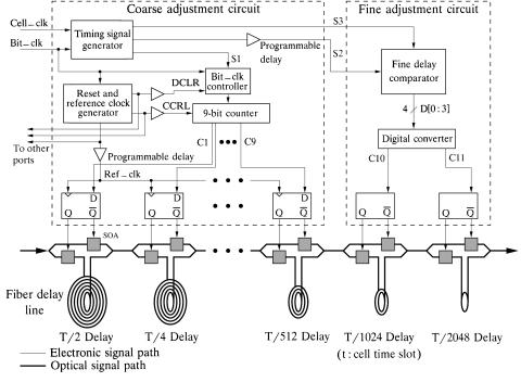
The cell synchronization unit is used to align the phases of incoming ATM cells in the optical domain. The synchronization issue is also addressed in w30x. Burzio et al. w31x and Zucchelli et al. w32x have implemented a two-stage cell synchronizer Žcoarse and fine synchronizer. at the rate of 622 Mbitrs. The former uses a few slow thermo-optic 2 2 switches to control the cells
298 OPTICAL PACKET SWITCHES
Fig. 11.16 Block diagram of the cell synchronization unit.
through different fiber delay lines. The latter uses a tunable wavelength converter to convert the wavelength of the cells so as to finely adjust the delay along a highly dispersive fiber.
In the 3M switch, synchronization is done at two levels. The cell contention resolution, VPIrVCI overwrite, and cell read Žwrite. from Žto. the loop memory are executed at the cell level, while the interaction between electronic and optical signals is at the bit level. For instance, cell header overwrite is done optically at the bit level. Furthermore, synchronization among the incoming optical cells is achieved at 14 bit.
The cell synchronization unit in Figure 11.16 is used to optically align cells from different inputs to the extent of 14 bit Ž100-ps, or 2-cm, optical delay line at 2.5 Gbitrs. before they are further processed in the switch fabric. Because of the stringent timing requirement, control is divided into two steps. A coarse adjustment circuit controls the first nine stages of the optical delay elements and adjusts the phases of incoming cells down to the bit level. A fine adjustment circuit controls the last two stages and further adjusts the phase down to 14 bit.
Each stage of the optical delay element consists of a Y-junction SOA gate, a combiner, and a fiber delay line with a delay of Tr2 n Žwhere T is one cell time and n is from 1 to 11.. There are challenging issues in the optical delay