

nanotechnology / NA2102
.PDFINSTITUTE OF PHYSICS PUBLISHING |
NANOTECHNOLOGY |
Nanotechnology 13 (2002) 5–14 |
PII: S0957-4484(02)25965-6 |
Making electrical contacts to molecular monolayers
X D Cui1, X Zarate2, J Tomfohr1, O F Sankey1, A Primak2,
A L Moore2, T A Moore2, D Gust2, G Harris3 and S M Lindsay1
1Department of Physics and Astronomy, Arizona State University, Tempe, AZ 85287, USA
2Department of Chemistry and Biochemistry, Arizona State University, Tempe, AZ 85287, USA
3Motorola Inc., 2100 East Elliot Road, AZ34/EL 704, Tempe, AZ 85284, USA
Received 20 June 2001, in final form 23 August 2001
Published 9 October 2001
Online at stacks.iop.org/Nano/13/5
Abstract
Electrical contacts between a metal probe and molecular monolayers have been characterized using conducting atomic force microscopy in an inert environment and in a voltage range that yields reversible current–voltage data. The current through alkanethiol monolayers depends on the contact force in a way that is accounted for by the change of chain-to-chain tunnelling with film thickness. The electronic decay constant, βN , was obtained from measurements as a function of chain length at constant force and bias, yielding βN = 0.8 ± 0.2 per methylene over a ±3 V range. Current–voltage curves are difficult to reconcile with this almost constant value. Very different results are obtained when a gold tip contacts a 1,8-octanedithiol film. Notably, the current–voltage curves are often independent of contact force. Thus the contact may play a critical role both in the nature of charge transport and the shape of the current–voltage curve.
1. Introduction
A number of approaches have been used for making the metal-to-molecule contacts required for molecular electronics. Molecules have been strung across controlled breaks in metal electrodes [1]. Molecular films have been contacted with evaporated metal layers, either in a ‘sandwich’ geometry [2–4] or through a small orifice (nanopore) [5]. Scanning tunnelling microscopes (STM) have been used to contact molecular films on a conducting substrate [6–11]. Arrangements have been devised to monitor [12] or control [13] the contact force of an STM electrode. A straightforward way to do this is to coat an atomic force microscope (AFM) tip with a conducting layer [14, 15]. In some of the experiments referred to above the contact was purely mechanical, while in others the contact was mediated by chemisorbtion. These two methods of contact have yet to be compared on similar molecules in a systematic way.
Alkanethiol monolayers are good candidates for such a study. They have been the subject of many studies using electrochemical methods, photo-induced current measurements and direct contact (including scanning probe methods) and they are simple enough that realistic
theoretical modelling may be possible. Previously reported electrochemical measurements have been used to determine electron transfer rates and the voltage (overpotential) dependence of those rates. They were made using alkanethiol monolayers terminated with a redox active species [16–19]. The current was found to decrease exponentially with chain length, implicating a tunnelling process with a decay constant, βN , of about 1 per methylene group (or about 0.8 Å−1) constant over a range of overpotential greater than a volt [20]. This is a substantial enhancement over vacuum tunnelling for which β ≈ 2 Å−1. Somewhat different values of βN are found from photo-injected current [21, 22], possibly a consequence of a different electron energy in these experiments. Direct contact with metal electrodes yields a value for βN that is similar to the electrochemical result (i.e. 0.9 per methylene over a ±1.5 V range) [23,24] but not all experiments of this type are consistent with this [25, 26]. Scanning tunnelling microscopy has been used both to obtain current–voltage (I –V ) characteristics [12] and to estimate βN using measurements of the apparent step size in films of mixed length, finding βN = 1.5 [7]. Conducting atomic force microscopy measurements of current as a function of chain length has determined a similar value for βN [15, 27].
0957-4484/02/010005+10$30.00 © 2002 IOP Publishing Ltd Printed in the UK |
5 |

X D Cui et al
The decay constant, βN , is an insensitive measure of the nature of the contact itself, because it is extracted from the difference in current measured with the same type of contact for each chain length. In contrast, the shape and absolute values of the I –V characteristics should be sensitive to the nature of the contact. These I –V characteristics are less studied. Durig et al [12] measured the I –V characteristics for a mercaptohexadecanol monolayer, noting that the current ‘turned on’ more sharply than in an equivalent vacuum tunnel junction. An initial study by Wold and Frisbie [15] used conducting AFM measurements restricted to a small voltage range where the response was ohmic. Slowinski et al [23] and Holmlin et al [24] measured the characteristics over a significant voltage range for bilayers sandwiched between mercury drops, the junction containing a molecule- to-molecule physical contact. Currents through dodecanethiol and hexadecanethiol monolayers have been measured as a function of stress using an interfacial force microscope [28]. Values for βN were not reported. Very recently, Wold and Frisbie [29] have reported on an extended conducting AFM study of alkanethiol self-assembly monolayers (SAMs) in ambient air, increasing their range of measurement into the region where the I –V curves become nonlinear.
Here we report on a study of tunnelling in alkanethiol monolayers carried out under liquids in a controlled atmosphere. This work is complementary to that of Wold and Frisbie [29], extending the measurements to higher voltages where we find significant disagreement with tunnelling theory. Working in fluid also allows smaller contact forces to be used. We show below that the voltage dependence of βN , i.e. βN (V ), and the voltage dependence of the current, I –V , should be related quantities. In the extended voltage range (i.e. bias greater than 1.5 V) we cannot reconcile our data for βN (V ) with measured I –V characteristics for alkanethiol monolayers. βN (V ) does not change abruptly in the region where we can no longer fit I –V curves, so we suspect that the change at high bias may be associated with the contacts to the molecule. To test this hypothesis, we changed the top contact to a chemically bonded contact by using dithiolated molecules and a gold probe, finding that this alters the electrical behaviour dramatically.
2. Theoretical background
2.1. Qualitative description of tunnelling
The conventional picture of electron tunnelling is that of a potential step barrier of height V0 and width L. In this picture, an incident electron of energy E = (h¯ 2k2/2m) and wavefunction eikx impinges on the barrier, with its wavefunction in the barrier region changing to e−κx with (h¯ 2κ2/2m) = V0 − E. The transmission probability through the barrier is approximately proportional to e−βL, with the decay parameter β being 2κ. Thus for monoenergetic electrons, the current passing through the barrier is expected to decrease as the barrier thickness increases, and the rate of decrease (β) depends on the electron energy as β = 2 (2mϕ0/h¯ 2) =1.02 Å−1√(ϕ0/(eV )) , where ϕ0 is the barrier height V0 − E.
How does this conventional picture carry over to tunnelling through a molecule, and how is β expected to
|
|
|
|
|
|
LUMO |
|
|
|
|
|
|
|
|
|
|
|
|
|
|
|
|
LUMO |
|
|
|
|
|
|
|
|
|
|
|
|
|
|
|
|
|
|
|
|
|
|
|
φ0-V/2 |
|
|
|
|
|
|
|
|
|
|
||||||
|
|
|
|
|
|
|
V/2 |
|
|
|
|
|
|
|
|
|
|
|
|
|
|
|
|
|
|||||||
|
|
|
|
|
φ0 |
|
|
|
|
|
|
|
|
|
|
|
|
|
|
|
|
|
|
φ0+V/2 |
|||||||
|
|
|
|
|
|
|
|
|
|
|
|
|
|
|
|
|
|
|
|
|
|
||||||||||
|
|
|
|
|
|
|
|
|
|
|
|
|
|
|
|
|
|
|
|
|
|
|
|
|
|
|
|
|
|
|
|
|
|
|
|
|
|
|
|
|
|
|
|
V |
|
|
|
|
|
|
|
|
|
|
|
|
|
|
|
|
|
||
|
|
|
|
|
|
|
|
|
|
|
|
|
|
|
|
|
|
|
|
|
|
|
|
|
|
|
|
|
|||
L |
|
|
|
|
M |
|
|
|
|
R |
|
|
L |
M |
|
|
|
|
|
R |
|||||||||||
|
|
|
|
|
|
(a) |
|
|
|
|
|
|
|
|
|
|
|
|
|
|
|
|
(b) |
|
|
|
|
|
|
|
|
Figure 1. Shift of energy levels with applied bias in a simple model of the metal (L)–molecule (M)–metal (R) system.
depend on the applied voltage? A significant change is that the barrier is replaced by a set of molecular orbitals on the molecule. Considering a very long alkanethiol chain, the molecular orbitals become bands in which the energy extrema can be described by an effective mass m . For the finite length molecule, a first approximation for the orbitals is that they are the band states of the infinite chain but with wavelengths commensurate with the short chain. The result of this analysis is that the barrier picture is modified to one where m is replaced by m and the barrier height is the energy difference of the electron in the contact and that of the molecular orbital.
So for a metal contact system, a first approximation is that the barrier height becomes ϕ0 = (ELUMO − E) for tunnelling through the molecular lowest unoccupied molecular orbital (LUMO) (or ϕ0 = (E − EHOMO) for tunnelling through the molecular highest occupied molecular orbital (HOMO)), and
the decay constant β is β = 2 (2m (ELUMO − E)/h¯ 2). A key question in this work is the voltage dependence of β. As the length of the alkanethiol molecule is varied, so is the tunnelling probability. The tunnelling probability is also varied by changing the voltage. These changes give us signatures of the tunnelling process and an indication of how far the molecule is from resonance (where E = ELUMO or EHOMO). A qualitative picture is shown in figure 1(a). Starting with left (L) and right (R) metallic contacts in equilibrium with the molecule
(M) connecting them, the Fermi levels EF of the contacts line up and the barrier height ϕ0 is the energy difference between the LUMO level of the molecule and the Fermi level of the contacts. A voltage, V , applied to the right contact lowers its electron energy levels by V relative to the left contact. The precise shift in energy of the LUMO with applied V is difficult to give in general, but we seek a simple approximation here to highlight the general trends (a quantitative calculation will be given later). We assume that the molecular orbital charge density is uniformly distributed over the molecule; this results in the first-order perturbation-theory estimate of the energy shift of the LUMO to be V /2 relative to the contacts, since first-order perturbation theory shifts energy levels according to the average perturbation over that orbital’s charge density. This approximation treats the contacts L and R symmetrically. This is only qualitative, for in AFM/STM experiments the two contacts may be grossly different, leading to significant potential drops between the contacts and the molecule [9].
The final picture for the alignment of the energy levels is shown in figure 1(b). Here we see that the left barrier is reduced to ϕ − V /2. Tunnelling from the L to R contacts for electrons whose energy lies in the energy window between ϕ0 −V /2 and ϕ0 + V /2 gives a corresponding range of β-values from βmin
6

Making electrical contacts to molecular monolayers
to βmax. For significant voltages, the tunnelling current will be dominated by those electrons with β near βmin. Thus the tunnelling current is qualitatively expected to have a β-value near βmin, or
β |
≈ |
2 |
|
2m (ϕ0 |
− V /2) |
|
. |
(1) |
|
h¯ |
2 |
||||||
|
|
|
|
|
|
|
Thus β should slowly decrease with voltage and approach zero as V approaches 2ϕ0.
2.2. Quantitative modelling
The considerations discussed above can be made quantitative using quantum mechanical scattering theory. In this theory, electrons in one contact make transitions to the opposite contact through the intervening molecule. The current is [30]
2πe |
|
2 |
|
I = |
|
|Tf i | (f (Ei) − f (Ef ))δ(Ei − Ef + eV ) (2) |
|
h¯ |
if |
||
where the ‘T -matrix’ is T = τ + τ Gτ , with τ being the |
|||
molecule–contact coupling, and G being the Green function for the coupled system. The initial and final electron energies are Ei and Ef respectively and f (E) is the Fermi function. We work in a non-orthogonal local-orbital basis; therefore τ contains the Hamiltonian matrix elements between orbitals on the molecule and the contacts. The voltage dependence of the current was incorporated solely by shifting the energy levels of the highand low-voltage contacts by −eV /2 and +eV /2, respectively.
The electronic structure technique used is Fireballs-96, a density-functional theory based method within the pseudopotential approximation [31, 32]. This uses a non-orthogonal basis set of slightly excited pseudo-atomic orbitals, allowing geometry optimization to be performed with Hellmann–Feynman forces. The program may be downloaded from www.hec.utah.edu/fireball. The Au surfaces were assumed to be ideal, and the molecule was positioned between a pair of fixed Au surfaces and relaxed. The terminal hydrogen atom on the sulfur was removed, and it was found that the sulfur atom binds to the Au about 1.94 A above the lower surface, roughly equidistant from three Au surface atoms (the S–Au distance being 2.55 Å). The terminal H atom at the opposite end of the alkane chain (attached to C) is about 1.68 Å below the Au surface (the H–Au distance being 2.37 Å), and no bonds were formed.
The Green function G, for the full system, is determined from the uncoupled system through G = G0 + G0τ G, where G0 is the Green function for the uncoupled system [33]. The energy eigenstates and eigenvalues of the isolated (uncoupled) contacts are obtained from ten-layer ‘slabs’ of (111) Au. The molecular states and the Hamiltonian matrix elements τ are obtained from an arrangement that includes the molecule and the contact atoms with which it directly interacts. Each of the pieces (the isolated contacts and the molecule–contact arrangement) are solved self-consistently; however this is still only an approximation to the full self-consistent solution. When the molecule and metal are brought fully into contact, there may be further exchange of charge between the contacts and the molecule, and this will shift the molecular energy
spectrum relative to the contacts. It is sometimes assumed that the metallic Fermi energy lies halfway between the HOMO and LUMO, but molecular orbitals can be shifted substantially by the dipole adsorption energy, and there is no a priori reason for fixing the position of these levels in the absence of a full calculation of this effect. We incorporate it by allowing a uniform shift, φ0, of the molecular energy levels relative to the levels of the contacts in the I –V calculations [9]. This shift is adjusted to fit the I –V data.
3. Experimental details
The measurements were made using a PicoSPM conducting AFM (Molecular Imaging, Phoenix). The conducting forcesensing probe is connected to the virtual ground of a current- to-voltage converter√with 1 V nA−1 sensitivity and a noise level of 0.01 pA Hz−1. The sample is isolated from ground and connected to a programmable bias voltage. The microscope is equipped with a hermetically sealed sample chamber flushed with nitrogen to reduce oxygen and water vapour contamination. Inside this chamber, the sample may be submerged in a liquid using an integrated liquid cell. We also used a semilogarithmic current-to-voltage converter [34]. This is linear up to 1 nA and logarithmic thereafter. The data were calibrated using resistor standards, but drift could result in an error of up to 0.25 nA where the linear and logarithmic data are spliced (see figure 9(a) for an example).
Pt-coated silicon cantilevers from Molecular Imaging were used. These had a spring constant of 0.35 N m−1. Goldcoated cantilevers were prepared by sputter-coating silicon cantilevers (0.35 N m−1) with 5 nm of Cr followed by 50 nm of Au. The gold-coated probes were used for contacting the alkanedithiol monolayers. Both goldand platinum-coated probes were used for contacting the alkanethiol monolayers, and we found no significant differences between them in this case.
The samples were deposited onto Au(111) substrates formed by evaporation of 200 nm of Au onto freshly cleaved heated mica substrates in ultra-high vacuum [35]. The substrates were re-annealed with a hydrogen flame immediately prior to deposition of the sample. Octanethiol, nonanethiol, decanethiol, dodecanethiol, tetradecanethiol and 1,8-octanedithiol were purchased from Aldrich and used without further purification. Toluene and hexane (Aldrich) were freshly distilled before each experiment. The liquid cell was routinely cleaned as described elsewhere [14]. For simplicity, all alkanethiols are referred to by the number of carbon atoms in the chain; HS–(CH2)11–CH3 is called C12 alkanethiol, for example.
The monolayers of thiolated molecules were prepared from 1 mM solutions in either toluene or hexane. Freshly annealed Au substrates were submerged in these solutions for 12 h. The samples were copiously rinsed with freshly distilled solvent and then mounted in the AFM chamber under toluene or hexane, or dry under N2 gas. Sample preparation was carried out in ambient conditions (with the sample under solvent) but a flow of inert gas was maintained through the environmental chamber that encloses the liquid cell throughout the measurement process. The partial pressures of O2 and H2O in the experimental chamber are not known, but they were
7
X D Cui et al
presumably low, as indicated by the rapid change of the I –V curves on exposure of the sample to ambient air. Alkanedithiol films were prepared from 1 mM solutions of 1,8-octanedithiol in either toluene or ethanol. Freshly annealed Au substrates were immersed in these solutions for 12–36 h at temperatures of 25, 40, 50 or 60 ◦C although subsequent STM imaging showed that the deposition temperature had little effect on the film quality. The depositions were carried out in the dark. The samples were copiously rinsed with ethanol and toluene before being placed in the microscope under toluene.
4. Results and discussion
4.1. Voltage range for reproducible measurements
For comparison with theory, I –V curves need to be taken over a large enough voltage range to show both the slope in the low-voltage (ohmic) region and the exponential rise at higher voltage. These films can undergo irreversible changes in high electric fields [36], so the first step was to establish the largest voltage range over which reliable data could be obtained. Figure 2 illustrates the changes that occur on cycling to high bias (the data presented here are for a C13 monolayer). The I –V curves are stable up to ±3 V in this case. If a higher bias is applied, the characteristics become transiently unstable, after which they return to a permanently altered state of increased conductivity. The altered state persists after the tip is removed, as shown in figure 3(a) where an electronic ‘dot’ has been written by raising the voltage over a spot near the middle of the image. The simultaneously acquired topographical image (figure 3(b)) is flat, showing that the modification does not lead to topographic changes resolved by AFM. The critical bias at which this change occurs is lower at increased contact force and with shorter chains. The data for several samples are summarized in figure 3(d). Our results are similar to those of Wold and Frisbie [29] in that the effect appears to be driven by an electric field. However, the breakdown voltage is substantially smaller in ambient air [29]. For example, a C8 monolayer breaks down at about 1.5 V in air and between 3–4.5 V in a controlled atmosphere, depending on the applied load (see figure 3(d)). This is consistent with STM experiments in ultra-high vacuum that showed breakdown between 2.6–3 V for similar monolayers [36].
4.2. The effects of contact force
The measured current through alkanethiol monolayers depends strongly on contact force, as we have reported previously for carotenoids [14], and this has recently been observed for alkanethiol SAMs [28,29]. This phenomenon is discussed here in some detail.
The currents were recorded simultaneously with tip displacement data as the tip was pushed into alkanethiol monolayers on Au(111) films. Data were taken at a fixed bias with the samples in toluene under nitrogen or argon. The displacement was converted to a force using the spring constant of the cantilever and the deflection signal (the actual motion of the tip in contact is a combination of rotation and translation, but the contact force can still be deduced directly from the deflection signal [37]). The data for three alkanethiols (C8, C10 and C12) are shown in figure 4(a), where we have normalized the currents at 5 nN so that results for the three materials can be shown on the same scale. The current scale
|
4 |
|
|
|
|
|
|
|
|
|
|
|
|
|
|
|
|
|
|
|
|
|
|
|
|
|
|
|
|
|
|
|
|
|
|
|
|
|
|
|
|
|
|
|
|
|
|
|
(nA) |
2 |
|
|
|
3 |
|
|
|
|
||||
|
||||||
|
|
|
||||
|
|
|
|
|
|
|
Current |
0 |
|
|
|
|
|
|
1 |
|
|
|
||
|
|
|
|
|
||
-2
2
-4
-3 |
-2 |
-1 |
0 |
1 |
2 |
3 |
Volts
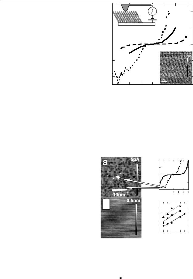
Figure 2. Current versus voltage for a conducting AFM probe in contact with a C13 alkanethiol monolayer on a gold electrode. The experimental arrangement is shown schematically in the inset on the upper left. The sample is submerged in toluene and maintained in a nitrogen environment. The curves are reversible and reproducible (long-dashed curve ‘1’) if the bias is kept below ±4 V at 14 nN contact force. Sweeping above this voltage leads to transient instability (short-dashed curve ‘2’) followed within 0.5 s by stable and reversible enhanced conductivity (solid curve ‘3’). The molecular lattice is shown in the AFM current image taken at 3 V bias and 1 nN contact force in the inset at the lower right.
|
(c) |
|
1 |
|
(a) |
(nA) |
|
||
0 |
.5 |
|||
|
||||
|
|
|||
|
urrent |
|
0 |
|
|
|
|||
|
|
|
||
|
C |
-0 |
.5 |
|
|
|
|
-1 

 -3 -2 -1
|
|
|
|
Bias (V) |
|
|
(d ) |
7 |
|
|
|
(b) |
|
|
|
|
|
(V) |
|
|
|
6nN |
|
|
6 |
|
|
||
|
Bias |
|
|
|
8nN |
|
5 |
|
|
|
|
|
ritical |
|
|
|
|
|
3 |
|
|
|
|
|
|
4 |
|
|
14nN |
|
|
|
|
|
|
|
C |
|
|
|
|
|
|
2 |
|
|
|
|
|
7 |
8 |
9 |
10 11 12 13 14 |
Chain Length (Carbons)
Figure 3. (a) Current and (b) topographical images of a C12 film that was pulsed above 4 V at a point near the centre of the image. The subsequent topographical scan (b) is flat, but the current image (a) shows a region of enhanced conductivity. Part (c) shows current versus voltage data taken on the unperturbed film (solid curve) and over the modified spot (dashed curve). Part (d) shows a plot of the critical bias required to switch to the enhanced conductivity mode as a function of alkane chain length and contact force ( 6 nN, 8 nN, •14 nN).
8

Making electrical contacts to molecular monolayers
(a)
Normalized Current
100
10
C8  C10
C10
1 |
C12 |
0.1
0.01
0.001
-5 |
0 |
5 |
10 |
15 |
20 |
Force (nN)
(b)
Current (nA)
20
15
86nm
10
5
0
0 |
5 |
10 |
15 |
Force (nN)
Figure 4. (a) The logarithm of the current as a function of contact force. Data are taken at +1 V substrate bias and have been normalized to unity at 5 nN in order to show plots for several chain lengths on one plot. Data are for C8 (×), C10 ( ) and C12 (♦). There are two distinct regions of approximately exponential behaviour, below and above 5 nN. At this force, the film is under a stress of about 1 GPa (tip radius = 10 nm). (b) Linear plot of current versus force for C8 fitted to the compression model described in the text (solid curve). The inset shows a TEM image of a typical gold-coated tip with an end radius of about 10 nm (the scale bar is 86 nm).
is logarithmic and the data show that there are two regions of roughly exponential current rise, one below and the other above a contact force of 5 nN (corresponding to a stress of about 1 GPa, see below). This first break was not evident in the work of Wold and Frisbie [29] and they state that they were not able to examine the low stress region in detail because of the adhesion of the tip to the monolayer. This problem was not present in this work in a fluid medium. They observed [29] a second break near 10 GPa, beyond the range of forces explored in the present work. In the region where our data overlap with those of Wold and Frisbie, the exponential scaling of the current is remarkably similar.
Some plausible reasons for the effect of contact force are:
(a) compression of the film, resulting in increased chain-to- chain tunnelling [29] (see below); (b) changes in the contact region itself and (c) changes in the electronic properties [38,39] as a result of deformation [40]. The tunnelling model has been discussed qualitatively by Wold and Frisbie [29] and we develop it quantitatively here.
Before doing so, it is important to clarify the difference between through-bond and chain-to-chain tunnelling. Slowinski et al [17] have shown that there are two components of tunnelling through alkanethiol monolayers. One is the chain-to- chain component (for which β ≈ 1.3 Å−1) and this depends on the film thickness, the electrons passing across the film by means of states located on neighbouring chains lying in the shortest direct path for tunnelling. The other is a through-bond tunnelling (for which β ≈ 0.9 Å−1 or 1.14 per methylene). In this case, the electrons pass along the backbone of the alkane chains. Since most of the deformation is taken up by the tilting of the molecules [40]), this rate is independent of the chain tilt with respect to the substrate, and therefore constant for a given chain length [17]. Thus, tunnelling that depends on film thickness must be dominated by the chain-to-chain process.
Deformation of the film may be characterized using the Hertzian model [41] which describes a spherical tip of radius R indenting into a uniform elastic film. The contact radius, r, depends on force, F , according to
|
|
|
|
|
|
|
|
F R |
1/3 |
|
|
||
|
|
|
|
r = |
|
|
. |
(3) |
|||||
|
|
|
|
K |
|||||||||
K is an effective modulus given by |
|
||||||||||||
K |
− |
1 |
= |
|
3 |
|
1 − ν12 |
|
+ |
1 − ν22 |
|
||
|
4 |
|
|
||||||||||
|
|
|
E1 |
|
E2 |
||||||||
where E1 is Young’s modulus for the monolayer (1010 N m−2 [42]) and E2 is the modulus for the tip (1.7×10¹¹ N m−2 [41]). ν1 and ν2 are Poisson’s ratios for the two materials, and we assume these to be 0.33. This leads to K = 1.4 ×10¹⁰ N m−2. The effective spring constant of the film is given by Kr so that the deformation, δz, is given by F/Kr or
δz = |
F 2/3 |
(4) |
K2/3R1/3 . |
The tunnelling current is proportional to the contact area multiplied by exp −β(z − δz) so that its force dependence is given by
i F 2/3 exp[CF 2/3] |
where C = |
K2/3R1/3 |
. (5) |
|
|
|
|
β |
|
As discussed above, the through-bond tunnelling is not expected to change as the film is compressed. For chain-to- chain tunnelling Slowinski et al [17] have shown that β ≈ 1.3 Å−1. Fits to the data for C8 are shown in figure 4(b). These fits yield C = 0.91 ± 0.2 × 10⁶ N2/3 below 5 nN and 0.23 ± 0.1 × 10⁶ N2/3 above 5 nN. Similar fits for the other chain lengths (not shown) yield C = 0.81 ± 0.2 × 10⁶ N2/3 (low force) and 0.22 ± 0.1 × 10⁶ N2/3 (high force) for C10 and C = 1.2 ±0.2 ×10⁶ N2/3 (low force) and 0.1 ±0.1 ×10⁶ N2/3 (high force) for C12. Thus, the films have a common force dependence corresponding to C ≈ 1 × 10⁶ N2/3 for forces below 5 nN. To see if this is reasonable, we take βS = 1.3 Å−1 [17] and K = 1.4 × 10¹⁰ N m−2 and use equation (5) to calculate R ≈ 10 nm. The inset in figure 4(b) shows an
9

X D Cui et al
|
0.1 |
|
|
|
|
|
|
|
|
1.4 |
|
|
|
|
|
|
|
|
|
|
|
(nA) |
|
|
|
|
8nN βN=1.1 |
|
|
|
1.2 |
|
0.01 |
|
|
|
|
|
|
|
|||
per molecule |
|
|
|
|
|
14nN βN=1.2 |
|
1 |
||
|
|
|
|
|
|
|
||||
0.001 |
|
|
|
|
|
|
|
Beta |
0.8 |
|
|
|
|
|
|
|
|
|
|||
|
|
6nN βN=1.0 |
|
|
|
0.6 |
||||
Current |
|
|
|
|
|
|
|
|||
0.0001 |
|
|
|
|
|
|
|
|
0.4 |
|
|
|
4.5nN βN=0.8 |
|
|
|
|
0.2 |
|||
|
|
|
|
|
|
|
|
|
|
|
|
10-5 |
|
|
|
|
|
|
|
5 |
0 |
|
7 |
8 |
9 |
10 |
11 |
12 |
13 |
1 |
||
|
|
|||||||||
Number of Carbons
|
|
|
|
Non-Resonant |
|
|
|
|
|
|
|
|
Resonant |
|
|
|
|
-4 |
-3 |
-2 |
-1 |
0 |
1 |
2 |
3 |
4 |
Substrate Bias (V)
Figure 5. Logarithmic plot of current versus alkane chain length for 4.5 nN ( ), 6 nN ( ), 8 nN (♦) and 14 nN (•) contact force. The solid lines are fits to exponentials yielding βN = 0.8, 1.0, 1.1 and 1.2, respectively. The data points have been corrected for the changing contact area using the contact radius calculated from equation (3). Using an area per molecule of 0.22 nm−2 and a probe radius of 10 nm yields the following number of molecules contacted: 4.5 nN, 32; 6 nN, 38; 8 nN, 46; 12 nN, 56; and 14 nN, 66. The measured currents were divided by these numbers to yield the current per molecule.
SEM image of a typical metal-coated probe, and it is clear that its end radius is indeed about 10 nm.
The initial contact pressure at the onset of current measurement (figure 4(a)) is of the order of 100 MPa, leading one to question the appropriateness of the value of Young’s modulus we have used here [42]. These measurements were made using a nanoindenter on LB multilayers. A comparison of our figure 3(a) with figure 4 of the paper by Son et al [28] (where current was acquired at stresses as low as 20 MPa) shows that the current increases about one hundredfold for a three times increase of force (or stress) in both sets of experiments, implying that the elastic properties of the monolayer were the same in the two experiments. Another check comes from comparing the values for β from the two experiments, and these do not differ greatly. Thus, our use of the Weihs data [42] for Young’s modulus does not appear to be unreasonable, implying that the initial force dependence is well explained by elastic deformation of the film thickness leading to a change in chain-to-chain tunnelling.
If the tip radius remains reasonably constant over the force range, the change above 5 nN must correspond to a change in the mechanical properties of the monolayers. For these tips, 5 nN corresponds to a film stress of about 1 GPa (calculated from the force with the contact area estimated using r from equation (3)), a stress at which changes in the elastic properties of alkanethiol SAMs have been observed [43]. Data in this region were fitted by increasing the modulus appropriately. Note that the deformation becomes quite dependent on chain length in these highly distorted films, and this will have an effect on measurements of β based on measurements of different chain lengths.
In summary, our data are consistent with the results of Wold and Frisbie [29] and quantitatively accounted for by film deformation, confirming their proposal [29] that chain-to- chain tunnelling is altered by compression of the monolayer.
Figure 6. Calculated and measured values for βN as a function of bias. The data are for 4.5 nN (+), 6 nN (•), 8 nN ( ), 12 nN ( ) and 14 nN ( ) contact force. Representative error bars have been shown on some of the 4.5 nN and 14 nN data and data have been suppressed near zero bias where the error is of the order of the data values. Extrapolation of the 14, 12, 8 and 6 nN currents to zero force using equation (5) yields the points shown as large open circles. The two curves are (dashed) for off-resonance and (solid) near resonance calculations as described in the text.
4.3. Determination of the electronic decay constant
The previous discussion shows that, provided contact forces and applied biases remain below critical values, reproducible values of current should be obtained at a given contact force and bias, as long as corrections are made for differential film compressibilities above about 1 GPa stress. In practice, we find considerable run-to-run variation, presumably because of variations in the AFM probes themselves and because of variable contamination in the contact region. Nonetheless, the overall variation is small compared to the change in conductivity that occurs as the chain length is varied. This is shown in figure 5 where current measurements taken at a substrate bias of +2.5 V are plotted for a number of contact forces as a function of the alkane chain length. The data have been normalized for the change of contact area, as explained in the figure caption, yielding a nominal ‘current per molecule’. The mean currents and their associated standard deviations were obtained from curves taken from a minimum of six and a maximum of 20 different runs using different tips and samples. In the worst case, the standard deviation on a current datum is still less than the change resulting from the addition of two carbon atoms to the chain. The current decays exponentially with chain length at each force and the corresponding values of βN are similar, spanning 0.8 per methylene (4.5 nN) to 1.2 per metheylene (14 nN). The change in βN with force is qualitatively consistent with the length dependence of the film compression at high forces shown in figure 4(a). Shorter films are compressed more in this high-force region and this leads to a greater change of current with chain length. The extra decay of current with increasing chain length translates into an apparently larger value for β.
Values of βN as a function of both force and bias are displayed in figure 6. Some representative error bars are shown for the highest and lowest forces used (some data near the
10

Making electrical contacts to molecular monolayers
Current (nA)
Current (nA)
1.5 |
(a) |
||||
1 |
C8 |
||||
0.5 |
|
|
|
|
|
0 |
0.01 |
|
|
|
|
|
|
|
|
||
-0.5 |
0 |
|
|
|
|
|
|
|
|
||
-1 |
-0.01 |
|
|
|
|
-0.5 0 0.5 |
|||||
-1.5 |
|
|
|
|
|
|
|
|
|
|
|
-3 -2 -1 0 1 2 3 Tip Bias (V)
0.3 |
|
|
|
|
|
|
(c) |
|
|
|
|
|
|
0.2 |
C10 |
|
|
|
||
0.1 |
|
|
|
|
||
0 |
|
|
|
|
|
|
-0.1 |
|
0.001 |
|
|
|
|
|
0 |
|
|
|
|
|
-0.2 |
|
|
|
|
|
|
|
-0.001 |
|
|
|
|
|
|
|
|
|
|
|
|
-0.3 |
|
-0.5 |
0 |
0.5 |
||
|
|
|
|
|
|
|
-3 -2 -1 |
0 1 |
2 |
3 |
|||
Tip Bias (V)
|
0.01 |
|
|
|
|
|
|
|
|
|
(nA) |
|
|
(b) |
|
|
|
|
|
||
|
|
|
|
|
|
|
|
|||
|
|
|
|
|
|
|
|
|
|
|
Current |
0 |
|
|
|
|
|
|
|
|
|
|
|
|
|
|
|
|
|
|
|
|
|
-0.01 |
|
|
|
|
|
|
|
|
|
|
|
|
|
|
|
|
|
|
|
|
|
-1 |
0 |
1 |
|
||||||
|
|
|
|
|
|
Tip Bias (V) |
||||
|
0.02 |
|
|
|
|
|
|
|
|
|
|
|
|
|
|
|
|
|
|
|
|
(nA) |
|
|
|
(d ) |
|
C10 |
|
|
|
|
|
|
|
|
|
|
|
|
|
||
|
|
|
|
|
|
|
|
|
|
|
Current |
0 |
|
|
|
|
|
|
|
|
|
|
|
|
|
|
|
|
|
|
|
|
|
-0.02 |
|
|
|
|
|
|
|
|
|
|
|
|
|
|
|
|
||||
|
|
|
|
|
|
|
|
|
|
|
|
-1 |
0 |
1 |
|
||||||
Tip Bias (V)
Figure 7. A sample of I –V curves for C8 ((a) and (b)) and C10 ((c) and (d)) alkanethiol SAMs. The dots represent data measured at 6 nN contact force and the solid lines are fits to the Simmons formula (equation (6)). In the full voltage range ((a) and (c)) the data are badly fitted in that the real ‘turn on’ of the current is much sharper than these fits. This is illustrated by the insets in (a) and (c) that show the data and fit in the region between ±0.5 V. The attempt to fit the high current tails of the data yields too small a conductivity at low bias. The Simmons formula fits very well over a ±1.5 V range ((b) and (d)), yielding an effective barrier height of 2.3 V in both cases.
lowest biases have been suppressed because the uncertainty in this region exceeds the mean values). The slight decrease of βN with decreasing bias may be significant but it is smaller than the experimental uncertainties. The lines show the results of model calculations and will be discussed in a later section.
The spread owing to changes in contact force is clear, and raises the question of the correct procedure for deducing a value of βN corresponding to ‘zero’ contact force. The data in figure 4(a) suggest a simple procedure. Below 5 nN, the force dependence of the current does not appear to depend strongly on alkane chain length, so these data should be free of the artifact caused by chain-length dependent distortion at higher forces. On the other hand, the data taken at lower force are significantly noisier, so these data alone do not yield reliable values for βN . We have used equation (5) and the exponents derived earlier to extrapolate each data set to zero force and then used the corrected data to calculate βN (V ). These calculated values are shown as large open circles in figure 6. They overlap the 4.5 nN data quite well, showing that this extrapolation is valid within the uncertainties.
Thus, the small force dependence of βN is successfully accounted for by differential mechanical deformations of the monolayers. This suggests that the electronic properties of the film do not change strongly with contact force, even under the large contact pressures used here. This also means that the contact, once made, cannot change its properties much as further force is applied, because the changes appear to be well accounted for by deformation alone.
Thus we will use the data obtained from this extrapolation to zero force as the ‘true’ results for βN . It is approximately constant over the range of measurement (though uncertainties near zero bias are very large). Excluding data below ±0.7 V and averaging yields a value of βN = 0.8 ± 0.2 per methylene. This is in good agreement with electrochemical electron transfer studies [16–18] and measurements made with mercury-drop contacts [23]. It is a little smaller than the values determined by STM [7] or conducting AFM [15, 27, 29] but these other studies were not corrected for the effects of contact force in the manner described here.
4.4. I –V characteristics and comparison with theories
We turn here to an examination of the I –V curves. Figure 7 shows representative curves from a number of films obtained at 6 nN contact force. In order to compare these to what is expected for a simple tunnelling process, we have made comparisons to a simple model for tunnelling through a planar barrier [44] and to first-principles calculations we have carried out as described in the theoretical introduction.
The Simmons model [44] yields the following results for the current density, J , as a function of bias
|
|
|
6.2 × 10⁻⁷ |
|
|
|
|
|
|
|
|
|
|
|
|
|
|
J |
= |
|
(φ |
|
− |
V /2) exp |
− |
1.025s |
|
|
φ |
0 − |
V /2 |
|
|||
s2 |
|
||||||||||||||||
|
|
|
0 |
|
|
|
|
||||||||||
|
|
−(φ0 + V /2) exp |
− 1.025s |
φ0 + V /2 |
A m−2 |
(6) |
|||||||||||
11

X D Cui et al
where s, φ0 and V are the spacing between the two electrodes (in Å), energy gap between the Fermi energy and a band-edge (in eV) and bias (in V) respectively. The measured data points were fitted using s, φ0 and the overall current scale as free parameters. The results of these fits are shown as the solid lines in figures 7(a) and (c). Values for s (1.2 nm) and φ0 (2.4 eV for C8 and 2.7 eV for C10) were of the same order of magnitude as the known film thickness and the work function of gold. The fits reproduce the gross features of the experimental data quite well, but a more careful examination reveals a problem. The experimentally observed ‘turn-on’ in the high current region is much more abrupt than predicted by the Simmons theory. This is particularly evident when the low bias region is magnified as shown in the insets in figures 7(a) and (c). The Simmons formula predicts much more conductivity at low bias than is actually observed. At first sight, this observation appears to be at variance with the work of Wold and Frisbie [29]. However, when we fit our data over the ±1.5 V range of their data (figures 7(b) and (d)) good fits are obtained with a barrier height of 2.3 eV and s = 1.3 nm, essentially identical to their result.
We can treat the high-voltage region more precisely with a first-principles simulation. These same simulations can be used to predict values for βN . Two adjustable parameters are required: one is the overall scale of the current, the other is the energy difference, φ0, between the Fermi energy of the metal electrodes and the nearest molecular orbital of the molecule (the Simmons theory corresponds to large φ0). The dashed curve in figure 8 shows a simulated I –V curve for φ0 = 2.7 eV from the HOMO of the alkane system for a C10 alkanethiol. This position was chosen because approaching the HOMO more closely (see below) improved the fit more than approaching the LUMO. The best fit to the data (dots) obtained by scaling the current is poor (dashed curve). This is again obvious in the low bias region shown in the inset. However, in line with the predictions of the simple model (equation (1)) this value for φ0 leads to a βN (V ) that is nearly constant, in good agreement with our measurements (dashed curve in figure 6). In this model, the molecule is far from resonance over the entire range of bias so βN remains nearly constant. If φ0 is adjusted for a best fit to the I –V data (solid curve in figure 8 and also in the inset) excellent agreement can be obtained with φ0 = 1.7 eV. This is close to resonance at the higher biases, and the improved agreement results from the rapid rise in current as bias is increased. However, this also implies a strong voltage dependence for βN . The calculated values of βN (V ) for this near-resonant case are shown by the solid curve in figure 6, and it is clear that they disagree with the experimental data.
Something clearly changes in the experiment in the larger bias region, causing the observed disagreement with theory. It is unlikely to be the alkane molecule itself, because βN (V ) is relatively constant between 1.5 and 3 V. This suggests that the problem may lie with the contacts to the monolayer.
Another reason for suspecting a contact problem lies with the absolute scale of current. It has been adjusted for best fits in order to compare the shape of the curves, obscuring the fact that the absolute values of the calculated currents are many orders of magnitude higher than the measured values. This adds to the motivation for making a direct test of the effects of the top contact.
|
0.001 |
|
|
|
|
|
|
0.0005 |
Non-Resonant |
|
|
|
|
|
|
|
|
|
|
|
(nA) |
0 |
|
|
|
|
|
Current |
|
|
|
|
|
|
-0.0005 |
|
|
|
|
|
|
|
|
|
|
|
|
|
|
Resonant |
|
|
|
|
|
|
-0.001 |
|
|
|
|
|
|
-0.0015 |
|
|
|
|
|
|
-4 -3 -2 -1 |
0 |
1 |
2 |
3 |
4 |
Substrate Bias (V)
Figure 8. Current per molecule (dots) for C10 at a contact force of 5 nN. The theory curves were calculated as described in the text and scaled for overall best fit to the data. In addition to this scaling, the other adjustable parameter is the energy difference between the Fermi energy and an alkane HOMO. This is adjusted to give the best overall fit (solid curve labelled ‘resonant’) and then moved further away from resonance (dashed curve labelled ‘non-resonant’). The near-resonant case is a better fit, both at high current and (see inset showing magnified data) near zero bias. The same theory has been used to calculate βN (V ) for these two cases and corresponding curves are shown in figure 5. The best fit to the current–voltage data fails to fit the measured βN (V ).
4.5. Testing the contacts—a gold tip bonded to a dithiolated film
The contact has been shown to be an important factor in measuring the electrical properties of carbon nanotubes [45]. We have shown that the surfaces of alkanethiol monolayers can charge on contact [37], an indication of strange electronic properties. A straightforward way to better define the top contact is to chemisorb the top end of the monolayer as well as the bottom end.
We have taken current–voltage data from 1,8-octanedithiol monolayers. There is some evidence that they pack vertically on a gold substrate with one thiol group exposed on the surface [46]. We have experimented extensively with deposition conditions, and while ellipsometry shows that monolayers are formed, STM images suggest that they are usually quite disordered, although ordered regions were found on occasion. In some cases these had molecular spacings consistent with the proposed upright placement of the alkanedithiol. In many cases the measured spacings were not consistent with this model.
The poor quality of the films precludes systematic interpretation of their electronic properties, but some striking effects were observed nonetheless. Consistent with the heterogeneity of the STM images, we observed three types of I –V curve using a conducting AFM with a gold-coated probe. One type, often seen on first contact, was similar to the curves obtained from alkanethiol monolayers and was very sensitive to contact force. The two other types of curve were both remarkably insensitive to the contact force, and were obtained only when force curves showed large hysteresis associated with formation of bonds to the top contact. The ‘bonded’ I –V curves were observed for several different experiments using fifteen different tips on eleven different samples. A low current
12

|
6 |
|
|
|
|
|
|
|
|
|
|
|
|
|
|
|
|
|
|
|
|
|
|
|
|
(a) |
|
|
|
|
|
|
|
|
|
|
|
|
|
|
|
|
|
||
|
4 |
|
|
|
|
|
|
|
F=6nN |
|
|
|
|
|
|
|
|
|||||
|
|
|
|
|
|
|
|
|
|
|
|
|
|
|
|
|
|
|
||||
|
|
|
|
|
|
|
|
|
|
|
F=2nN |
|
|
|
|
|
|
|
|
|||
|
|
|
|
|
|
|
|
|
|
|
|
|
|
|
|
|
|
|
||||
|
|
|
|
|
|
|
|
|
|
|
|
|
|
|
|
|
|
|
|
|||
(nA) |
|
|
|
|
|
|
|
|
|
|
|
F=11nN |
|
|
|
|
|
|
|
|||
2 |
|
|
|
|
|
|
|
|
|
|
F=18nN |
|
|
|
|
|
|
|
||||
Current |
|
|
|
|
|
|
|
|
|
|
F=-3nN |
|
|
|
|
|
|
|
||||
0 |
|
|
|
|
|
|
|
|
|
|
|
|
|
|
|
|
|
|||||
|
-2 |
|
|
|
|
|
|
|
|
|
|
|
|
|
|
|
|
|
|
|
|
|
|
|
|
|
|
|
|
|
|
|
|
|
|
|
|
|
|
|
|
|
|
|
|
|
-4 |
|
|
|
|
|
|
|
|
|
|
|
|
|
|
|
|
|
|
|
|
|
|
|
|
|
|
|
|
|
|
|
|
|
|
|
|
|
|
|
|
|
|
|
|
|
|
|
|
|
|
|
|
|
|
|
|
|
|
|
|
|
|
|
|
|
|
|
|
-3 |
-2 |
-1 |
|
|
|
|
|
|
|
|
|
|
|
|
|
|
|||||
|
|
|
|
|
|
|
|
Tip Bias (V) |
|
|
|
|
|
|
|
|
||||||
|
100 |
|
|
|
|
|
|
|
|
|
|
|
|
|
|
|
|
|
|
|
|
|
|
|
|
(b) |
|
|
|
|
|
|
|
|
|
|
|
|
|
|
|
|
|
||
(nA) |
50 |
|
|
|
|
|
|
|
|
|
|
|
|
|
|
|
|
|
|
|
|
|
|
|
|
|
|
|
|
|
|
|
|
|
|
|
|
|
|
|
|
|
|
||
|
|
|
|
|
|
|
|
|
|
|
|
|
|
|
|
|
|
|
|
|
|
|
Current |
0 |
|
|
|
|
|
|
|
|
|
|
|
|
|
|
|
|
|
|
|
|
|
|
|
|
|
|
|
|
|
|
|
|
|
|
|
|
|
|
|
|
|
|
|
|
|
|
|
|
|
|
|
|
|
|
|
|
|
|
|
|
|
|
|
|
|
|
|
|
-50 |
|
|
|
|
|
|
|
|
|
|
|
|
|
F=6nN |
|
|
|
|
|||
|
|
|
|
|
|
|
|
|
|
|
|
|
|
F=8nN |
|
|
|
|
||||
|
|
|
|
|
|
|
|
|
|
|
|
|
|
|
|
|
|
|
||||
|
|
|
|
|
|
|
|
|
|
|
|
|
|
|
F=14nN |
|
|
|
|
|||
|
-100 |
|
|
|
|
|
|
|
|
|
|
|
|
|
|
|
|
|
|
|
|
|
|
|
|
|
|
|
|
|
|
|
|
|
|
|
|
|
|
|
|
|
|
|
|
|
|
|
|
|
|
|
|
|
|
|
|
|
|
|
|
|
|
|
|
|
|
|
|
|
|
|
|
|
|
|
|
|
|
|
|
|
|
|
|
|
|
|
|
|
|
|
-4 |
-3 |
|
-2 -1 0 |
1 |
2 |
|
3 |
4 |
|||||||||||||
Tip Bias (V)
Figure 9. I –V data for C8 alkanedithiol monolayers on Au(111) contacted with an Au-coated tip at a number of contact forces, as labelled. The monolayers were rather disordered (see text) but the tip adhered strongly to the films as evidenced by features in the force curves on retraction. Two types of force curves were obtained frequently, with currents somewhat higher than observed in the corresponding alkanethiol monolayers (a) and very much higher (b). In each case, the curves showed a remarkable insensitivity to contact force—in most cases the data taken at different forces overlap. The curve labelled ‘−3 nN’ corresponds to a film under tension. The small discontinuity near +2 V in (a) is caused by the log/linear amplifier calibration procedure as described in the experimental details.
family (figure 9(a)) is characterized by an average current at
±3 V of 4.6 nA with a standard deviation of 0.7 nA (n = 136), and a high current family (figure 9(b)) is characterized by an average current at ±3 V of 46 nA with a standard deviation of 6 nA (n = 80).
The lack of force dependence is quite striking. The curves shown in figure 9 show data taken in nominal tension (F = −3 nN, figure 9(a)) up to a very large stress (18 nN), well into the region where the film is distorted significantly. Yet data for both the low current curves (figure 9(a)) and the high current curves (figure 9(b)) are remarkably insensitive to contact force. This remarkable change when measurements are made on alkanedithiol films is further support for the notion that the tip- to-molecule contact plays a critical role in charge transport. It appears as though the change to chemically bonded contacts has changed the dominant transport mode from chain-to-chain to through-bond.
Making electrical contacts to molecular monolayers
5. Conclusions
Alkanethiol monolayers change properties in a non-reversible way when subject to high electric fields and mechanical compression, and this breakdown occurs at a higher field in a controlled environment compared to ambient air. The breakdown may be caused by the removal of a small number of molecules by voltage pulses [36].
The effect of contact force on tunnelling through molecular films depends strongly on the nature of the contact between the metal and the molecule. With physical contact, the tunnelling rate is very sensitive to distortion of the film thickness. The dependence of current on contact force is well accounted for by a chain-to-chain electronic decay coefficient of about 1 Å−1 and the known tip radius and Young’s modulus of the monolayers below a stress of 1 GPa. The elastic properties of the film appear to change in a way that depends on chain length at high loading, an artifact that can be corrected for when calculating βN . Taking account of this effect, we conclude that βN = 0.8 ± 0.2, and is essentially constant over the ±3 V range of bias studied here and consistent with the result of Wold and Frisbie [29].
The I –V characteristics of mechanically contacted monolayers cannot be accounted for by tunnelling theory over the full ±3 V range studied in this work. In order to fit both the high-voltage region (where current grows exponentially) and the low-voltage (ohmic) region, the theory must be adjusted so that the electrons approach resonance with alkane orbitals at the higher bias. Yet such resonant tunnelling implies a rapid change of βN as resonance is approached, and this is not observed. Simple tunnelling theory works well for biases below ±1.5 V (Wold and Frisbie [29] and see figure 7) so this suggests that some property of the tunnel junction changes above this voltage. The relatively constant value of βN (V ) over the entire ±3 V range implies that the change does not occur in the alkane chain itself, because a change in the mode of charge transport would be likely to result in a change in the effective value of βN . An alternative explanation is that the contacts themselves change as the bias is increased. That is, rather than an abrupt change in the molecule itself (unlikely, given the data for βN (V )), a sharp ‘turn-on’ of current occurs because of electric breakdown in the contact regions.
The important role of the contact is illustrated by I –V curves obtained from alkanedithiol monolayers. Where there is evidence of bonding between the probe and the top thiol groups in the force curve, the tunnelling rate becomes essentially independent of contact force. We expect that considerable insight will be gained when single dithiol molecules are bonded between a gold tip and a gold substrate in a well-defined geometry. In particular, the scaling factors used to make theory and experiment agree (figure 8) are very large indeed (four or more orders of magnitude). Efforts to construct a well-defined single molecule system are the focus of current research, in the hope that they will shed some light on this, and other problems.
Acknowledgments
We thank Eloy Perez for suggesting a study of n-alkanes, Jack Houston for useful discussions and Dan Frisbie for
13

X D Cui et al
commenting on our manuscript. Support was received from the NSF (DBI-951-3233, DMR-9632635 and CHE 0078835).
References
[1]Reed M A, Zhou C, Muller C J, Burgin T P and Tour J M 1997
Science 278 252–4
[2]Metzger R M 1999 Acc. Chem. Res. 32 950–7
[3]Burghard M, Fischer C M, Roth S, Schlick U and Hanack M 1996 Synth. Met. 76 241–4
[4]Wohlfart P, Weiss J, Kashammer J, Winter C, Scheumann V, Fischer R A and Mittler-Neher S 1999 Thin Solid Films 340 274–9
[5]Chen J, Reed M A, Rawlett M A and Tour J M 1999 Science 286 1550–2
[6]Bumm L A, Arnold J J, Cygan M T, Dunbar T D, Burgin T P, Jones L, Allara D L, Tour J M and Weiss P S 1996 Science 271 1705–7
[7]Bumm L A, Arnold J J, Dunbar T D, Allara D L and Weiss P S 1999 J. Phys. Chem. 103 8122–7
[8]Datta S, Tian W, Hong S, Reifenberger R, Henderson J I and Kubiak C P 1997 Phys. Rev. Lett. 79 2530–3
[9]Tian W, Datta S, Hong S, Reifenberger R, Henderson J I and Kubiak C P 1998 J. Chem. Phys. 109 2874–82
[10]Tao N 1996 Phys. Rev. Lett. 76 4066–9
[11]Han W, Durantini E N, Moore T A, Moore A L, Gust D, Rez P, Leatherman G, Seely G R, Tao N and Lindsay S M 1997 J. Phys. Chem. 101 10 719–25
[12]Durig U, Zuger O, Michel B, Haussling L and Ringsdorf H 1993 Phys. Rev. B 48 1711–17
[13]Fan F R F, Yang J, Dirk S, Proce D W, Kosynkin D, Tour J M and Bard A J 2001 J. Am. Chem. Soc. 123 2452–5
[14]Leatherman G, Durantini E N, Gust D, Moore T A,
Moore A L, Stone S, Zhou Z, Rez P, Li Y Z and
Lindsay S M 1999 J. Phys. Chem. B 103 4006–10
[15]Wold D J and Frisbie C D 2000 J. Am. Chem. Soc. 122 2970–1
[16]Miller C, Cuendet P and Gratzel M 1991 J. Phys. Chem. 95 877–86
[17]Slowinski K, Chamberlain R V, Miller C J and Majda M 1997
J. Am. Chem. Soc. 119 11 910–19
[18]Chidsey C E D 1991 Science 251 919–22
[19]Smalley J N, Feldberg S W, Chidsey C E D, Linford M R, Newton M D and Liu Y P 1995 J. Phys. Chem. 99 13 141–9
[20]Becka A M and Miller C J 1992 J. Phys. Chem. 96 2657–68
[21]Hsu Y, Penner T L and Whitten D G 1992 J. Phys. Chem. 96 2790–5
[22]Gu Y and Waldeck D H 1998 J. Phys. Chem. B 102 9015–28
[23]Slowinski K, Fong H K Y and Majda M 1999 J. Am. Chem. Soc. 121 7257–61
[24]Holmlin E, Haag R, Chabinye M L, Ismagilov R F,
Cohen A E, Terfort A, Rampi M A and Whitesides G M 2001 J. Am. Chem. Soc. 123 5075–85
[25]Boulas C, Davidovits J V, Rondelez F and Vuillaume D 1996
Phys. Rev. Lett. 76 4797–800
[26]Rampi M, Schueller O A J and Whitesides G M 1998 Appl. Phys. Lett. 72 1781–3
[27]Salmeron M, Neubauer G, Folch A, Tomitori M, Ogletree D F and Sautet P 1993 Langmuir 9 3600–11
[28]Son K A, Kim H I and Houston J E 2001 Phys. Rev. Lett. 86 5357–60
[29]Wold D J and Frisbie C D 2001 J. Am. Chem. Soc. 123
5549–56
[30]Mujica V, Kemp M and Ratner M A 1994 J. Chem. Phys. 101 6849–55
[31]Demkov A A, Ortega J, Sankey O F and Grumbach M P 1995
Phys. Rev. B 52 1618
[32]Sankey O F, Demkov A A, Windl W, Fritsch J H, Lewis J P and Fuentes-Cabrera M 1998 Int. J. Quantum Chem. 69 327
[33]Economou E N 1983 Green Functions in Quantum Physics
(Berlin: Springer)
[34]Durig U, Novotny L and Michel B 1997 Rev. Sci. Instrum. 68 3814–16
[35]DeRose J A, Thundat T, Nagahara L A and Lindsay S M 1991
Surf. Sci. 256 102–8
[36]Mizutani W, Ishida T and Tokumoto H 1998 Langmuir 14 7197–202
[37]Cui X D, Zarate X, Tomfohr J, Primak A, Moore A L,
Moore T A, Gust D, Harris G, Sankey O F and Lindsay S M 2001 submitted
[38]Joachim C, Gimzewski J K, Schlittler R R and Chavy C 1995
Phys. Rev. Lett. 74 2102–5
[39]Lindsay S M, Sankey O F, Li Y and Herbst C 1990 J. Phys. Chem. 94 4655–60
[40]Siepmann J I and McDonald I R 1993 Phys. Rev. Lett. 70 453–6
[41]Burnham N A and Colton R J 1989 J. Vac. Sci. Technol. A 7 2906–13
[42]Weihs T P, Nawaz Z, Jarvis S P and Pethica J B 1991 Appl. Phys. Lett. 59 3536–8
[43]Houston J E 2001 Private communication
[44]Simmons J G 1963 J. Appl. Phys. 34 1793–803
[45]Frank S, Poncharal P, Wang Z L and de Heer W A 1998
Science 280 1744–6
[46]Yang J S, Lee C C, Yau S L, Chang C C, Lee C-C and Leu J M 2000 J. Org. Chem. 65 871–7
14