

2.3 Statik registers
A register is a collection of binary cells used to store a bit-vector. An n-bit register is shown in Figure 2.28. The data input and output are the n-bit vectors I and Q, respectively. The output of the register corresponds to its state. CK is the synchronizing clock. The control inputs are LOAD and CLEAR. If LOAD=1, the next state of the register is defined by the inputs present during the clock pulse; if LOAD=0 the state remains unchanged. That is,
![]()
The CLEAR input is asynchronous and serves to load a special state (0, 0 , . . . , 0) into the register. It is commonly used at the beginning of the system operation for initialization purposes. As discussed in Appendix C, the asynchronous inputs should not be used during the synchronous operation.
An implementation of a register using SR flip-flops is given in Figure 2.29. Three-state outputs may be provided in order to simplify the use of registers in larger networks. An additional control input, ENABLE, determines whether the register outputs correspond to the state of the cells or have third-state value (TS). A block diagram of a register with three-state outputs is shown in Figure 2.30.

Fig. 2.28 - Block representation of an n-bit register.

Fig. 2.29 - Implementation of an n-bit register.

Fig. 2.30 - n-bit register with three-state outputs.
2.4 Shift register Combinatorial shift register (barrel shifter)
For many arithmetic operations, a bit pattern must be shifted by one or more binary digits. This operation is usually carried out by a shift register, as described in Section 10.5. A single clock pulse results in a shift by one bit. There is a disadvantage, however, in that a sequential controller is necessary to organize loading of the bit pattern into the shift register and the subsequent shifting by a given number of binary digits.
The same operation may be carried out without recourse to clocked sequential control by employing instead a combinatorial network involving multiplexers, as illustrated in Fig. 2.32 For this reason, the unclocked shift registers The same operation may be carried out without recourse to clocked sequential control by employing instead a combinatorial network involving multiplexers, as illustrated in Fig. 2.32. For this reason, the unclocked shift registers involved are termed combinatorial or asynchronous shift registers. If, in Fig. 2.32, the address A = 0 is applied, then y3 = x3, y2 = x2 etc., but if A = 1, then y3 = x2, y2 = x1,
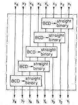
Fig . 2.31 - Block diagram of BCD-to-straight binary converter SN 74 S 484.
y1 = x0 and y0 = x -1 due to the wiring arrangement of the multiplexers. The bit pattern X therefore appears at the output left-shifted by one digit As with a normal shift register, the MSB is lost. If multiplexers with N inputs are used, a shift of 0, 1, 2 ... (N — 1) bits can be executed. For the example in Fig. 2.32, N = 4; the corresponding function table is shown in Fig. 2.33.

Fig. 2.32 - Barrel shifter made up of multiplexers.
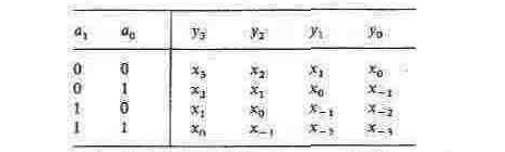
Fig. 2.33 - Function table of the barrel shifter.
If the loss of MSBs is to be avoided, the shift register may be extended by adding identical elements, as illustrated in Fig. 2.34. For the chosen example, where N = 4, a 5-bit number X can be shifted in this way by a maximum of 3 bits without loss of information. The shifted number then appears at outputs y3 to y7.

Fig. 2.34- Extended barrel shifter.
 The circuit in Fig.
2.34 can also be operated as a ring
shifter if the extension inputs
x-1
to x–3
is
connected to inputs x1
to x3,
as in Fig.
2.35.
The circuit in Fig.
2.34 can also be operated as a ring
shifter if the extension inputs
x-1
to x–3
is
connected to inputs x1
to x3,
as in Fig.
2.35.
Fig. 2.35 - Ring shifter.
1C types:
4 bit (TTL): Am 25 S 10 from AMD
16bit(TTL): SN 74 AS 897 from Texas Instruments
32 bit (CMOS): LSH32 from Logic Devices.