

Priority Encoders
The encoders discussed previously have the limitation that only one input can have the value 1 at a given time. In a priority encoder, many inputs can have the value 1 and the output represents the highest-priority input. There is a fixed priority ordering implemented in the encoder. Usually, x0 is of lowest priority and of highest priority. An enable input Ein and the outputs Eout and A are required to build larger priority encoders.
A high-level description is
y= |
i if xi=1 and (xk=0, k>i) Ein=1 |
0 otherwise |
where
and
Eout= |
1 if (for all i, xi=0) and Ein=1 |
0 otherwise |
And
A= |
1 if (at least one xi=1) and Ein=1 |
0 otherwise |
A priority encoder is used to select one of a set of events that can occur simultaneously and to represent this event by an integer that identifies it.

Fig. 1.32 - Priority encoder.
A priority encoder can be implemented by two subsystems, as indicated in Figure 1.32. The first subsystem, a priority-resolution network, removes all 1's except the highest priority 1; the second subsystem is a binary encoder.
The priority resolution system has 2n
inputs (x0
to
)
and 2n
outputs (z0
to
![]() ).
).
Its high-level description is:
zi= |
1 if xi=1 and (xk=0, k>i) |
0 otherwise |
This corresponds to the switching expressions
![]()
The priority resolution system can be implemented directly by AND gates of (2i –1) inputs or by an iterative network as discussed in Section 4.5. An implementation of a 4-input priority resolution network using AND gates is illustrated in Figure 1.33.
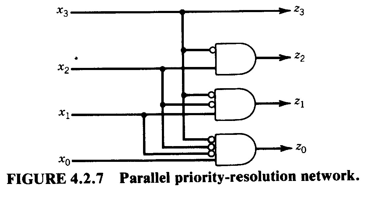
Fig. 1.33 - Parallel priority-resolution network.
1.6 Multiplexers (Selectors)
The opposite of a demultiplexer is a multiplexer. Starting from the circuit in Fig. 1.43, it can be implemented by swapping the outputs and input to give the basic circuit in Fig. 1.34. This provides a particularly simple illustration of the mode of operation: a 1-out-of-n decoder selects from n inputs the one whose number coincides with the number entered and switches it to the. output. The corresponding gate implementation is shown in Fig. 1.35.

Fig. 1.34 - Basic multiplexer operation. Fig. 1.35 - Multiplexer circuit.
![]()
In CMOS technology, a multiplexer can be implemented using both gates and analog switches (transmission gates). When analog switches are employed, signal transmission is bidirectional. In this case, therefore, the multiplexer is identical to the demultiplexer, as comparison of Figs. 1.34 will show. The circuit is then known as an analog multiplexer/demultiplexer.
 The or operation required in multiplexers
can also be implemented using a wired-OR connection. This possibility
is shown for open-collector outputs in
Fig. 1.36. In positive logic, this
connection results in an and
operation, it is necessary
to resort to the complemented signals .
The or operation required in multiplexers
can also be implemented using a wired-OR connection. This possibility
is shown for open-collector outputs in
Fig. 1.36. In positive logic, this
connection results in an and
operation, it is necessary
to resort to the complemented signals .
Fig. 1.36 - Multiplexer with open-collector gates. Fig. 1.37 - Multiplexer with tristate gates.
In order to overcome the disadvantage associated with open-collector outputs, namely the higher switching time, Instate outputs can be connected in parallel, with only one being activated at a time. This alternative is shown in Fig. 1.37.
Although the possible implementations of the or operation shown in Figs. 1.36 and 1.37 are not employed in integrated multiplexers, they are useful if the signal sources of the multiplexer are spatially distributed. Arrangements of this kind are found in bus systems, as we shall describe in Chapter 21.
Some commonly used multiplexers are listed in Fig. 1.38.
-
Inputs
TTL
ECL
CMOS
digital
CMOS analog
16
74LS150
4515
4067
2x8
74LS4511
4097
8
74LS151
10164
4512
4051
4x4
74LS4531
2x4
74LS153
10174
4539
4052
8x2
74LS604
4x2
74LS157
10159
4519
4066
1 Manufacturer: MMI
Fig. 1.38 - Integrated multiplexers. "CMOS analog" means multiplexer/demultiplexer with transmission gate.
A 2n-input multiplexer is a combinational system with n control (select) inputs s = (sn-1, . . . , s0), 2n data inputs x = ( , . . , x0), a module enable E, and one data output y (Figure1.39). The values of the control variables s are interpreted as the binary representation of an integer from 0 to 2n -1. The output y corresponds to data input xi, if s represents the integer i.

Fig. 1.39 - 2-input multiplexer.
A high-level description is.
y= |
xs if E= 1 |
0 if E=0 |
where
![]()
In the description of systems, this module is denoted as
y = MUX(x, s, E)
For example, MUX((1,0,1,1), (1,0), 1) = 0.
The switching expression representing the multiplexer is
![]()
where mi(s) is the ith minterm of the n select variables.
A vector multiplexer is a generalized multiplexer in which each of the data inputs the output are k-bit vectors. A block diagram is shown in Figure 1.40. A multiplexer is used whenever one of several objects has to be selected for transmission or as input to some combinational system.
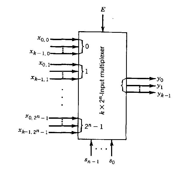
Fig. 1.40 - Kx2-input (vector) multiplexers.