

Invitation to a Contemporary Physics (2004)
.pdf5.4. Quantum Devices |
165 |
is made wider, thereby accommodating successive higher-order wave guide modes (Fig. 5.6). Recent experiments indicate, however, a more complex situation that involves the electron spin in some decisive way, leading to an additional conductance structure at 0.7G0 (Problem 5.5).
5.4.3 Quantum Dots
Quantum dots, the ultimate in confinement, are solid-state structures that contain mobile electrons in a ‘box,’ or a very small conducting region surrounded on all sides either by insulating materials or by electric fields which produce the potential needed for confining the electrons. If the confinement is robust enough and the size of the box small enough, quantum e ects can be observed macroscopically. Like natural atoms, quantum dots contain a countable number of electrons (ranging from a few to a few hundred thousands) and display a spectrum of sharp energy levels, leading to the frequent reference to them as ‘artificial atoms.’ The growing interest in them is of a fundamental nature as well as strongly driven by potential applications where their small size and discrete energy spectrum would be beneficial.
However, the two types of electronic systems also di er on several significant points. First, while in real atoms confinement of electrons is caused by the electrostatic force of the nucleus, in artificial atoms it is accomplished by material boundaries or electrodes whose shape and strength control the shape, size and symmetry of the confining potential. Quantum dots have been created and studied, with or without symmetry and in various geometries, including rods, pancakes and spheres. Secondly, the relevant length and energy scales are not the same, with the typical size and Fermi energy in naturally occurring metal clusters being around 0.5 nm and 5 eV, whereas the corresponding values in semiconductor nanostructures are 50 nm and 10 meV, respectively. It means that both the thermal motion and the electron–electron interaction play a relatively more important role in the much larger artificial atom than in the smaller real atom (Problems 5.6 and 5.7).
One possible way to construct a quantum box is to surround a small region of a two-dimensional electron system with lateral walls. To implement this idea, a crystal wafer is grown layer by layer, starting from the bottom (Fig. 5.7). One begins with a heavily doped crystal of GaAs, which serves as a metal gate, over which one grows by MBE a layer of AlGaAs, thin enough to let electrons leak through it. Next, one grows a layer of pure GaAs, which is where the electrons will accumulate and form a 2DES when a positive voltage VG is applied to the gate. Finally, a pair of tiny longish specially shaped metal electrodes, which look like two gaping jaws baring their teeth, are deposited on top of the crystal wafer. In addition, two contacts (called source and drain) are placed at the ends of the electrodes to allow electrons to enter or leave the system. The metal plates are negatively biased and so repel the electrons in the 2DES lying directly underneath, thereby erecting potential barriers that separate a shallow pool of charges within

166 |
Exploring Nanostructures |
Au electrodes |
Drain |
|
Source
Ga As e
Al Ga As
Ga As (doped)
(a)Back Gate
/h) 2
(eConductance
(b)
10–1
10–2
10–3
10–4
Gate voltage
Figure 5.7: Zero-dimensional confined system. (a) Schematic of a quantum dot. (b) Conductance of a quantum dot a as function of the gate voltage, showing sharp peaks at equal intervals (adapted from Marc Kastner, 1993).
the perimeter formed by the electrodes and the split gates from all the electrons left outside. This quasi-zero-dimensional pool of electron gas is our quantum dot, also called Coulomb island. For a su ciently large negative bias voltage, each constriction (or gap in the potential barrier under a pair of opposing metal teeth) is completely closed o , and electrons must tunnel through it. But when the voltage is made less negative, the constriction begins to open up, letting a current pass freely through.
To probe this little box, you may imagine changing its charge content ever so slightly. What work does it take, you’d ask, to add the smallest possible speck of charge? Assuming there is no charge in the box and no applied voltage to begin with, you need an energy Q2/2C to add a charge Q to a dot with total capacitance C (which is proportional to the island’s diameter and of the order of 10−16 farad). Since you cannot add less than an electron, a transfer of charge onto the island costs at least e2/2C in energy: charge quantization requires an electron to have an energy e2/2C above the Fermi level in the contact in order to hop onto the island, and a hole to have an energy lower than the Fermi level by the same amount in order to cross the tunnel. So you see, in the absence of an applied voltage, no current can flow through the system as long as the thermal energy stays below the minimum charging energy e2/C, a phenomenon known as the Coulomb blockade.
However, when we apply a voltage VG at the bottom plate, the attractive interaction between the negative charge Q and the positively charged gate must be added to the repulsive interaction among the bits of charge on the dot to give the total electrostatic (charging) energy:
Q2
E = QVG + 2C .

5.4. Quantum Devices |
167 |
This equation tells us that, as a function of Q, the energy E has a minimum at induced charge Q0 = −CVG or, equivalently, at gate voltage VG = −Q0/C. When Q0 = −Ne, or VG = Ne/C, an integral number N of electrons minimizes E, but the Coulomb interaction still demands an amount of energy e2/2C to either add or remove one electron. Given the control we have over the applied voltage, we may wonder if, near this optimum number N, we can find a value of VG for which it would cost us less (and hopefully nothing) to add or remove a charge quantum. As VG varies continuously, it may be written in the form VG = (N + δ)e/C, where δ is a number between 0 and 1. We will write the energy as E(N) to emphasize its dependence on the charge number N = −Q/e, and readily show that the states with N and N + 1 electrons di er in energy by E(N + 1) − E(N) = (1 − 2δ)e2/2C, a quantity independent of N. We see that as δ is varied from 0 to 1, this energy di erence goes from being positive to being negative in passing by zero at δ = 0.5. In other words, if the dot finds it energetically more favorable to have N electrons at a voltage below VG = (N + 0.5)e/C, then for higher voltages it would prefer to have one additional electron. However, when the voltage is set precisely at that value, the two configurations have equal energies, and the charge fluctuates between
−Ne and −(N + 1)e even at zero temperature. This fluctuation occurs when an electron tunnels onto the dot from the left lead, and later another tunnels o the dot to the right lead (Problem 5.8).
When a very small, fixed voltage is applied between the source and drain, just large enough to coax the electrons to move along, we can measure the tunneling current through the quantum dot as the gate voltage VG is varied. Sharp current peaks appear periodically at gate voltage VG = (N + 0.5)e/C and every time the voltage increases by steps of e/C, which is the amount necessary to add one more electron to the confined pool of electrons. So, increasing the gate voltage of an artificial atom is equivalent to moving through the periodic table of real atoms. While a range of voltages produces no current at all, a sharp spectacular current spike appears when the voltage reaches the next critical value, and we know then that another electron has just hopped into the pool. Whereas thousands of charge carriers must flow (and produce a large amount of heat) each time a traditional semiconductor transistor flips, it su ces a single electron to turn a quantum dot on and o again. That is why some people consider, justifiably, a quantum dot a single-electron transistor (SET).
This unique transport property of the single-electron transistor is the basis of operation for several devices, such as electrometers and electron turnstiles, which require extreme charge sensitivity. Even more promising in terms of new physics and new applications are artificial molecules, consisting of two or more closely spaced quantum dots, and artificial solids, made of large arrays of linked quantum dots. The exciting feature here is that the researchers can control the strengths of interactions between neighboring artificial atoms by varying at will the voltages on electrodes, and thereby learn to engineer desired properties into artificial matter.

168 |
Exploring Nanostructures |
5.4.4Summary
Starting from the basic concepts of the quantum well, quantum wire and quantum dot, researchers have made use of the control they have over the fabrication process — the parameters of confinement, the choice of the primary materials, and the composition and architecture of the structures — to design novel or improved devices. The quantum-cascade laser and the single-electron transistor are good examples of the photonic or electronic devices that exploit judiciously the unique electronic and transport properties of systems having lesser dimensions.
5.5 The Genius of Carbon
Nature endows carbon with a wonderful versatility: by exploiting its bonding to the full, it can build structures in all dimensionalities. Diamond is a three-dimensional lattice, graphite is a stack of two-dimensional layers, and other carbon structures are found so small that they may be considered oneor zero-dimensional.
5.5.1 Carbon Fullerenes
The extraordinary all-carbon molecule C60 has become one of the best known nanostructures. An interesting story behind its discovery, a pretty name and an alluring shape also help.
The experiments that led to its discovery in 1985 were aimed at simulating in laboratory the conditions under which carbon atoms cluster in the atmosphere of a carbon-rich red giant star and, specifically, at exploring the possibility that long carbon chain molecules could form when carbon nucleates in the presence of hydrogen and nitrogen. In these experiments, an intense pulsed laser beam, focused on a rotating graphite disk, vaporized the material, and the resulting carbon vapor was entrained in a powerful stream of helium, which, being a chemically inert gas, cooled the vapor so that it could condense into small clusters. As the carrier gas expanded through a nozzle into a vacuum, it produced a jet of cold clusters whose masses could be measured by a mass spectrometer. Reactive gases such as hydrogen or nitrogen could also be added to the carrier gas, and the products of the reactions of these gases with the carbon clusters could be similarly analyzed. The experiments showed that species such as HC7N and HC9N could indeed be produced, but, unexpectedly, a host of even-numbered clusters with 38–120 carbon atoms were also generated in a roughly Gaussian mass distribution strongly dominated by C60 (Fig. 5.8). The leaders of the experiments, Robert Curl, Harold Kroto and Richard Smalley, realized that the unusually high stability of C60 could be explained by a molecular structure having the perfect symmetry of a soccer ball, and called the molecule buckminsterfullerene, or buckyball for short, because its shape was reminiscent of the geodesic domes popularized by architect R. Buckminster Fuller.

5.5. The Genius of Carbon |
169 |
Relative Abondance
C60
C70
Atomic Weight
Light Absorption
Wavelength
Figure 5.8: Crucial graphs in the discovery of C60. In 1985 the cluster-beam generator showed the presence of many even-numbered carbon clusters, especially C60. In 1990 Kr¨atschmer and Hu man showed that this humped ultraviolet absorption spectrum revealed the presence of C60.
Although they did not have direct evidence to support their conjecture, subsequent experiments in spectroscopy and crystallography have proven them right, which earned them the 1996 Nobel Prize in Chemistry.
The proposed structure for C60 looks like a hollow truncated icosahedron obtained from an icosahedron by snipping o each of its twelve vertices. As a result, each vertex of the Platonic polyhedron is replaced by a pentagon, and each triangular face converted into a hexagon (Fig. 5.9). With the sixty atoms evenly distributed among its vertices, the truncated icosahedral structure has exceptional strength and stability (Problem 5.9).
The carbon atom has four valence electrons occupying an outer shell, which is only half full. By combining with other elements which have similar, incomplete shell structures, and by sharing with them one or more pairs of valence electrons (thus creating single, double or triple bonds), it can form a stable molecule. It
(a) |
(b) |
Figure 5.9: Structure of C60. When the vertices of a regular icosahedron are snipped o , one obtains a truncated icosahedron, which gives the framework for C60. The carbon atoms are located at the vertices, and the double bonds at the two-hexagon fusions.

170 |
Exploring Nanostructures |
can also bond with other carbon atoms in di erent ways to create structures with entirely di erent properties. When the four valence electrons of a carbon atom are shared equally with four other carbon atoms sitting at the vertices of a tetrahedron whose center is occupied by the given atom, we have, assuming an infinite lattice, isotropically strong diamond. When only three are shared between neighbors, with the fourth moving freely among atoms, we have graphite, a layered material possessing highly anisotropic properties. Strength, elastic modulus, electric conductivity, and thermal conductivity are much higher within the covalently bonded planes than across them. In bulk solid phase, graphite is thermodynamically stable up to very high temperatures under normal pressure. But in a finite chunk, atoms at the surfaces, having no carbon neighbors, must tie up their unsatisfied (dangling) bonds with hydrogen in the air. Similarly, in a synthesis process where there are fewer than a few hundred carbon atoms available at any given time, the growing structures will seek energetically favorable, finite configurations — linear chains, rings or closed shells — that keep dangling bonds to a minimum.
Once monocyclic rings are formed, they can grow by adding further atoms or small chains, and fold into polycyclic networks, which resemble pieces of hexagonal graphite lattice or fragments of chicken wire. The general physical tendency to reach the lowest-energy level induces the planar sheets to eliminate the unsatisfied valences of the edge atoms by curling up. To curl up, or to produce a convex curved structure, the sheets rearrange their bonding so that five-membered rings are formed, enabling the dangling bonds of some of the edge atoms to tie up into good carbon–carbon bonds. As the process continues, there is a high probability that the graphitic sheets curl until the opposing edges meet to create closed cage-like structures of nanometric dimensions.
A closed cage-like molecule that contains only hexagonal and pentagonal faces is called a fullerene. This definition leaves out heptagons and octagons, which are responsible for the concave parts and treated as defects. Like any simple polyhedron, a fullerene satisfies Euler’s theorem, which relates the numbers of vertices (carbon atoms) v, edges (covalent bonds) e, and faces f:
v − e + f = 2 .
Let p be the number of pentagons, and h = f − p the number of hexagons. As each vertex radiates into three edges and each edge joins two vertices, the doubled number of edges equals the tripled number of vertices, 2e = 3v, which is also 5p + 6h since each edge belongs to two adjacent faces. A simple calculation yields p = 12, meaning that exactly 12 pentagons are required to provide the curvature needed to close a hexagonal lattice into a defect-free fullerene. The addition of each hexagonal face increases the total number of vertices and hence the number of atoms by two, so the total number of carbon atoms in a fullerene must be even, according to v = 2(h+10), which is consistent with the observed mass spectra. The smallest fullerene, C20, corresponds to h = 0, but no closed cage can be formed with h = 1, and C22 has

5.5. The Genius of Carbon |
171 |
never been observed. Otherwise, any number of hexagons is allowed, and one could imagine an elongated fullerene with exactly 12 pentagons and millions of hexagons. However, not all such constructions are stable. For example, two adjacent pentagons would be energetically unfavorable compared with isolated pentagons, because they would give higher local curvature and hence more strain to the structure. That is why unsaturated organic molecules with contiguous pentagonal rings are rarely found; a chemically stable molecule cannot have adjacent pentagonal rings. The molecules C60 and C70 are the two lowest-mass carbon fullerenes that satisfy both Euler’s 12-pentagonal closure principle and the isolated-pentagon rule and, for this reason, appear prominently in the observed mass distributions of carbon clusters (Problems 5.10 and 5.11).
C60 is now produced in quantities large enough to make solids (fullerite) of weakly bound molecules. Pure C60 solid is an insulator. When it is doped with alkali atoms, these impurities contribute electrons to the lowest empty band of the fullerite, and the compound thus formed becomes insulating or conducting (i.e., metallic), depending on the degree of electronic occupation. At low temperatures, not only some of these compounds (such as A3C60, where A = K, Rb, Cs), but also alloys C60-alkaline-earth (e.g., Ba6C60, Sr6C60) and C60-rare-earth (e.g., Yb2.75C60) are superconducting, with a transition temperature Tc that is surpassed only by the cuprates (Chapter 3). Thus, Tc is 33 K for RbCs2C60 and 40 K for Cs3C60 under pressure. The trend seems to suggest that even higher Tc could be obtained by incorporating larger cations. Other workers, taking a di erent approach, showed that fullerite doped with holes, rather than electrons, became superconducting at 52 K.
Within days of the discovery of C60, Smalley and his collaborators found that metal atoms could be trapped inside fullerenes by impregnating graphite with the desired metal before exposing it to laser vaporization. A carbon fullerene Cn encaging a metal atom M is called an endohedral metallofullerene and written M@Cn or, alternatively, fullerene-incar-metal and written iMCn. All such complexes are of the ship-in-a-bottle type, and many have been synthesized, including radioactive species, which raises the prospect of their applications in materials, biological and medical science. In 1992 Daniel Ugarte announced that under high-energy electron irradiation, nested fullerenes could be generated. These ‘graphitic onions’ are of considerable size, with diameters up to 47 nm, and contain thousands, even millions, of carbon atoms in spherical shells separated by spacings of 0.335 nm, just as layers in graphite. As nested structures, they are a special form of multiwalled nanotubes.
5.5.2 Carbon Nanotubes
A carbon nanotube is a single molecule of many carbon atoms arranged in a hexagonal network that curls into a long, slender tubule capped at each end, and is comparable in all respects to a very elongated fullerene. It exists in singles, known

172 |
Exploring Nanostructures |
as single-wall nanotubes, or in nested multiples, called multiwalled nanotubes. The latter — the first of the two to be discovered, by Sumio Iijima in 1991, in samples created by arc discharges between carbon electrodes immersed in a noble gas — consist of several concentric cylindrical shells of graphitic sheets co-axially arranged around a central hollow with a constant separation between the layers. They have diameters ranging from 2 to 25 nm and lengths up to many micrometers. Single-wall nanotubes are cylinders made of single sheets of graphene (one-atom thick layers of graphite), with diameters distributed in a narrow range (1–2 nm). When produced in the vapor phase, single-wall nanotubes self-assemble into larger bundles (ropes) that consist of tens of nanotubes.
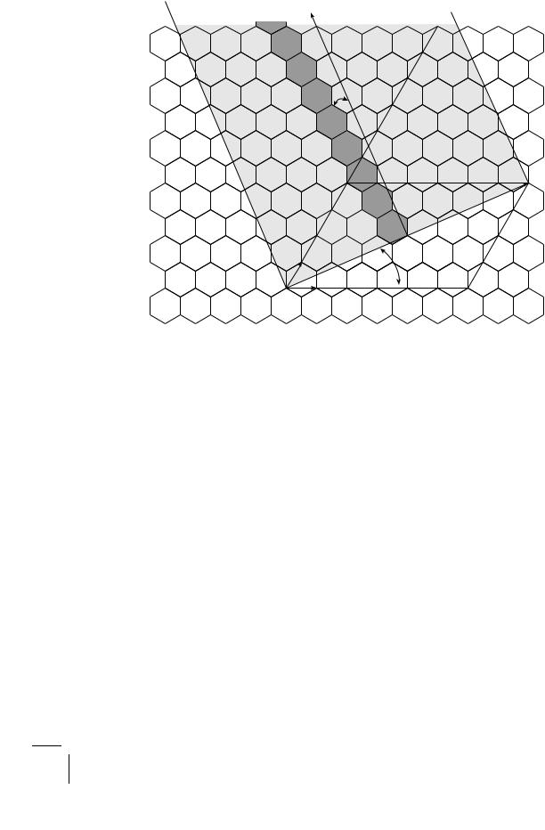
Suppose you want to build an ideal single-wall carbon nanotube. First, take a rectangular sheet of graphene (chicken wire), then roll it up into a cylinder such that the dangling bonds (open wire fragments) at opposing edges match perfectly to form a seamless tube, and, finally, close the open ends of the tube with the hemispheric domes obtained from a fullerene by cutting it evenly in half. Depending on the width of your rectangle, you may roll in one of several directions relative to some fixed row of bonds, so that on the curved surface of the tube the hexagonal arrays of
(0,5) |
B |
(5,5) |
arm chair
a2
A
(0,0) |
a1 |
(5,0) |
|
zigzag |
A |
B |
(0,0) |
(9,0) |
Figure 5.10: Construction of an armchair nanotube (5, 5) and a zigzag nanotube (9, 0). Colored hexagons indicate the direction of the tube axis. The rolling is along the vector AB.
5.5. The Genius of Carbon |
173 |
|
|
|
|
|
|
|
|
|
|
|
|
|
|
|
|
|
|
|
|
|
|
|
|
|
|
|
|
|
|
|
|
|
|
|
|
|
|
|
|
|
|
|
|
|
|
|
|
|
|
|
|
|
|
|
|
|
|
|
|
|
|
|
|
|
|
|
|
|
|
|
|
|
|
|
|
|
|
|
|
|
|
|
|
|
|
|
|
|
|
|
|
|
|
|
|
|
|
|
|
|
|
|
|
|
|
|
Figure 5.11: Construction of a chiral nanotube (6, 4). Also indicated is the winding angle φ defined with respect to the tube axis.
carbon atoms may wind around in a helical fashion with a constant winding angle with respect to the tube axis. To give a more precise description, let us define a vector joining two sites, A and B, on the lattice by a pair of integers n and m, which record the numbers of steps starting from point A and going along two reference axes. This vector defines the wrapping into a tube of circumference AB if after folding along its direction, points A = (0, 0) and B = (n, m) coincide, so that (n, m) contain all information on the structure (diameter and winding angle) of the tube, and hence may serve to characterize it. Thus, the indices (n, 0) designate zigzag nanotubes, and (n, n) armchair nanotubes (Fig. 5.10), whereas all other possibilities are termed chiral or helical (Fig. 5.11). Because of their simple and well-defined structure, single-wall nanotubes serve as models for theoretical calculations and key experiments (Problem 5.12).
What makes the carbon nanotubes fascinating is their wide-ranging superior properties, which result from a unique combination of dimension, topology and structure. For example, their light weight (1 g/cm3) results from a hollow cagelike architecture, their relatively large surface area (10 m2/g) is due to nanometric dimensions, and they owe their unusual capillary behavior to the smooth, straight,

174 |
Exploring Nanostructures |
one-dimensional channel in their center. All these properties make nanotubes useful as catalysts, components of novel materials, atomic-sized storage systems and templates for fabrication of nanostructures.
Even more remarkable are their mechanical properties, which they inherit from their graphitic frame and improve with their distinctive geometry. Carbon fibers, which are long strands of graphene, have been used for decades to strengthen a variety of substances, and nanotubes are predicted to be by far the strongest fibers that can be made. A combination of great strength and light weight make them ideal as materials for transport and construction. The Young’s modulus of a nanotube, which is a measure of its elastic strength, or its degree of resistance to deformation, can be obtained by measuring the thermal vibrations of the free end of the tube clamped at the other end. The result found is consistent with the value for a graphene sheet, which reaches 1 terapascal, or five times the value for steel. But, because of their hollow structure and closed topology, carbon nanotubes respond to extreme strains in a way quite di erent from other graphitic structures. Unlike carbon fibers, they can be bent, twisted or compressed without breaking, and will regain their original shape when the applied stress is released. The reversibility of deformations, such as buckling, has been recorded in electron microscope images, and indicates that nanotubes are highly elastic. Such superior mechanical properties make them promising in reinforcement applications and for use as tips or tools in proximity probe microscopy.
Apart from their special structural attributes, nanotubes possess equally intriguing electronic properties. In graphite, there is no band gap between the empty and full states, but there are also very few free electrons (one per 104 atoms, compared to one per atom in copper) capable of carrying charges along the graphene sheets. Graphite therefore is not quite a conductor: it is a semimetal. In nanotubes, we have the same electronic structure but an entirely di erent situation.
The di erences stem from the fact that the free electrons in a nanotube are confined to the one-dimensional geometry of a thin cylinder. The electrons can propagate freely in only one direction, along the tube, rather than in the two directions that were available in the graphene plane, being constrained in the transverse direction to move around the tube. The periodic boundary condition imposed on the wave function by this confinement means that only a whole number of wavelengths can fit around the tube, and so the electron wave vector around the circumference is quantized. Since this quantization depends on the circumference and winding angle, it follows that the electronic states and energies must depend on the indices n and m of the nanotube.
Calculations predict, and experiments concur, that armchair tubes have valence and conduction bands crossing at the Fermi level and are, therefore, metallic. Among the other (chiral and zigzag) tubes, one third (those for which n − m = 3l, where l is an integer) are metallic, and two thirds (for which n − m =l3) semiconducting (Problem 5.13).