

AD822
APPLICATIONS
Single-Supply Voltage-to-Frequency Converter
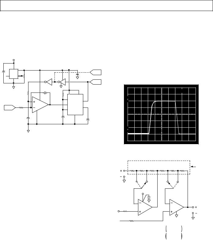
The circuit shown in Figure 7 uses the AD822 to drive a low power timer that produces a stable pulse of width t1. The positive going output pulse is integrated by R1–C1 and used as one input to the AD822 that is connected as a differential integrator. The other input (nonloading) is the unknown voltage, VIN. The AD822 output drives the timer trigger input, closing the overall feedback loop.
+10V |
|
|
U4 |
|
|
|
|
|
|
|
|
|
|
|
|
|
|
C5 |
|
REF02 |
|
|
|
|
|
|
0.1 F |
2 |
6 VREF = 5V |
|
|
|
|
|
|
|
|
5 |
|
CMOS |
|
|
|
OUT2 |
3 |
|
RSCALE** |
74HCO4 |
|
|
|
C3 |
|
|
4 |
|
10k |
4 U3B |
|
U3A |
|
0.1 F |
|
|
|
3 |
2 |
1 |
OUT1 |
||
|
|
|
|
|
|
|
|
|
|
|
|
|
|
|
|
U2 |
|
|
|
|
|
0.01 F, 2% |
|
CMOS 555 |
||
|
|
|
R2 |
|
|
8 |
||
|
|
|
|
|
R3* |
4 |
||
|
499k 1% |
|
|
|||||
|
C1 |
|
R |
V+ |
||||
|
|
|
U1 |
|
116k |
|||
|
|
|
|
|
|
6 |
3 |
|
|
|
|
|
|
|
|
THR |
|
|
|
|
1/2 |
|
|
2 |
OUT |
|
VIN |
|
R1 |
AD822B |
|
|
TR |
5 |
|
499k 1% |
|
|
|
7 |
CV |
|||
|
|
|
|
DIS |
|
|||
|
|
|
C2 |
|
|
|
GND |
|
|
|
|
|
|
|
1 |
C4 |
|
|
0.01 F, 2% |
|
|
|
||||
|
|
|
|
|
||||
|
|
|
|
|
|
|
|
0.01 F |
0V TO 2.5V |
NOTES |
|
FULL SCALE |
||
|
fOUT = VIN/(VREF t1), t1 = 1.1 R3 C6
= 25kHz FS AS SHOWN
*= 1% METAL FILM, <50ppm/ C TC
**= 10% 20T FILM, <100ppm/ C TC
t1 = 33 s FOR fOUT = 20kHz @ VIN = 2.0V
Figure 7. Single-Supply Voltage-to-Frequency Converter
Typical AD822 bias currents of 2 pA allow megohm-range source impedances with negligible dc errors. Linearity errors on the order of 0.01% full scale can be achieved with this circuit. This performance is obtained with a 5 V single supply that delivers less than 1 mA to the entire circuit.
Single-Supply Programmable Gain Instrumentation Amplifier
The AD822 can be configured as a single-supply instrumentation amplifier that is able to operate from single supplies down to 3 V or dual supplies up to ±15 V. Using only one AD822 rather than three separate op amps, this circuit is cost and power efficient. AD822 FET inputs’ 2 pA bias currents minimize offset errors caused by high unbalanced source impedances.
An array of precision thin-film resistors sets the in amp gain to be either 10 or 100. These resistors are laser trimmed to ratio match to 0.01% and have a maximum differential TC of 5 ppm/∞C.
Table I. In Amp Performance
Parameters |
|
VS = 3 V, 0 V |
VS = 65 V |
||||
CMRR 74 dB |
|
80 dB |
|
|
|||
Common-Mode |
|
|
|
|
|
|
|
Voltage Range |
|
–0.2 V to +2 V |
–5.2 V to +4 V |
||||
3 dB BW, G = 10 |
|
180 kHz |
180 kHz |
||||
|
G = 100 |
|
18 kHz |
18 kHz |
|||
tSETTLING |
|
2 μs |
|
|
|||
2 V Step (VS = 0 V, 3 V) |
5 μs |
||||||
5 V (VS = ±5 V) |
|
270 nV/ Hz |
|||||
Noise @ f = 1 kHz, G = 10 |
270 nV/ Hz |
||||||
|
|
G = 100 |
2.2 μV/ Hz |
2.2 μV/ Hz |
|||
ISUPPLY (Total) |
1.10 mA |
1.15 mA |
|
|
|||
|
|
|
|
|
|
|
|
|
|
|
|
|
|
|
|
|
|
|
|
5µs |
|
|
|
100 . . . . . . . . . . . . . . . . . . . . . . . . . . . . . . . . . . . . . . . . |
|
||||||
90 |
|
|
|
|
|
|
|
. |
|
|
|
|
|
|
|
10 0% . . . . . . . . . . . . . . . . . . . . . . . . . . . . . . . . . . . . . . . .
1V
Figure 8a. Pulse Response of In Amp to a 500 mV p-p Input Signal; VS = 5 V, 0 V; Gain = 10
|
R1 |
R2 |
R3 |
R4 |
R5 |
R6 |
OHMTEK |
|
90k |
9k |
1k |
1k |
9k |
90k |
PART # 1043 |
VREF |
|
|
|
|
|
|
|
|
G = 10 |
G = 100 |
G = 100 |
|
G = 10 |
|
|
|
|
+VS |
0.1 F |
|
|
|
|
|
|
|
|
|
|
|
|
|
2 |
|
|
6 |
|
7 |
|
RP |
|
1/2 |
1 |
|
1/2 |
|
|
|
|
|
|
||||
1k |
3 |
AD822 |
|
5 |
AD822 |
VOUT |
|
VIN1 |
|
|
|
|
|
4 |
|
RP 1k
VIN2 
R6
(G = 10) VOUT = (VIN1 – VIN2) 1+ –––––––– +VREF R4 + R5
R5 + R6
(G = 100) VOUT = (VIN1 – VIN2) 1+ –––––––– +VREF R4
Figure 8b. A Single-Supply Programmable
Instrumentation Amplifier
REV. E |
–15– |
AD822
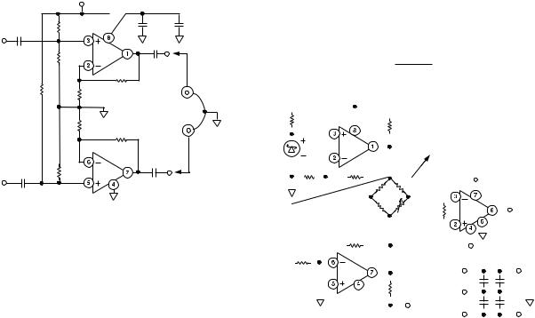
3 V, Single-Supply Stereo Headphone Driver
The AD822 exhibits good current drive and THD + N performance, even at 3 V single supplies. At 1 kHz, total harmonic distortion plus noise (THD + N) equals –62 dB (0.079%) for a 300 mV p-p output signal. This is comparable to other singlesupply op amps that consume more power and cannot run on 3 V power supplies.
|
|
3V |
|
|
1 F |
|
|
+ |
|
95.3k |
0.1 F |
0.1 F |
||
MYLAR |
||||
|
|
|
||
CHANNEL 1 |
|
1/2 |
|
|
|
|
|
||
|
47.5k |
AD822 |
|
|
|
|
500 F |
|
|
|
|
4.99k |
|
|
95.3k |
10k |
L |
||
|
|
|||
|
|
HEADPHONES |
||
|
|
32 IMPEDANCE |
||
|
10k |
|
||
|
|
4.99k |
R |
|
1 F |
47.5k |
1/2 |
|
|
MYLAR |
AD822 |
|
||
CHANNEL 2 |
|
500 F |
|
|
Figure 9. 3 V Single-Supply Stereo Headphone Driver
In Figure 9, each channel’s input signal is coupled via a 1 μF Mylar capacitor. Resistor dividers set the dc voltage at the noninverting inputs so that the output voltage is midway between the power supplies (1.5 V). The gain is 1.5. Each half of the AD822 can then be used to drive a headphone channel. A 5 Hz high-pass filter is realized by the 500 μF capacitors and the headphones that can be modeled as 32 Ω load resistors to ground. This ensures that all signals in the audio frequency range (20 Hz to 20 kHz) are delivered to the headphones.
Low Dropout Bipolar Bridge Driver
The AD822 can be used for driving a 350 Ω Wheatstone bridge. Figure 10 shows one half of the AD822 being used to buffer the AD589—a 1.235 V low power reference. The output of 4.5 V can be used to drive an A/D converter front end. The other half of the AD822 is configured as a unity gain inverter and generates the other bridge input of –4.5 V. Resistors R1 and R2 provide
a constant current for bridge excitation. The AD620 low power instrumentation amplifier is used to condition the differential output voltage of the bridge. The gain of the AD620 is programmed using an external resistor RG and determined by:
|
G = 49.4kΩ + 1 |
|
||
|
|
RG |
|
|
|
+Vs |
|
|
|
49.9k |
|
R1 |
|
|
+1.235V |
|
|
|
|
|
20 |
|
|
|
AD589 |
1/2 |
TO A/D CONVERTER |
||
AD822 |
REFERENCE INPUT |
|||
|
25.4k 1% |
|
|
+VS |
10k 1% |
350 |
350 |
|
|
|
|
|
||
|
|
|
|
|
|
350 |
350 |
RG |
AD620 |
|
10k 1% |
|
VREF |
|
|
||
|
|
|
|
|
|||
|
|
|
–VS |
|
|
|
|
10k 1% |
1/2 |
–4.5V |
+Vs |
|
|
+5V |
|
AD822 |
+ |
+ |
|||||
|
R2 |
0.1 F |
1 F |
||||
|
|
|
|
|
|
||
|
|
20 |
GND |
+ |
+ |
|
|
|
|
–Vs |
0.1 F |
1 F |
|||
|
|
|
–Vs |
|
|
–5V |
|
Figure 10. Low Dropout Bipolar Bridge Driver
–16– |
REV. E |