


AD822
ABSOLUTE MAXIMUM RATINGS1
Supply Voltage . . . . . . . . . . . . . . . . . . . . . . . . . . . . . . . . ±18 V Internal Power Dissipation2
Plastic DIP (N) . . . . . . . . . . . . . . . Observe Derating Curves SOIC (R) . . . . . . . . . . . . . . . . . . . Observe Derating Curves
Input Voltage . . . . . . . . . . . . . . (+VS + 0.2 V) to –(20 V + VS) Output Short Circuit Duration . . . . . . . . . . . . . . . . Indefinite
Differential Input Voltage . . . . . . . . . . . . . . . . . . . . . . . ±30 V Storage Temperature Range (N) . . . . . . . . . –65∞C to +125∞C Storage Temperature Range (R, RM) . . . . . –65∞C to +150∞C Operating Temperature Range
AD822A/AD822B . . . . . . . . . . . . . . . . . . . –40∞C to +85∞C Lead Temperature Range (Soldering, 60 sec) . . . . . . . . 260∞C
NOTES
1Stresses above those listed under Absolute Maximum Ratings may cause permanent damage to the device. This is a stress rating only; functional operation of the device at these or any other conditions above those indicated in the operational section of this specification is not implied. Exposure to absolute maximum rating conditions for extended periods may affect device reliability.
28-Lead Plastic DIP Package: JA = 90∞C/W 8-Lead SOIC Package: JA = 160∞C/W 8-Lead MSOP Package: JA = 190∞C/W
MAXIMUM POWER DISSIPATION
The maximum power that can be safely dissipated by the AD822 is limited by the associated rise in junction temperature. For plastic packages, the maximum safe junction temperature is 145∞C. If these maximums are exceeded momentarily, proper circuit operation will be restored as soon as the die temperature is reduced. Leaving the device in the “overheated” condition for an extended period can result in device burnout. To ensure proper operation, it is important to observe the derating curves shown in TPC 24.
While the AD822 is internally short circuit protected, this may not be sufficient to guarantee that the maximum junction temperature is not exceeded under all conditions. With power supplies
±12 V (or less) at an ambient temperature of 25∞C or less, if the output node is shorted to a supply rail, then the amplifier will not be destroyed, even if this condition persists for an extended period.
ORDERING GUIDE
Model* |
Temperature Range |
Package Description |
Package Option |
Branding Information |
|
|
|
|
|
AD822AN |
–40∞C to +85∞C |
8-Lead PDIP |
N-8 |
|
AD822AR |
–40∞C to +85∞C |
8-Lead SOIC |
R-8 |
|
AD822ARM |
–40∞C to +85∞C |
8-Lead MSOP |
RM-8 |
B4A |
AD822BR |
–40∞C to +85∞C |
8-Lead SOIC |
R-8 |
|
*SPICE model is available at www.analog.com.
CAUTION
ESD (electrostatic discharge) sensitive device. Electrostatic charges as high as 4000 V readily accumulate on the human body and test equipment and can discharge without detection. Although the AD822 features proprietary ESD protection circuitry, permanent damage may occur on devices subjected to high energy electrostatic discharges. Therefore, proper ESD precautions are recommended to avoid performance degradation or loss of functionality.
–6– |
REV. E |
Typical Performance Characteristics– AD822
|
70 |
|
|
|
|
|
|
|
|
|
|
|
60 |
|
|
|
|
|
|
|
VS = 0V, 5V |
|
|
|
|
|
|
|
|
|
|
|
|
|
|
UNITS |
50 |
|
|
|
|
|
|
|
|
|
|
40 |
|
|
|
|
|
|
|
|
|
|
|
OF |
|
|
|
|
|
|
|
|
|
|
|
|
|
|
|
|
|
|
|
|
|
|
|
NUMBER |
30 |
|
|
|
|
|
|
|
|
|
|
|
|
|
|
|
|
|
|
|
|
|
|
|
20 |
|
|
|
|
|
|
|
|
|
|
|
10 |
|
|
|
|
|
|
|
|
|
|
|
0 |
|
|
|
|
|
|
|
|
|
|
|
–0.5 |
–0.4 |
–0.3 |
–0.2 |
–0.1 |
0 |
0.1 |
0.2 |
0.3 |
0.4 |
0.5 |
|
|
|
|
OFFSET VOLTAGE – mV |
|
|
|
||||
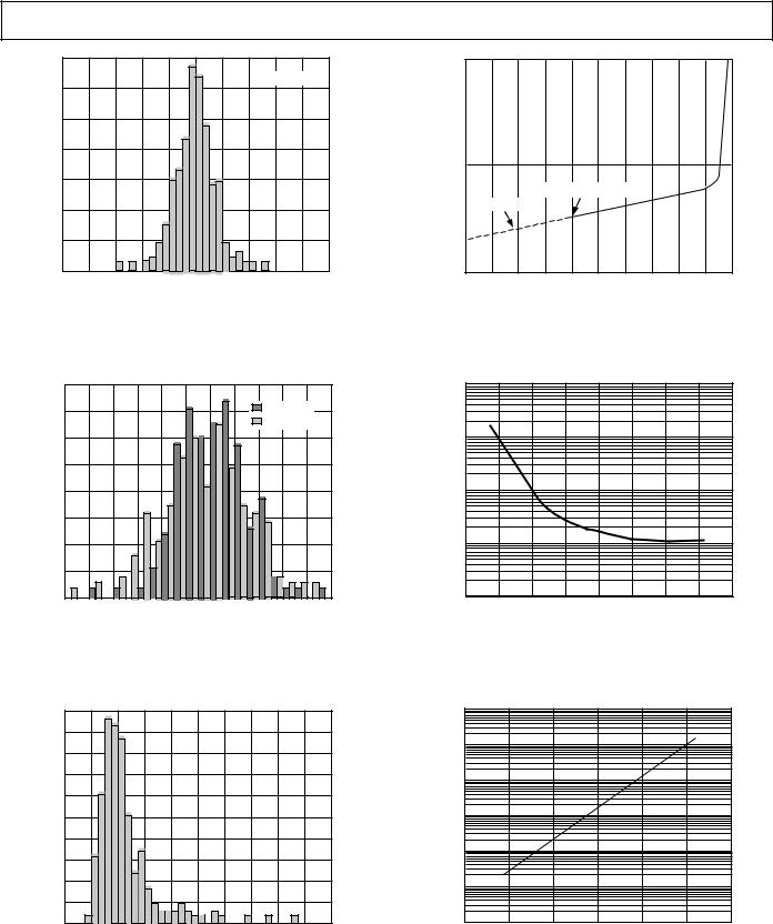
TPC 1. Typical Distribution of Offset Voltage (390 Units)
|
16 |
|
|
|
|
|
|
|
|
|
|
|
|
14 |
|
|
|
|
|
|
|
|
VS = 5V |
|
|
|
|
|
|
|
|
|
|
|
|
VS = 15V |
|
|
|
12 |
|
|
|
|
|
|
|
|
|
|
|
|
10 |
|
|
|
|
|
|
|
|
|
|
|
BIN |
8 |
|
|
|
|
|
|
|
|
|
|
|
% IN |
|
|
|
|
|
|
|
|
|
|
|
|
6 |
|
|
|
|
|
|
|
|
|
|
|
|
|
|
|
|
|
|
|
|
|
|
|
|
|
|
4 |
|
|
|
|
|
|
|
|
|
|
|
|
2 |
|
|
|
|
|
|
|
|
|
|
|
|
0 |
|
|
|
|
|
|
|
|
|
|
|
|
–12 |
–10 |
–8 |
–6 |
–4 |
–2 |
0 |
2 |
4 |
6 |
8 |
10 |
|
|
|
|
OFFSET VOLTAGE DRIFT – V/ C |
|
|
||||||
TPC 2. Typical Distribution of Offset Voltage Drift
(100 Units)
|
50 |
|
|
|
|
|
|
|
|
|
|
|
45 |
|
|
|
|
|
|
|
|
|
|
|
40 |
|
|
|
|
|
|
|
|
|
|
|
35 |
|
|
|
|
|
|
|
|
|
|
UNITS |
30 |
|
|
|
|
|
|
|
|
|
|
25 |
|
|
|
|
|
|
|
|
|
|
|
OF |
|
|
|
|
|
|
|
|
|
|
|
|
|
|
|
|
|
|
|
|
|
|
|
NUMBER |
20 |
|
|
|
|
|
|
|
|
|
|
15 |
|
|
|
|
|
|
|
|
|
|
|
|
|
|
|
|
|
|
|
|
|
|
|
|
10 |
|
|
|
|
|
|
|
|
|
|
|
5 |
|
|
|
|
|
|
|
|
|
|
|
0 |
|
|
|
|
|
|
|
|
|
|
|
0 |
1 |
2 |
3 |
4 |
5 |
6 |
7 |
8 |
9 |
10 |
|
|
|
|
INPUT BIAS CURRENT – pA |
|
|
|
||||
TPC 3. Typical Distribution of Input Bias Current
(213 Units)
|
5 |
|
|
|
|
|
|
|
|
|
|
– pA |
|
|
|
|
|
|
|
|
|
|
|
CURRENT |
0 |
|
|
|
|
|
|
|
|
|
|
|
|
|
VS = 0V, +5V, AND 5V |
|
|
|
|
||||
BIAS |
|
|
|
|
|
|
|
||||
|
VS = 5V |
|
|
|
|
|
|
|
|
||
INPUT |
|
|
|
|
|
|
|
|
|
|
|
|
–5 |
|
|
|
|
|
|
|
|
4 |
5 |
|
–5 |
–4 |
–3 |
–2 |
–1 |
0 |
1 |
2 |
3 |
||
COMMON-MODE VOLTAGE – V
TPC 4. Input Bias Current vs. Common-Mode Voltage; VS = 5 V, 0 V, and VS = ±5 V
|
1k |
pA |
100 |
CURRENT – |
10 |
INPUT BIAS |
1 |
0.1 |
–12 |
–8 |
–4 |
0 |
4 |
8 |
12 |
16 |
–16 |
COMMON-MODE VOLTAGE – V
TPC 5. Input Bias Current vs. Common-Mode Voltage; VS = ±15 V
|
100k |
|
|
|
|
|
|
|
10k |
|
|
|
|
|
|
pA |
1k |
|
|
|
|
|
|
– |
|
|
|
|
|
|
|
|
|
|
|
|
|
|
|
CURRENT |
100 |
|
|
|
|
|
|
|
|
|
|
|
|
|
|
INPUT BIAS |
10 |
|
|
|
|
|
|
1 |
|
|
|
|
|
|
|
|
|
|
|
|
|
|
|
|
0.1 |
40 |
60 |
80 |
100 |
120 |
140 |
|
20 |
||||||
|
|
|
TEMPERATURE – C |
|
|
||
TPC 6. Input Bias Current vs. Temperature; VS = 5 V, VCM = 0
REV. E |
–7– |
AD822 |
|
|
|
|
|
10M |
|
|
|
|
|
|
|
VS = 15V |
– V/V |
1M |
|
|
|
|
|
VS = 0V, 5V |
|
|
GAIN |
|
|
|
|
|
|
|
|
|
0PEN-LOOP |
100k |
|
|
VS = 0V, 3V |
|
|
|
|
|
|
10k |
1k |
10k |
|
|
100 |
100k |
||
|
|
LOAD RESISTANCE – |
|
|
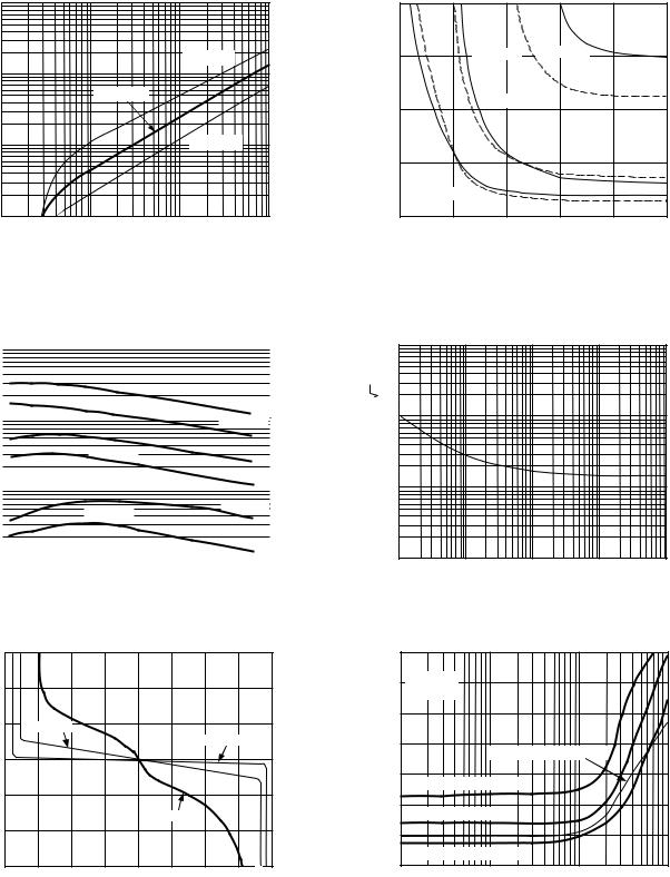
TPC 7. Open-Loop Gain vs. Load Resistance
|
10M |
|
|
|
|
|
|
|
|
|
|
|
|
|
|
|
|
|
|
|
|
|
|
|
|
|
|
|
|
|
|
|
|
|
|
|
|
|
|
|
|
|
|
|
|
|
|
|
|
|
|
|
|
|
|
|
|
|
|
|
|
|
|
|
|
|
|
|
|
|
|
|
|
|
|
|
|
|
||
|
|
|
|
RL = 100k |
|
|
|
|
|
|
|
|
|
|
|
|
|
|
|
|
|
|
||||
|
|
|
|
|
|
|
|
|
|
|
|
|
|
|
V |
= 15V |
|
|||||||||
V/V |
1M |
|
|
|
|
|
|
|
|
|
|
|
|
|
|
|
|
|
|
|
S |
|
|
|
|
|
|
|
|
|
|
|
|
|
|
|
|
|
|
|
|
|
|
|
|
|
|
|
|
|
|
||
|
|
|
|
|
|
|
|
|
|
|
|
|
|
|
|
|
|
VS = 0V, 5V |
|
|||||||
– |
|
|
|
|
|
|
|
|
|
|
|
|
|
|
|
|
|
|
|
|||||||
|
|
|
|
|
|
|
|
|
|
|
|
|
|
|
|
|
|
|
|
|||||||
GAIN |
|
|
|
|
|
|
|
|
|
|
|
|
|
|
|
|
|
|
|
|
|
|
|
|
|
|
|
|
|
|
|
|
|
|
|
R = 10k |
|
|
|
|
|
|
|
VS = 15V |
|
||||||||
OPEN-LOOP |
|
|
|
|
|
|
|
|
|
L |
|
|
|
|
|
|
|
|
|
|
|
|
|
|
|
|
|
|
|
|
|
|
|
|
|
|
|
|
|
|
|
|
|
|
|
|
|
|
|
|
|||
|
|
|
|
|
|
|
|
|
|
|
|
|
|
|
|
|
|
|
|
VS = 15V |
|
|
||||
|
|
|
|
|
|
|
|
|
|
|
|
|
|
|
|
|
|
|
|
VS |
= 0V, 5V |
|
|
|||
|
100k |
|
|
|
|
|
|
|
|
|
|
|
|
|
|
|
|
|
|
|
|
|
|
|
|
|
|
|
|
|
|
|
|
|
|
|
|
|
|
|
|
|
|
|
|
|
|
|
|
|
|
|
|
|
|
|
|
|
|
|
|
|
RL = |
600 |
|
|
|
|
|
|
|
|
|
|
|
|
|
|
|
|
|
|
|
|
|
|
|
|
|
|
|
|
|
|
|
|
|
|
|
|
|
|
|
|
|||
|
|
|
|
|
|
|
|
|
|
|
|
|
|
|
|
|
|
|
|
|
|
|
|
|||
|
|
|
|
|
|
|
|
|
|
|
|
|
|
|
|
|
|
|
|
VS = |
0V, 5V |
|
||||
|
10k |
|
|
|
|
|
|
|
|
|
|
|
|
|
|
|
|
|
|
|
|
|
|
|
|
|
|
|
–40 |
–20 |
0 |
20 |
40 |
60 |
80 |
100 |
120 |
140 |
|||||||||||||||
|
–60 |
|||||||||||||||||||||||||
TEMPERATURE – C
TPC 8. Open-Loop Gain vs. Temperature
|
300 |
|
|
|
|
|
|
|
|
|
200 |
|
|
|
|
|
|
|
|
V |
100 |
RL = 10k |
|
|
|
|
|
|
|
– |
|
|
|
|
|
|
RL = 100k |
|
|
VOLTAGE |
|
|
|
|
|
|
|
||
0 |
|
|
|
|
|
|
|
|
|
|
|
|
|
|
|
|
|
|
|
INPUT |
–100 |
|
|
|
|
|
|
|
|
|
|
|
|
|
RL = 600 |
|
|
|
|
|
|
|
|
|
|
|
|
|
|
|
–200 |
|
|
|
|
|
|
|
|
|
–300 |
|
|
|
|
|
|
|
|
|
–16 |
–12 |
–8 |
–4 |
0 |
4 |
8 |
12 |
16 |
OUTPUT VOLTAGE – V
TPC 9. Input Error Voltage vs. Output Voltage for Resistive Loads
|
40 |
|
|
|
|
|
|
|
|
R |
L |
= 20k |
RL = 2k |
POS RAIL |
|
|
20 |
|
|
||||
|
|
|
|
|
|
||
– V |
|
|
|
|
|
NEG RAIL |
|
VOLTAGE |
0 |
|
POS RAIL |
|
|
|
|
|
|
|
|
|
|
||
|
POS |
|
|
|
|
|
|
|
RAIL |
|
|
|
|
|
|
INPUT |
–20 |
|
|
|
|
NEG RAIL |
|
|
|
|
|
|
|
||
|
|
|
|
|
|
|
|
|
|
RL = 100k |
|
|
|
|
|
|
–40 |
|
|
|
|
NEG RAIL |
|
|
60 |
|
120 |
180 |
240 |
300 |
|
|
0 |
|
|||||
|
|
OUTPUT VOLTAGE FROM SUPPLY RAILS – mV |
|
||||
TPC 10. Input Error Voltage with Output Voltage within 300 mV of Either Supply Rail for Various Resistive Loads; VS = ±5 V
|
1k |
HZ |
|
– nV/ |
100 |
VOLTAGE NOISE |
10 |
INPUT |
|
1 |
10 |
100 |
1k |
10k |
1 |
FREQUENCY – Hz
TPC 11. Input Voltage Noise vs. Frequency
|
–40 |
|
|
|
|
–50 |
RL = 10k |
|
|
|
|
ACL = –1 |
|
|
|
–60 |
|
|
|
dB |
–70 |
VS = 0V, 3V; VOUT = 2.5V p-p |
|
|
|
|
|||
– |
|
|
|
|
THD |
–80 |
|
|
|
VS = 15V; VOUT = 20V p-p |
|
|
||
|
|
|
||
|
–90 |
|
|
|
|
VS = 5V; VOUT = 9V p-p |
|
|
|
|
–100 |
|
|
|
|
VS = 0V, 5V; VOUT = 4.5V p-p |
|
|
|
|
–110 |
1k |
10k |
100k |
|
100 |
|||
|
|
FREQUENCY – Hz |
|
|
TPC 12. Total Harmonic Distortion vs. Frequency
–8– |
REV. E |
|
100 |
|
|
|
|
|
|
|
|
|
|
|
|
|
|
100 |
|
|
|
|
|
|
|
|
|
|
|
|
|
|
|
|
|
||
dB–GAINLOOP-OPEN |
80 |
|
|
|
|
|
|
|
|
|
|
|
|
|
|
80 |
DEGREESINMARGINPHASE |
|
|
|
|
|
|
|
|
|
|
|
|
|
|
||||
|
|
|
|
|
|
|
|
|
|
|
|
|
|
|
|
||
|
|
|
|
|
|
|
|
|
|
|
PHASE |
|
|
|
|
||
|
60 |
|
|
|
|
|
|
|
|
|
|
|
|
|
|
60 |
|
|
|
|
|
|
|
|
|
|
|
|
|
|
|
|
|
||
|
|
|
|
|
|
|
|
|
|
|
|
|
|
|
|
|
|
|
|
|
|
|
|
|
|
GAIN |
|
|
|
|
|
|
|
|
|
|
40 |
|
|
|
|
|
|
|
|
|
|
|
|
|
|
40 |
|
|
|
|
|
|
|
|
|
|
|
|
|
|
|
|
|
||
|
20 |
|
|
|
|
|
|
|
|
|
|
|
|
|
|
20 |
|
|
|
|
|
|
|
|
|
|
|
|
|
|
|
|
|
||
|
|
|
|
|
|
|
|
|
|
|
|
|
|
|
|
|
|
|
0 |
|
RL = 2k |
|
|
|
|
|
|
|
|
|
|
|
0 |
|
|
|
|
|
|
|
|
|
|
|
|
|
|
|
|
||||
|
|
CL = 100pF |
|
|
|
|
|
|
|
|
|
|
|
||||
|
|
|
|
|
|
|
|
|
|
|
|
|
|
|
|||
|
–20 |
|
|
|
|
|
|
|
|
|
|
|
|
|
|
–20 |
|
|
|
100 |
|
1k |
|
10k |
100k |
1M |
|
|
|||||||
|
10 |
|
|
10M |
|
||||||||||||
FREQUENCY – Hz
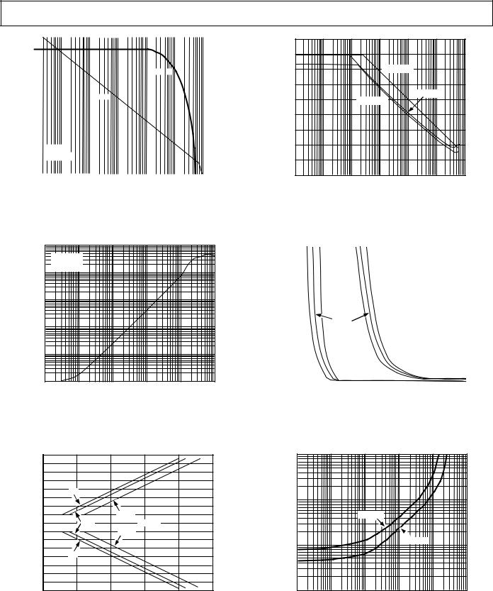
TPC 13. Open-Loop Gain and Phase Margin vs. Frequency
|
1k |
|
|
|
|
|
|
|
ACL = +1 |
|
|
|
|
|
100 |
VS = 15V |
|
|
|
|
|
|
|
|
|
|
|
– |
|
|
|
|
|
|
IMPEDANCE |
10 |
|
|
|
|
|
|
|
|
|
|
|
|
OUTPUT |
1 |
|
|
|
|
|
0.1 |
|
|
|
|
|
|
|
|
|
|
|
|
|
|
0.01 |
|
|
|
|
|
|
100 |
1k |
10k |
100k |
1M |
10M |
FREQUENCY – Hz
TPC 14. Output Impedance vs. Frequency
|
16 |
|
|
|
|
|
|
12 |
|
|
|
|
|
VOLTS |
8 |
1% |
|
|
|
|
|
|
|
|
|
||
|
|
|
|
|
|
|
0 TO |
4 |
|
|
|
|
|
|
|
|
0.01% |
|
|
|
FROM |
|
|
|
|
|
|
0 |
0.1% |
|
ERROR |
|
|
|
|
|
|
0.01% |
|
|
|
SWING |
–4 |
|
|
|
|
|
–8 |
1% |
|
|
|
|
|
OUTPUT |
|
|
|
|
||
|
|
|
|
|
||
–12 |
|
|
|
|
|
|
|
|
|
|
|
|
|
|
–16 |
1.0 |
2.0 |
3.0 |
4.0 |
5.0 |
|
0.0 |
|||||
|
|
|
SETTLING TIME – s |
|
|
|
TPC 15. Output Swing and Error vs. Settling Time
|
|
|
|
|
|
AD822 |
|
|
90 |
|
|
|
|
|
|
|
80 |
|
|
|
|
|
|
– dB |
70 |
|
|
VS = 15V |
|
|
|
REJECTION |
60 |
|
|
|
|
|
|
50 |
|
|
VS = 0V, 3V |
VS = 0V, 5V |
|
||
|
|
|
|
|
|||
|
|
|
|
|
|
|
|
COMMON-MODE |
40 |
|
|
|
|
|
|
30 |
|
|
|
|
|
|
|
20 |
|
|
|
|
|
|
|
|
|
|
|
|
|
|
|
|
10 |
|
|
|
|
|
|
|
0 |
100 |
1k |
10k |
100k |
1M |
10M |
|
10 |
||||||
|
|
|
|
FREQUENCY – Hz |
|
|
|
TPC 16. Common-Mode Rejection vs. Frequency
mV |
5 |
|
|
|
|
|
|
|
|
|
|
|
|
|
|
|
|
|
|
|
|
|
|
|
|
|
|
|
|
|
|
|
|
|
|
|
|
|
|
|
|
|
|
|
|
|
|
||
|
|
|
|
|
|
|
|
|
|
|
|
|
|
|
|
|
|
|
|
|
|
|
|
|
4 |
|
|
|
|
NEGATIVE |
|
|
|
POSITIVE |
|
|
|
|
|
|
|||||||||
– |
|
|
|
|
|
|
|
|
|
|
|
|
||||||||||||
VOLTAGE |
|
|
|
|
|
RAIL |
|
|
RAIL |
|
|
|
|
|
|
|||||||||
3 |
|
|
|
|
|
|
|
|
|
|
|
|
|
|
|
|
|
|
|
|
|
|
|
|
|
|
|
|
|
|
|
|
|
|
|
|
|
|
|
|
|
|
|
|
|
|
|
||
ERROR |
|
|
|
|
|
|
|
|
|
|
|
|
|
|
|
|
|
|
|
|
|
|
|
|
|
|
|
|
|
|
|
|
|
|
|
|
|
|
|
|
|
|
|
|
|
|
|
|
|
|
|
|
|
|
|
|
+25 C |
|
|
|
|
|
|
|
|
|
|
|
|
|||||
COMMON-MODE |
2 |
|
|
|
|
|
|
|
|
|
|
|
|
|
|
|
|
|
|
|
|
|
|
|
|
|
|
|
|
|
|
|
|
|
|
|
|
|
|
|
|
|
|
|
|
|
|
||
|
|
|
|
|
|
|
|
|
|
|
|
|
|
|
|
|
|
|
|
|
|
|
|
|
|
|
|
|
|
|
|
|
|
|
|
|
|
|
|
|
|
+125 C |
|
|
|
|
|||
|
1 |
|
|
|
|
|
–55 C |
|
|
|
|
|
|
|
|
|
|
|
|
|||||
|
|
|
|
|
|
|
|
|
|
|
|
|
|
|
|
|
|
|||||||
|
|
|
|
|
|
|
|
|
|
|
|
|
|
|
|
|
|
|
|
|
|
|
|
|
|
|
|
|
|
|
|
|
|
|
|
|
|
|
–55 C |
|
|
|
|
|
|
|
|
|
|
|
|
|
|
|
|
|
|
|
|
|
|
|
|
|
|
|
|
|
|
|
|
|
|
|
|
|
|
+125 C |
|
|
|
|
|
|
|
|
|
|
|
|
|
|
|
|
|
|
|
||
|
0 |
|
|
|
|
|
|
|
|
|
|
|
|
|
|
|
|
|
|
|
|
|
|
|
|
|
0 |
|
|
|
|
1 |
|
|
|
2 |
3 |
||||||||||||
|
–1 |
|
|
|
|
|
|
|
||||||||||||||||
COMMON-MODE VOLTAGE FROM SUPPLY RAILS – V
TPC 17. Absolute Common-Mode Error vs. Com- mon-Mode Voltage from Supply Rails (VS – VCM)
|
1000 |
|
|
|
|
|
– mV |
|
|
|
|
|
|
VOLTAGE |
100 |
|
|
|
|
|
|
|
VS – VOH |
|
|
|
|
OUTPUT SATURATION |
10 |
|
|
|
VOL – VS |
|
|
|
|
|
|
|
|
|
0 |
0.01 |
0.1 |
1 |
10 |
100 |
|
0.001 |
LOAD CURRENT – mA
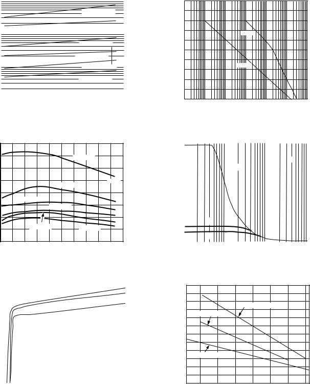
TPC 18. Output Saturation Voltage vs. Load Current
REV. E |
–9– |
AD822
|
1000 |
|
|
|
|
|
|
|
|
|
|
|
|
|
|
|
|
|
|
|
|
|
|
|
|
|
|
|
|
|
|
|
|
|
|
|
|
|
|
|
|
|
|
|
|
|
|
|
|
|
|
|
|
|
|
|
|
|
|
|
|
|
|
|
|
|
|
|
|
|
|
|
|
|
|
||
– mV |
|
|
|
|
|
|
|
|
|
|
|
|
|
|
|
ISOURCE = 10mA |
|
|
|
||||||
|
|
|
|
|
|
|
|
|
|
|
|
|
|
|
|
|
|
|
|
|
|
|
|
|
|
VOLTAGE |
|
|
|
|
|
|
|
|
|
|
|
|
|
|
|
|
|
|
|
|
|
|
|
|
|
|
|
|
|
|
|
|
|
|
|
|
|
|
|
|
ISINK = 10mA |
|
|
|
|
|
|
||||
|
100 |
|
|
|
|
|
|
|
|
|
|
|
|
|
|
|
|
|
|
|
|
|
|
|
|
|
|
|
|
|
|
|
|
|
|
|
|
|
|
|
|
|
|
|
|
|
|
|
|
|
|
|
|
|
|
|
|
|
|
|
|
|
|
|
|
|
|
|
|
|
|
|
|
|
|
||
SATURATION |
|
|
|
|
|
|
|
|
|
|
|
|
|
|
|
ISOURCE = 1mA |
|
|
|
||||||
10 |
|
|
|
|
|
|
|
|
|
|
|
|
|
|
|
|
|
|
A |
|
|
||||
|
|
|
|
|
|
|
|
|
|
|
|
|
|
ISOURCE = 10 |
|
|
|||||||||
|
|
|
|
|
|
|
|
|
|
|
|
|
|
|
|
ISINK = 1mA |
|
|
|
|
|
|
|||
OUTPUT |
|
|
|
|
|
|
|
|
|
|
|
|
|
|
|
|
|
|
|
|
|
|
|
|
|
|
|
|
|
|
|
|
|
|
|
|
|
|
|
|
|
|
|
|
|
|
|
|
|
|
|
|
|
|
|
|
|
|
|
|
|
|
|
|
|
|
ISINK = 10 A |
|
|
|
|
|
|
||||
|
1 |
|
|
|
|
|
|
|
|
|
|
|
|
|
|
|
|
|
|
|
|
|
|
|
|
|
|
|
|
–20 |
0 |
20 |
40 |
60 |
|
|
80 |
100 |
120 |
|
|
|
|||||||||
|
–60 |
–40 |
|
|
|
140 |
|||||||||||||||||||
TEMPERATURE – C
TPC 19. Output Saturation Voltage vs. Temperature
|
80 |
|
|
|
|
|
|
|
|
|
|
|
70 |
|
|
|
|
|
VS = |
15V |
|
|
|
|
|
|
|
|
|
|
|
|
|
||
mA |
60 |
|
|
|
|
|
|
|
|
|
|
– |
|
|
|
|
|
|
|
|
|
|
|
LIMIT |
50 |
|
|
|
|
VS = 15V |
|
|
–OUT |
|
|
|
|
|
|
|
|
|
|
||||
|
|
|
|
|
|
|
|
|
|||
CURRENT |
|
|
|
|
|
|
|
|
|
||
40 |
|
|
|
|
|
|
|
|
|
|
|
30 |
|
VS = 0V, 5V |
|
|
|
|
|
+ |
|
||
|
|
|
VS = 0V, 3V |
|
|
|
|
|
|||
CIRCUIT |
|
|
|
|
|
|
|
– |
|
||
20 |
|
|
|
|
|
|
|
|
– |
|
|
|
|
|
|
|
|
|
|
+ |
|
||
|
|
|
|
|
|
|
|
|
|
||
SHORT |
10 |
|
VS |
= 0V, 5V |
|
VS = 0V, 3V |
+ |
|
|||
|
|
|
|
|
|
|
|||||
0 |
|
|
|
|
|
|
|
|
|
|
|
|
–40 |
–20 |
0 |
20 |
40 |
60 |
80 |
100 |
120 |
140 |
|
|
–60 |
||||||||||
|
|
|
|
|
TEMPERATURE – C |
|
|
|
|
||
TPC 20. Short Circuit Current Limit vs. Temperature
|
1600 |
|
|
|
|
|
|
|
|
|
|
|
|
|
|
|
|
|
|
|
|
|
|
|
|
|
|
|
|
|
|
|
|
|
|
|
|
|
|
|
|
|
|
|
|
|
|
|
|
|
|
|
|
|
T = |
+125 C |
|
|
|
|
|
|
|
||
|
1400 |
|
|
|
|
|
|
|
|
|
|
|
|
|
|
|
|
|
|
|
|
|
|
|
|
|
|
|
|
|
|
|
|
|
|
|
|
|
|
|
|
|
|
|
|
|
|
|
|
|
|
|
|
|
|
T |
= +25 C |
|
|
|
|
|
|
||
A |
1200 |
|
|
|
|
|
|
|
|
|
|
|
|
|
|
|
|
|
|
|
|
– |
|
|
|
|
|
|
|
|
|
|
|
|
|
|
|
|
|
|
|
|
|
|
|
|
|
|
|
|
|
|
|
T = |
–55 C |
|
|
|
|
|
|
|
|
||
CURRENT |
800 |
|
|
|
|
|
|
|
|
|
|
|
|
|
|
|
|
|
|
|
|
QUIESCENT |
1000 |
|
|
|
|
|
|
|
|
|
|
|
|
|
|
|
|
|
|
|
|
600 |
|
|
|
|
|
|
|
|
|
|
|
|
|
|
|
|
|
|
|
|
|
|
|
|
|
|
|
|
|
|
|
|
|
|
|
|
|
|
|
|
|
||
|
|
|
|
|
|
|
|
|
|
|
|
|
|
|
|
|
|
|
|
|
|
|
400 |
|
|
|
|
|
|
|
|
|
|
|
|
|
|
|
|
|
|
|
|
|
|
|
|
|
|
|
|
|
|
|
|
|
|
|
|
|
|
|
|
|
|
|
200 |
|
|
|
|
|
|
|
|
|
|
|
|
|
|
|
|
|
|
|
|
|
|
|
|
|
|
|
|
|
|
|
|
|
|
|
|
|
|
|
|
|
|
|
0 |
|
|
|
|
|
|
|
|
|
|
|
|
|
|
|
|
|
|
|
|
|
|
4 |
8 |
12 |
16 |
20 |
24 |
28 |
32 |
36 |
|||||||||||
|
0 |
||||||||||||||||||||
TOTAL SUPPLY VOLTAGE – V
TPC 21. Quiescent Current vs. Supply Voltage vs. Temperature
|
100 |
|
|
|
|
|
|
|
90 |
|
|
|
|
|
|
– dB |
80 |
|
|
|
|
|
|
70 |
|
|
|
|
|
|
|
REJECTION |
|
|
+PSRR |
|
|
|
|
|
|
|
|
|
|
||
60 |
|
|
|
|
|
|
|
50 |
|
|
|
|
|
|
|
|
|
|
|
|
|
|
|
SUPPLY |
40 |
|
|
|
|
|
|
30 |
|
|
–PSRR |
|
|
|
|
|
|
|
|
|
|
||
POWER |
20 |
|
|
|
|
|
|
10 |
|
|
|
|
|
|
|
|
|
|
|
|
|
|
|
|
0 |
100 |
1k |
10k |
100k |
1M |
10M |
|
10 |
||||||
|
|
|
|
FREQUENCY – Hz |
|
|
|
TPC 22. Power Supply Rejection vs. Frequency
|
30 |
|
|
|
|
|
|
|
|
|
|
|
|
|
|
|
|
|
|
|
|
|
|
|
|
|
|
|
|
|
|
|
|
|
|
|
25 |
|
|
|
|
|
|
|
RL = 2k |
|
|
|
|
|
|
|
|
|
|
|
|
||
|
|
|
|
|
VS = 15V |
|
|
|
|
|
|
V |
20 |
|
|
|
|
|
|
|
|
|
|
– |
|
|
|
|
|
|
|
|
|
|
|
|
|
|
|
|
|
|
|
|
|
|
|
VOLTAGE |
15 |
|
|
|
|
|
|
|
|
|
|
OUTPUT |
10 |
|
|
|
|
|
|
|
|
|
|
|
|
|
|
|
|
|
|
|
|
|
|
|
|
|
|
|
|
|
|
|
|
||
|
5 |
|
VS = 0V, 5V |
|
|
|
|
|
|
|
|
|
|
|
|
|
|
|
|
|
|
|
|
|
|
|
|
|
|
|
|
|
|
|
|
|
|
|
VS = 0V, 3V |
|
|
|
|
|
|
|
|
|
0 |
|
|
|
|
|
|
|
|
|
|
|
|
|
100k |
1M |
|
10M |
|||||
|
10k |
|
|
||||||||
FREQUENCY – Hz
TPC 23. Large Signal Frequency Response
|
2.4 |
|
|
|
|
|
|
|
|
2.2 |
|
|
|
|
|
|
|
W |
2.0 |
|
|
|
8-LEAD PDIP |
|
|
|
|
|
|
|
|
|
|||
– |
1.8 |
|
|
|
|
|
||
|
|
|
|
|
|
|
||
DISSIPATION |
8-LEAD SOIC |
|
|
|
|
|
||
1.6 |
|
|
|
|
|
|||
|
|
|
|
|
|
|
||
1.4 |
|
|
|
|
|
|
|
|
1.2 |
|
|
|
|
|
|
|
|
POWER |
1.0 |
|
|
|
|
|
|
|
0.8 |
8-LEAD MSOP |
|
|
|
|
|
||
TOTAL |
0.6 |
|
|
|
|
|
||
|
|
|
|
|
|
|
||
0.4 |
|
|
|
|
|
|
|
|
|
|
|
|
|
|
|
|
|
|
0.2 |
|
|
|
|
|
|
|
|
0.0 |
|
–20 |
0 |
20 |
40 |
60 |
80 |
|
–60 |
–40 |
||||||
|
|
|
AMBIENT TEMPERATURE – C |
|
|
|||
TPC 24. Maximum Power Dissipation vs. Temperature for Plastic Packages
–10– |
REV. E |
AD822
|
–70 |
|
|
|
|
|
|
|
|
–80 |
|
|
|
|
|
|
|
|
–90 |
|
|
|
|
|
|
|
– dB |
–100 |
|
|
|
|
|
|
|
CROSSTALK |
|
|
|
|
|
|
|
|
–110 |
|
|
|
|
|
|
|
|
–120 |
|
|
|
|
|
|
|
|
|
|
|
|
|
|
|
|
|
|
–130 |
|
|
|
|
|
|
|
|
–140 |
1k |
3k |
10k |
30k |
100k |
300k |
1M |
|
300 |
FREQUENCY – Hz
TPC 25. Crosstalk vs. Frequency
VOUT
+VS
20k 2.2k
|
0.1 F |
1 F |
|
|
8 |
1/2 |
|
2 |
AD822 |
6 |
20V p-p |
1 |
|
7 |
|
3 |
5k |
5 |
|
1/2 |
5k |
|
|
AD822 |
|
|
VIN |
0.1 F |
1 F |
|
VOUT |
|||
|
|
||
CROSSTALK = 20LOG 10VIN |
–V |
|
|
|
S |
|
TPC 28. Crosstalk Test Circuit
5V |
|
5µs |
1/2 |
+VS |
0.01 F |
100 |
AD822 |
|
90 |
|
|
|
||
|
8 |
|
|
VIN |
|
|
VOUT |
|
|
RL |
|
|
|
100pF |
|
|
4 |
0.01 F |
|
|
|
|
10 |
|
|
|
0% |
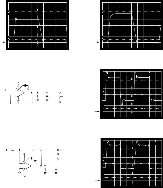
TPC 26. Unity Gain Follower |
TPC 29. Large Signal Response Unity Gain Follower; |
|
VS = ±15 V, RL = 10 kΩ |
5V |
10µs |
10mV |
500ns |
100 |
100 |
90 |
90 |
10 |
10 |
0% |
0% |
TPC 27. 20 V p-p, 25 kHz Sine Wave Input; Unity |
TPC 30. Small Signal Response Unity Gain Follower; |
Gain Follower; RL = 600 Ω, VS = ±15 V |
VS = ±15 V, RL = 10 kΩ |
REV. E |
–11– |
AD822
1V |
2µs |
1V |
2µs |
|
100 |
100 |
|
90 |
90 |
|
10 |
10 |
GND |
0% |
GND 0% |
TPC 31. VS = 5 V, 0 V; Unity Gain Follower Response |
TPC 34. VS = 5 V, 0 V; Unity Gain Follower Response |
to 0 V to 4 V Step |
to 0 V to 5 V Step |
|
|
|
|
10mV |
2µs |
+VS |
|
|
|
100 |
|
0.01 F |
|
|
90 |
|
|
|
|
|
|
||
8 |
|
|
|
|
|
VIN |
|
|
|
|
|
|
1/2 |
RL |
VOUT |
|
|
4 |
AD822 |
100pF |
|
|
|
|
|
|
|
|
|
|
|
|
|
10 |
|
|
|
|
GND |
0% |
|
TPC 32. Unity Gain Follower |
TPC 35. VS = 5 V, 0 V; Unity Gain Follower Response, to |
|
40 mV Step Centered 40 mV above Ground, RL = 10 kΩ |
10k |
|
20k |
|
|
VIN |
+VS |
|
|
VOUT |
|
|
|
||
|
|
0.01 F |
|
|
|
8 |
|
|
|
|
|
1/2 |
RL |
100pF |
|
4 |
AD822 |
||
|
|
|
|
TPC 33. Gain-of-T2 Inverter
10mV |
|
2µs |
100
90
10
GND 0%
TPC 36. VS = 5 V, 0 V; Gain-of-2 Inverter Response to 20 mV Step, Centered 20 mV below Ground, RL = 10 kΩ
–12– |
REV. E |