


LTC1418
BLOCK DIAGRAM
|
|
|
CSAMPLE |
|
AIN+ |
|
|
|
|
|
|
|
CSAMPLE |
VDD: 5V |
|
|
|
VSS: 0V FOR UNIPOLAR MODE |
|
AIN– |
|
|
|
|
8k |
|
|
–5V FOR BIPOLAR MODE |
|
2.5V |
2.5V REF |
|
ZEROING SWITCHES |
|
VREF |
|
|
|
|
|
|
|
|
|
REF AMP |
|
|
|
|
|
|
|
|
|
|
|
|
|
|
|
|
+ |
COMP |
|
|
|
|
|
|
|
|
|
|
|
|
|
|
|
|
|
|
|
|
14-BIT CAPACITIVE DAC |
|
|
|
|
|
|
|
|
|
|||||||||||
|
|
|
|
|
|
|
|
|
|
|
|
|
|
|
|
|
|
|
|
|
|
|||||||||||
|
|
|
|
|
|
|
|
|
|
|
|
|
|
|
|
|
|
|
|
|
|
|||||||||||
REFCOMP |
|
|
4.096V |
|
|
|
|
|
|
|
|
|
|
|
|
|
|
|
|
– |
|
|
|
|
|
|
|
|||||
|
|
|
|
|
|
|
|
|
|
|
|
|
|
|
|
|
|
|
|
|
|
|
|
|
||||||||
|
|
|
|
|
|
|
|
|
|
|
|
|
|
|
|
|
|
|
|
|
|
|
|
|
|
|
||||||
|
|
|
|
|
|
|
|
|
|
|
|
|
|
|
|
|
|
|
|
|
|
|
|
|
|
|
||||||
|
|
|
|
|
|
|
|
|
|
|
|
|
|
14 |
|
|
|
|
|
|
D13 |
|||||||||||
|
|
|
|
|
|
|
|
|
|
|
|
|
|
|
|
|
|
|
|
|
|
|
|
|
|
|
||||||
|
|
|
|
|
|
|
|
|
|
|
|
|
|
|
|
|
|
|
|
|
|
|
|
|
|
|
||||||
|
|
|
|
|
|
|
|
|
|
|
|
|
SUCCESSIVE APPROXIMATION |
|
|
|
|
|
SHIFT |
|
• |
|||||||||||
|
|
|
|
|
|
|
|
|
|
|
|
|
|
|
REGISTER |
|
|
|
|
REGISTER |
|
• |
|
|
||||||||
|
|
|
|
|
|
|
|
|
|
|
|
|
|
|
|
|
|
|
|
|
||||||||||||
AGND |
|
|
|
|
|
|
|
|
|
|
|
|
|
|
|
|
|
|
|
• |
|
D0 |
||||||||||
|
|
|
|
|
|
|
|
|
|
|
|
|
|
|
|
|
|
|
|
|
|
|
|
|
|
|
|
|
|
|
|
D3/(SCLK) |
DGND |
|
|
|
INTERNAL |
|
|
|
MUX |
|
|
|
CONTROL LOGIC |
|
|
|
|
|
|
|
|
|
|
D1/(DOUT) |
|||||||||
|
|
|
CLOCK |
|
|
|
|
|
|
|
|
|
|
|
|
|
|
|
|
|||||||||||||
|
|
|
|
|
|
|
|
|
|
|
|
|
|
|
|
|
|
|
|
|
|
|
|
|
|
|
|
|
|
|||
|
|
|
|
|
|
|
|
|
|
|
|
|
|
|
|
|
|
|
|
|
|
|
|
|
|
|
|
|
|
|
|
|
|
|
|
|
|
|
|
|
|
|
|
|
|
|
|
|
|
|
|
|
|
|
|
|
|
|
|
|
|
1418 BD |
|
|
|
|
|
|
|
|
D4 (EXTCLKIN) |
D0 (EXT/INT) |
SHDN CONVST RD CS SER/PAR D2/(CLKOUT) BUSY |
|
|
|
|
|
||||||||||||||||||||
|
|
|
|
|
|
|
|
|
|
|
|
|||||||||||||||||||||
NOTE: PIN NAMES IN PARENTHESES
REFER TO SERIAL MODE
APPLICATIONS INFORMATION
CONVERSION DETAILS
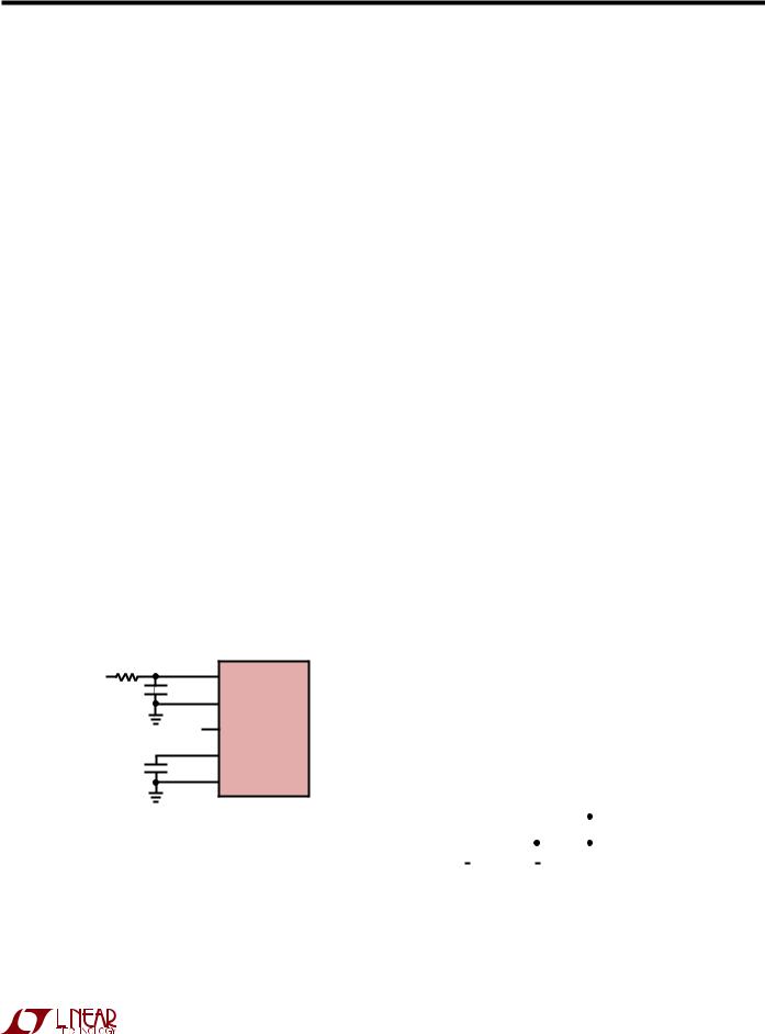
The LTC1418 uses a successive approximation algorithm and an internal sample-and-hold circuit to convert an analog signal to a 14-bit parallel or serial output. The ADC is complete with a precision reference and an internal clock. The control logic provides easy interface to microprocessors and DSPs (please refer to Digital Interface section for the data format).
Conversion start is controlled by the CS and CONVST inputs. At the start of the conversion the successive approximation register (SAR) is reset. Once a conversion cycle has begun it cannot be restarted.
During the conversion, the internal differential 14-bit capacitive DAC output is sequenced by the SAR from the most significant bit (MSB) to the least significant bit (LSB).
|
SAMPLE |
CSAMPLE+ |
|
|
|
|
AIN+ |
|
|
|
|
|
|
|
HOLD |
|
ZEROING SWITCHES |
|
||
|
|
|
|
|||
|
SAMPLE |
CSAMPLE– |
|
|
HOLD |
|
AIN– |
|
|
|
|
|
|
|
HOLD |
|
|
HOLD |
|
|
|
|
|
|
|
||
|
|
CDAC+ |
|
|
|
|
|
|
|
|
+ |
|
|
|
VDAC+ |
CDAC– |
|
COMP |
|
|
|
|
|
– |
|
|
|
|
|
|
|
|
|
|
|
|
VDAC– |
SAR |
14 |
OUTPUT |
D13 |
|
|
|
|
LATCH |
D0 |
|
|
|
|
|
|
||
|
|
|
|
|
|
|
|
|
|
|
|
|
1418 F01 |
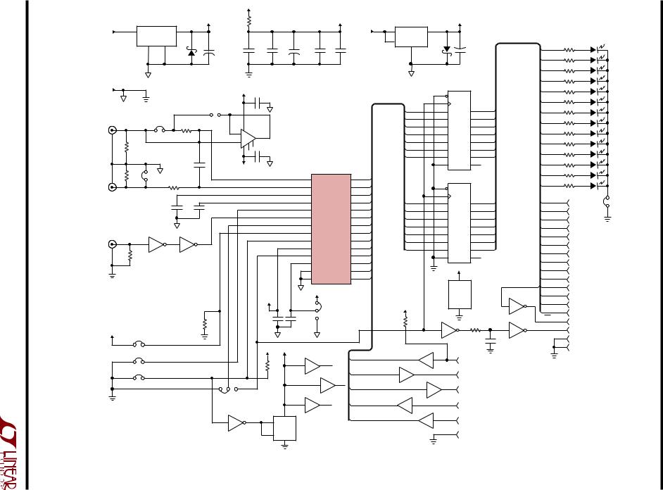
Figure 1. Simplified Block Diagram
|
|
1418fa |
|
|
|
|
|
|
|
For more information www.linear.com/LTC1418 |
9 |
|
||
|

LTC1418
APPLICATIONS INFORMATION
ReferringtoFigure 1,theAIN+ andAIN– inputsareconnected
to the sample-and-hold capacitors (CSAMPLE) during the acquire phase and the comparator offset is nulled by the
zeroing switches. In this acquire phase, a minimum delay of 1µs will provide enough time for the sample-and-hold capacitors to acquire the analog signal. During the convert phase, the comparator zeroing switches open, putting the comparator into compare mode. The input switches the CSAMPLE capacitors to ground, transferring the differential analog input charge onto the summing junction. This input charge is successively compared with the binary weighted charges supplied by the differential capacitive DAC. Bit decisions are made by the high speed comparator. At the end of a conversion, the differential DAC output balances the AIN+ and AIN– input charges. The SAR contents (a 14 bit data word) which represent the difference of AIN+ and AIN– are loaded into the 14-bit output latches.
DYNAMIC PERFORMANCE
The LTC1418 has excellent high speed sampling capability. FFT (Fast Fourier Transform) test techniques are used to test the ADC’s frequency response, distortion and noise at the rated throughput. By applying a low distortion sine wave and analyzing the digital output using an FFT algorithm, the ADC’s spectral content can be examined for frequencies outside the fundamental. Figure 2a shows a typical LTC1418 FFT plot.
Signal-to-Noise Ratio
The signal-to-noise plus distortion ratio [S/(N + D)] is the ratio between the RMS amplitude of the fundamental input frequency to the RMS amplitude of all other frequency components at the A/D output. The output is band limited to frequencies from above DC and below half the sampling frequency. Figure 2b shows a typical spectral content with a 200kHz sampling rate and a 10kHz input. The dynamic performance is excellent for input frequencies up to and beyond the Nyquist limit of 100kHz.
|
0 |
|
|
|
|
|
|
|
|
|
|
|
fSAMPLE = 200kHz |
|
|
–20 |
|
fIN = 9.9609375kHz |
|
|
|
SFDR = 99.32 |
|
|
|
|
|
|
|
|
|
|
SINAD = 82.4 |
|
(dB) |
–40 |
|
|
|
|
|
|
||
|
|
|
|
|
AMPLITUDE |
–60 |
|
|
|
|
|
|
|
|
|
–80 |
|
|
|
|
|
|
|
–100
–120 0 10 20 30 40 50 60 70 80 90 100 FREQUENCY (kHz)
1418 F02a
Figure 2a. LTC1418 Nonaveraged, 4096 Point FFT, Input Frequency = 10kHz
|
0 |
|
|
|
|
|
|
|
|
|
|
|
fSAMPLE = 200kHz |
|
|
–20 |
|
fIN = 97.509765kHz |
|
|
|
|||
|
|
|
SFDR = 94.29 |
|
|
|
|
SINAD = 81.4 |
|
(dB) |
–40 |
|
|
|
|
|
|
||
|
|
|
|
|
AMPLITUDE |
–60 |
|
|
|
|
|
|
|
|
|
–80 |
|
|
|
|
|
|
|
–100
–120 0 10 20 30 40 50 60 70 80 90 100 FREQUENCY (kHz)
1418 F02b
Figure 2b. LTC1418 Nonaveraged, 4096 Point FFT, Input Frequency = 97.5kHz
Effective Number of Bits
The effective number of bits (ENOBs) is a measurement of the resolution of an ADC and is directly related to the S/(N + D) by the equation:
N = [S/(N + D) – 1.76]/6.02
where N is the effective number of bits of resolution and S/(N + D) is expressed in dB. At the maximum sampling rate of 200kHz, the LTC1418 maintains near ideal ENOBs up to the Nyquist input frequency of 100kHz (refer to Figure 3).
|
|
|
1418fa |
|
|
||
|
|
|
|
10 |
For more information www.linear.com/LTC1418 |
|
|
|
|
||
|
|||
APPLICATIONS INFORMATION
|
14 |
|
|
|
|
|
|
|
|
|
|
|
|
|
|
|
|
|
|
|
|
|
|
|
|
|
|
|
|
|
|
|
|
|
|
|
|
|
|
|
|
|
|
|
|
|
|
|
|
|
|
|
|
|
|
|
13 |
|
|
|
|
|
|
|
|
|
|
|
|
|
|
|
|
|
|
|
|
|
|
|
|
|
|
|
|
|
|
|
|
|
|
|
|
|
|
|
|
|
|
|
|
|
|
|
|
|
|
|
|
|
|
|
12 |
|
|
|
|
|
|
|
|
|
|
|
|
|
|
|
|
|
|
|
|
|
|
|
|
|
|
|
|
|
|
|
|
|
|
|
|
|
|
|
|
|
|
|
|
|
|
|
|
|
|
|
|
|
|
|
11 |
|
|
|
|
|
|
|
|
|
|
|
|
|
|
|
|
|
|
|
|
|
|
|
|
|
|
|
|
|
|
|
|
|
|
|
|
|
|
|
|
|
|
|
|
|
|
|
|
|
|
|
|
|
|
BITS |
10 |
|
|
|
|
|
|
|
|
|
|
|
|
|
|
|
|
|
|
|
|
|
|
|
|
|
|
|
|
|
|
|
|
|
|
|
|
|
|
|
|
|
|
|
|
|
|
|
|
|
|
|
|
||
9 |
|
|
|
|
|
|
|
|
|
|
|
|
|
|
|
|
|
|
|
|
|
|
|
|
|
|
|
|
|
|
|
|
|
|
|
|
|
|
|
|
|
|
|
|
|
|
|
|
|
|
|
|
|
||
EFECTIVE |
8 |
|
|
|
|
|
|
|
|
|
|
|
|
|
|
|
|
|
|
|
|
|
|
|
|
|
|
|
|
|
|
|
|
|
|
|
|
|
|
|
|
|
|
|
|
|
|
|
|
|
|
|
|
|
|
|
7 |
|
|
|
|
|
|
|
|
|
|
|
|
|
|
|
|
|
|
|
|
|
|
|
|
|
|
|
|
|
|
|
|
|
|
|
|
|
|
|
|
|
|
|
|
|
|
|
|
|
|
|
|
|
|
|
6 |
|
|
|
|
|
|
|
|
|
|
|
|
|
|
|
|
|
|
|
|
|
|
|
|
|
|
|
|
|
|
|
|
|
|
|
|
|
|
|
|
|
|
|
|
|
|
|
|
|
|
|
|
|
|
|
5 |
|
|
|
|
|
|
|
|
|
|
|
|
|
|
|
|
|
|
|
|
|
|
|
|
|
|
|
|
|
|
|
|
|
|
|
|
|
|
|
|
|
|
|
|
|
|
|
|
|
|
|
|
|
|
|
4 |
|
|
|
|
|
|
|
|
|
|
|
|
|
|
|
|
|
|
|
|
|
|
|
|
|
|
|
|
|
|
|
|
|
|
|
|
|
|
|
|
|
|
|
|
|
|
|
|
|
|
|
|
|
|
|
3 |
|
|
|
|
|
|
|
|
|
|
|
|
|
|
|
|
|
|
|
|
|
|
|
|
|
|
|
|
|
|
|
|
|
|
|
|
|
|
|
|
|
|
|
|
|
|
|
|
|
|
|
|
|
|
|
2 |
|
|
|
|
|
|
|
|
|
|
|
|
|
|
|
|
|
|
|
|
|
|
|
|
|
|
|
1k |
|
|
10k |
100k |
|
|
|
1M |
||||||||||||||||||
|
|
|
|
|
|
|
INPUT FREQUENCY (Hz) |
|
|
|
|
|
|
||||||||||||||
|
|
|
|
|
|
|
|
|
|
|
|
|
|
|
|
|
|
|
|
|
|
1418 F03 |
|||||
Figure 3. Effective Bits and Signal/(Noise + Distortion) vs Input Frequency
Total Harmonic Distortion
Total harmonic distortion (THD) is the ratio of the RMS sum of all harmonics of the input signal to the fundamental itself. The out-of-band harmonics alias into the frequency band between DC and half the sampling frequency. THD is expressed as:
THD =20Log 
 V22 +V32 +V42 +...VN2 V1
where V1 is the RMS amplitude of the fundamental frequency and V2 through VN are the amplitudes of the second through nth harmonics. THD vs Input Frequency is shown in Figure 4. The LTC1418 has good distortion performance up to the Nyquist frequency and beyond.
FUNDAMENTAL) |
0 |
|
|
|
|
|
|
|
|
|
|
|
|
|
|
|
|
|
|
|
|
|
|
|
|
|
|
|
|
|
|
|
|
|
|
|
|
|
|
|
|
|
|
|
|
|
|
|
|
|
|
|
|
|
|
|
|
|
|
|
|
|
|
||
–40 |
|
|
|
|
|
|
|
|
|
|
|
|
|
|
|
|
|
|
|
|
|
|
|
|
|
|
|
|
|
|
|
|
THE |
–20 |
|
|
|
|
|
|
|
|
|
|
|
|
|
|
|
|
|
|
|
|
|
|
|
|
|
|
|
|
|
|
|
|
|
|
|
|
|
|
|
|
|
|
|
|
|
|
|
|
|
|
|
|
|
|
|
|
|
|
|
|
|
|
|
|
|
|
|
|
|
|
|
|
|
|
|
|
|
|
|
|
|
|
|
|
|
|
|
|
|
|
|
|
|
|
|
|
|
BELOW |
–60 |
|
|
|
|
|
|
|
|
|
|
|
|
|
|
|
|
|
|
|
|
|
|
|
|
|
|
|
|
|
|
|
|
|
|
|
|
|
|
|
|
|
|
|
|
|
|
|
|
|
|
|
|
|
|
|
|
|
|
|
|
|
|
||
|
|
|
|
|
|
|
|
|
|
|
|
|
|
|
|
|
|
|
|
|
|
|
|
|
|
|
|
|
|
|
|
|
|
|
|
|
|
|
|
|
|
|
|
|
|
|
|
|
|
3RD |
|
|
|
|
|
|
|
|
|
|
|||||
(dB |
–80 |
|
|
|
|
|
|
|
|
|
|
|
|
|
|
|
|
|
|
|
|
|
|
|
|
|
|
|||||
|
|
|
|
|
|
|
|
|
|
|
|
|
|
|
|
|
|
|
|
|
|
|
|
|
|
|
|
|
|
|
||
|
|
|
|
|
|
|
|
|
|
|
|
|
|
THD |
|
|
|
|
|
|
|
|
|
|
|
|
|
|
||||
AMPLITUDE |
|
|
|
|
|
|
|
|
|
|
|
|
|
|
|
|
|
|
|
|
|
|
|
|
|
|
|
|
||||
|
|
|
|
|
|
|
|
|
|
|
|
|
|
|
|
|
|
|
|
|
|
|
|
|
|
|
|
|
|
|
|
|
|
–100 |
|
|
|
|
|
|
|
|
|
|
|
|
|
|
|
|
|
|
|
|
|
|
|
2ND |
|
|
|
|
|
||
|
|
|
|
|
|
|
|
|
|
|
|
|
|
|
|
|
|
|
|
|
|
|
|
|
|
|
|
|
|
|
|
|
|
–120 1k |
|
|
|
|
|
|
|
|
|
|
|
|
|
|
|
|
|
|
|
|
|
|
|
|
|
|
|
|
|
|
|
|
|
|
|
|
|
10k |
|
|
|
|
|
100k |
|
|
|
|
|
|
1M |
|||||||||||||
|
|
|
|
|
|
|
|
|
INPUT FREQUENCY (Hz) |
|
|
|
|
|
|
|
|
|
||||||||||||||
|
|
|
|
|
|
|
|
|
|
|
|
|
|
|
|
|
|
|
|
|
|
|
|
|
|
|
1418 F04 |
|||||
Figure 4. Distortion vs Input Frequency
LTC1418
Intermodulation Distortion
If the ADC input signal consists of more than one spectral component, the ADC transfer function nonlinearity can produce intermodulation distortion (IMD) in addition to THD. IMD is the change in one sinusoidal input caused by the presence of another sinusoidal input at a different frequency.
If two pure sine waves of frequencies fa and fb are applied to the ADC input, nonlinearities in the ADC transfer function can create distortion products at the sum and difference frequencies of mfa ±nfb, where m and n = 0, 1, 2, 3, etc. For example, the 2nd order IMD terms include (fa + fb). If the two input sine waves are equal in magnitude, the value (in decibels) of the 2nd order IMD products can be expressed by the following formula:
IMD (fa +fb)=20Log Amplitude at (fa + fb) |
|||||||||||||
|
|
|
|
|
|
Amplitude at fa |
|
|
|||||
|
0 |
|
|
|
|
|
|
|
|
|
|
|
|
|
|
|
|
|
|
|
|
|
|
|
|
|
|
|
|
|
fSAMPLE = 200kHz |
|
|
|
|
|
|
|
|||
|
–20 |
|
fIN1 |
= 97.65625kHz |
|
|
|
|
|
|
|
||
|
|
fIN2 |
= 104.248046kHz |
|
|
|
|
|
|
||||
|
|
|
|
|
|
|
|
|
|||||
(dB) |
–40 |
|
|
|
|
|
|
|
|
|
|
|
|
|
|
|
|
|
|
|
|
|
|
|
|
||
|
|
|
|
|
|
|
|
|
|
|
|
|
|
AMPLITUDE |
–80 |
|
|
|
|
|
|
|
|
|
|
|
|
|
–60 |
|
|
|
|
|
|
|
|
|
|
|
|
|
–100 |
|
|
|
|
|
|
|
|
|
|
|
|
|
|
|
|
|
|
|
|
|
|
|
|
|
|
|
|
|
|
|
|
|
|
|
|
|
|
|
|
|
–120 0 |
|
|
|
|
|
60 |
70 |
|
|
|
|
|
|
10 |
20 |
30 |
40 |
50 |
80 |
90 |
100 |
|||||
|
|
|
|
|
FREQUENCY (kHz) |
|
|
|
|
||||
|
|
|
|
|
|
|
|
|
|
|
1418 F05 |
||
Figure 5. Intermodulation Distortion Plot
Peak Harmonic or Spurious Noise
The peak harmonic or spurious noise is the largest spectral component excluding the input signal and DC. This value is expressed in decibels relative to the RMS value of a full-scale input signal.
|
|
1418fa |
|
|
|
|
|
|
|
For more information www.linear.com/LTC1418 |
11 |
|
||
|

LTC1418
APPLICATIONS INFORMATION
Full-Power and Full-Linear Bandwidth
The full-power bandwidth is that input frequency at which the amplitude of the reconstructed fundamental is reduced by 3dB for a full-scale input signal.
The full-linear bandwidth is the input frequency at which the S/(N + D) has dropped to 77dB (12.5 effective bits). The LTC1418 has been designed to optimize input bandwidth, allowing the ADC to undersample input signals with frequencies above the converter’s Nyquist Frequency. The noise floor stays very low at high frequencies; S/(N + D) becomes dominated by distortion at frequencies far beyond Nyquist.
DRIVING THE ANALOG INPUT
The differential analog inputs of the LTC1418 are easy to drive. The inputs may be driven differentially or as a single-ended input (i.e., the AIN– input is grounded). The AIN+ and AIN– inputs are sampled at the same instant. Any unwanted signal that is common mode to both inputs will be reduced by the common mode rejection of the sample- and-hold circuit. The inputs draw only one small current spike while charging the sample-and-hold capacitors at the end of conversion. During conversion, the analog inputs draw only a small leakage current. If the source impedance of the driving circuit is low then the LTC1418 inputs can be driven directly. As source impedance increases so will acquisition time (see Figure 6). For minimum acquisition time, with high source impedance, a buffer amplifier must be used. The only requirement is that the amplifier driving the analog input(s) must settle after the small current spike before the next conversion starts—1µs for full throughput rate.
Choosing an Input Amplifier
Choosing an input amplifier is easy if a few requirements are taken into consideration. First, choose an amplifier that has a low output impedance (<100Ω) at the closed-loop bandwidth frequency. For example, if an amplifier is used in a gain of 1 and has a closed-loop bandwidth of 10MHz, then the output impedance at 10MHz must be less than 100Ω. The second requirement is that the closed-loop bandwidth must be greater than 5MHz to ensure adequate
small-signal settling for full throughput rate. If slower op amps are used, more settling time can be provided by increasing the time between conversions.
The best choice for an op amp to drive the LTC1418 will depend on the application. Generally, applications fall into two categories: AC applications where dynamic specifications are most critical and time domain applications where DC accuracy and settling time are most critical. The following list is a summary of the op amps that are suitable for driving the LTC1418. More detailed information is available at www.linear.com.
LT®1354: 12MHz, 400V/µs Op Amp. 1.25mA maximum supply current. Good AC and DC specifications. Suitable for dual supply application.
LT1357: 25MHz, 600V/µs Op Amp. 2.5mA maximum supply current. Good AC and DC specifications. Suitable for dual supply application.
LT1366/LT1367: Dual/Quad Precision Rail-to-Rail Input and Output Op Amps. 375µA supply current per amplifier. 1.8V to ±15V supplies. Low input offset voltage: 150µV. Good for low power and single supply applications with sampling rates of 20ksps and under.
LT1498/LT1499: 10MHz, 6V/µs, Dual/Quad Rail-to-Rail Input and Output Op Amps. 1.7mA supply current per amplifier. 2.2V to ±15V supplies. Good AC performance, input noise voltage = 12nV/√HZ (typ).
(s) |
100 |
|
|
|
|
|
|
|
|
|
|
|
|
|
|
|
|
|
|
|
|
|
|
|
|
|
|
10 |
|
|
|
|
|
|
|
|
|
|
|
|
|
|
|
|
|
|
|
|
|
|
|
|
|
|
|
|
|
|
|
|
|
|
|
|
|
|
|
|
|
|
|
|
|
|
|
|
|
|
|
|
|
||
|
|
|
|
|
|
|
|
|
|
|
|
|
|
|
|
|
|
|
|
|
|
|
|
|
|
||
|
|
|
|
|
|
|
|
|
|
|
|
|
|
|
|
|
|
|
|
|
|
|
|
|
|
||
TIME |
|
|
|
|
|
|
|
|
|
|
|
|
|
|
|
|
|
|
|
|
|
|
|
|
|
|
|
|
|
|
|
|
|
|
|
|
|
|
|
|
|
|
|
|
|
|
|
|
|
|
|
|
|
|
|
|
|
|
|
|
|
|
|
|
|
|
|
|
|
|
|
|
|
|
|
|
|
|
|
|
|
|
|
|
|
|
|
|
|
|
|
|
|
|
|
|
|
|
|
|
|
|
|
|
|
|
|
|
|
|
|
|
|
|
|
|
|
|
|
|
|
|
|
|
|
|
|
|
|
|
|
|
|
|
|
|
|
|
|
|
|
|
|
|
|
|
|
|
|
|
|
|
|
|
|
|
|
|
|
|
|
|
|
|
|
|
|
ACQUISITION |
1 |
|
|
|
|
|
|
|
|
|
|
|
|
|
|
|
|
|
|
|
|
|
|
|
|
|
|
|
|
|
|
|
|
|
|
|
|
|
|
|
|
|
|
|
|
|
|
|
|
|
|
|
|
||
|
|
|
|
|
|
|
|
|
|
|
|
|
|
|
|
|
|
|
|
|
|
|
|
|
|
||
|
|
|
|
|
|
|
|
|
|
|
|
|
|
|
|
|
|
|
|
|
|
|
|
|
|
||
|
|
|
|
|
|
|
|
|
|
|
|
|
|
|
|
|
|
|
|
|
|
|
|
|
|
|
|
|
|
|
|
|
|
|
|
|
|
|
|
|
|
|
|
|
|
|
|
|
|
|
|
|
|
|
|
|
0.1 |
|
|
|
|
|
|
|
|
|
|
|
|
|
|
|
|
|
|
|
|
|
|
|
|
|
|
|
|
|
|
|
|
|
|
|
|
|
|
|
|
|
|
|
|
|
|
|
|
|
|
|
|
|
|
|
|
|
|
|
|
|
|
|
|
|
|
|
|
|
|
|
|
|
|
|
|
|
|
|
|
|
|
|
|
|
|
|
|
|
|
|
|
|
|
|
|
|
|
|
|
|
|
|
|
|
|
|
|
|
|
|
|
|
|
|
|
|
|
|
|
|
|
|
|
|
|
|
|
|
|
|
|
|
|
|
|
|
|
|
|
|
|
|
|
|
|
|
|
|
|
|
|
|
|
|
|
|
|
|
|
|
|
|
|
|
|
|
|
|
|
|
|
|
|
|
|
|
|
|
|
|
|
|
|
|
|
|
|
|
|
|
|
|
|
|
|
|
|
10 |
|
|
|
|
|
|
|
|
|
|
|
|
|
|
|
|
100k |
||||||
|
1 |
|
|
|
|
100 |
|
|
1k |
10k |
|||||||||||||||||
SOURCE RESISTANCE (Ω)
1418 F06
Figure 6. tACQ vs Source Resistance
|
|
|
1418fa |
|
|
||
|
|
|
|
12 |
For more information www.linear.com/LTC1418 |
|
|
|
|
||
|
|||
LTC1418
APPLICATIONS INFORMATION
LT1630/LT1631: 30MHz, 10V/µs, Dual/Quad Rail-to-Rail Input and Output Precision Op Amps. 3.5mA supply current per amplifier. 2.7V to ±15V supplies. Best AC performance, input noise voltage = 6nV/√HZ (typ), THD = –86dB at 100kHz.
Input Filtering
The noise and the distortion of the input amplifier and other circuitry must be considered since they will add to the LTC1418 noise and distortion. The small-signal bandwidth of the sample-and-hold circuit is 5MHz. Any noise or distortion products that are present at the analog inputs will be summed over this entire bandwidth. Noisy input circuitry should be filtered prior to the analog inputs to minimize noise. A simple 1-pole RC filter is sufficient for many applications. For example, Figure 7 shows a 2000pF capacitor from +AIN to ground and a 100Ω source resistor to limit the input bandwidth to 800kHz. The 2000pF capacitor also acts as a charge reservoir for the input sample-and-hold and isolates the ADC input from sampling glitch sensitive circuitry. High quality capacitors and resistors should be used since these components can add distortion. NPO and silver mica type dielectric capacitors have excellent linearity. Carbon surface mount resistors can also generate distortion from self heating and from damage that may occur during soldering. Metal film surface mount resistors are much less susceptible to both problems.
100Ω |
1 |
AIN+ |
ANALOG INPUT |
||
2000pF |
2 AIN– |
|
|
3 |
LTC1418 |
|
VREF |
|
10 F |
4 |
REFCOMP |
5 |
|
|
|
AGND |
|
|
|
1418 F07 |
Figure 7. RC Input Filter
Input Range
The ±2.048V and 0V to 4.096V input ranges of the LTC1418 are optimized for low noise and low distortion. Most op amps also perform well over these ranges, allowing direct coupling to the analog inputs and eliminating the need for special translation circuitry.
Some applications may require other input ranges. The LTC1418 differential inputs and reference circuitry can accommodate other input ranges often with little or no additional circuitry. The following sections describe the reference and input circuitry and how they affect the input range.
INTERNAL REFERENCE
The LTC1418 has an on-chip, temperature compensated, curvature corrected, bandgap reference which is factory trimmed to 2.500V. It is internally connected to a reference amplifier and is available at Pin 3. A 8k resistor is in series with the output so that it can be easily overdriven in applications where an external reference is required, see Figure 8. The reference amplifier compensation pin (REFCOMP, Pin 4) must be connected to a capacitor to ground. The reference is stable with capacitors of 1µF or greater. For the best noise performance, a 10µF in parallel with a 0.1µF ceramic is recommended.
The VREF pin can be driven with a DAC or other means to provide input span adjustment. The reference should be
kept in the range of 2.25V to 2.75V for specified linearity.
|
|
|
|
|
|
|
|
|
|
|
|
|
|
|
|
|
|
|
|
5V |
|
|
|
|
|
|
|
|
|
|
|
|
|
|
|
|
|
|
|
|
|
|
|
|
|
|
|
|
|
|
|
|
|
|
|
|
|
|
|
|
|
|
|
|
|
|
5V |
|
1 |
AIN |
+ V |
DD |
|||||||||||||||
|
ANALOG |
|
|
||||||||||||||||||
|
|
|
|
|
|
|
|
|
|
|
|
|
|
|
INPUT |
2 |
AIN– |
||||
|
VIN |
|
|
|
|
|
|
|
|
|
|
|
|
|
|||||||
|
|
3 |
|
LTC1418 |
|||||||||||||||||
|
|
|
|
VOUT |
|
VREF |
|||||||||||||||
|
|
|
|
|
|
|
|
|
|
|
|
|
|
|
|
|
|||||
LT1460 |
|
4 |
REFCOMP |
||||||||||||||||||
|
|
|
|
|
|
|
|
|
|
|
|
|
|
||||||||
|
|
|
|
|
|
|
|
|
|
|
|
|
10 F |
|
|
|
0.1 F5 |
||||
|
|
|
|
|
|
|
|
|
|
|
|
|
|
|
|
AGND |
|||||
|
|
|
|
|
|
|
|
|
|
|
|
|
|
|
|
||||||
|
|
|
|
|
|
|
|
|
|
|
|
|
|
|
|
|
|
|
|||
|
|
|
|
|
|
|
|
|
|
|
|
|
|
|
|
|
|
|
|
|
|
|
|
|
|
|
|
|
|
|
|
|
|
|
|
|
|
|
|
|
|
|
|
1418 F08
Figure 8. Using the LT1460 as an External Reference
|
|
1418fa |
|
|
|
|
|
|
|
For more information www.linear.com/LTC1418 |
13 |
|
||
|
LTC1418
APPLICATIONS INFORMATION
UNIPOLAR/BIPOLAR OPERATION AND ADJUSTMENT
Figure 9a shows the ideal input/output characteristics for the LTC1418. The code transitions occur midway between successive integer LSB values (i.e., 0.5LSB, 1.5LSB, 2.5LSB, … FS – 1.5LSB). The output code is natural binary with 1LSB = FS/16384 = 4.096V/16384 = 250µV. Figure 9b shows the input/output transfer characteristics for the bipolar mode in two’s complement format.
Unipolar Offset and Full-Scale Error Adjustment
In applications where absolute accuracy is important, offset and full-scale errors can be adjusted to zero. Offset error must be adjusted before full-scale error. Figures 10a and 10b show the extra components required for
full-scale error adjustment. Zero offset is achieved by adjusting the offset applied to the AIN– input. For zero offset error apply 125µV (i.e., 0.5LSB) at the input and adjust the offset at the AIN– input until the output code flickers between 0000 0000 0000 00 and 0000 0000 0000 01. For full-scale adjustment, an input voltage of 4.095625V (FS – 1.5LSBs) is applied to AIN+ and R2 is adjusted until the output code flickers between 1111 1111 1111 10 and 1111 1111 1111 11.
Bipolar Offset and Full-Scale Error Adjustment
Bipolar offset and full-scale errors are adjusted in a similar fashion to the unipolar case. Again, bipolar offset error must be adjusted before full-scale error. Bipolar offset
|
111...111 |
1LSB = |
FS |
= |
4.096V |
|
R8 |
R7 |
|
|
|
|
|
16384 |
16384 |
|
|
|
|
|
|||||
|
111...110 |
|
|
|
|
|
100Ω |
48k |
|
5V |
||
|
111...101 |
|
|
|
ANALOG INPUT |
|
|
|
VDD |
|||
|
|
|
|
R1 |
|
|
1 |
|
+ |
|||
CODE |
111...100 |
|
|
|
|
|
AIN |
|||||
|
|
|
50k |
R3 |
R4 |
|
|
|
|
|||
|
|
|
|
|
|
|
|
|
|
|||
|
|
|
|
|
|
2 |
|
|
|
|
||
OUTPUT |
|
UNIPOLAR |
|
24k |
100Ω |
AIN– |
|
|
||||
|
|
R5 |
R2 |
|
3 |
VREF |
LTC1418 |
|||||
|
|
|
|
|
|
|
|
|
|
|
||
|
000...011 |
ZERO |
|
|
47k |
50k |
|
4 |
|
|
|
|
|
|
|
|
|
R6 |
|
|
|
|
|||
|
|
|
|
|
|
REFCOMP |
||||||
|
000...010 |
|
|
|
|
|
24k |
5 |
|
|
|
|
|
000...001 |
|
|
|
10 F |
|
0.1 F |
AGND |
V |
SS |
||
|
000...000 |
|
|
|
|
|
|
|
|
|||
|
|
|
|
|
|
|
|
|
|
|
1418 F10a |
|
|
0V |
1 |
|
|
FS – 1LSB |
|
|
|
|
|
|
|
|
|
LSB |
|
|
|
|
|
|
|
|
|
|
INPUT VOLTAGE (V)
1418 F9a |
|
Figure 9a. LTC1418 Unipolar Transfer Characteristics |
Figure 10a. Offset and Full-Scale Adjust Circuit |
|
If – 5V Is Not Available |
|
011...111 |
|
|
011...110 |
BIPOLAR |
|
|
ZERO |
CODE |
000...001 |
|
000...000 |
|
|
OUTPUT |
|
|
111...111 |
|
|
111...110 |
|
|
|
100...001 |
FS = 4.096V |
|
|
|
|
100...000 |
1LSB = FS/16384 |
|
|
|
|
|
|
|
|
|
–FS/2 |
–1 0V |
1 |
FS/2 – |
|
1LSB |
|||
|
||||||||
|
LSB |
LSB |
|
|
|
|
|
|
INPUT VOLTAGE (V)
1418 F9b
Figure 9b. LTC1418 Bipolar Transfer Characteristics
–5V |
|
|
|
|
|
5V |
R1 |
ANALOG INPUT |
1 |
|
+ |
VDD |
|
|
|
AIN |
||||
50k |
R3 |
R4 |
|
|
|
|
|
|
|
|
|||
|
2 |
|
|
|
||
24k |
100Ω |
AIN– |
|
|||
R5 |
R2 |
|
3 |
VREF |
LTC1418 |
|
|
|
|||||
47k |
50k |
|
|
|
||
|
4 |
|
|
|
||
|
|
R6 |
REFCOMP |
|||
|
|
24k |
5 |
|
|
|
10 F |
|
0.1 F |
AGND |
VSS |
||
|
|
|
* |
1418 F10b |
||
|
|
|
|
|
||
|
|
|
|
|
|
|
*ONLY NEEDED IF VSS GOES |
|
1N5817 |
–5V |
|||
ABOVE GROUND |
|
|
|
|
||
Figure 10b. Offset and Full-Scale Adjust Circuit If – 5V Is Available
|
|
|
1418fa |
|
|
||
|
|
|
|
14 |
For more information www.linear.com/LTC1418 |
|
|
|
|
||
|
|||

LTC1418
APPLICATIONS INFORMATION
error adjustment is achieved by adjusting the offset applied to the AIN– input. For zero offset error apply –125µV (i.e., –0.5LSB) at AIN+ and adjust the offset at the AIN– input until the output code flickers between 0000 0000 0000 00 and 1111 1111 1111 11. For full-scale adjustment, an input voltage of 2.047625V (FS – 1.5LSBs) is applied to AIN+ and R2 is adjusted until the output code flickers between 0111 1111 1111 10 and 0111 1111 1111 11.
BOARD LAYOUT AND GROUNDING
Wire wrap boards are not recommended for high resolution or high speed A/D converters. To obtain the best performance from the LTC1418, a printed circuit board with ground plane is required. The ground plane under the ADC area should be as free of breaks and holes as possible, such that a low impedance path between all ADC grounds and all ADC decoupling capacitors is provided. It is critical to prevent digital noise from being coupled to the analog input, reference or analog power supply lines. Layout should ensure that digital and analog signal lines are separated as much as possible. In particular, care should be taken not to run any digital track alongside an analog signal track.
An analog ground plane separate from the logic system ground should be established under and around the ADC. Pin 5 (AGND) and Pin 14 (DGND) and all other analog grounds should be connected to this single analog ground plane. The REFCOMP bypass capacitor and the VDD bypass capacitor should also be connected to this analog ground plane. No other digital grounds should be connected to this analog ground plane. Low impedance analog and digital
power supply common returns are essential to low noise operation of the ADC and the foil width for these tracks should be as wide as possible. In applications where the ADC data outputs and control signals are connected to a continuously active microprocessor bus, it is possible to get errors in the conversion results. These errors are due to feedthrough from the microprocessor to the successive approximation comparator. The problem can be eliminated by forcing the microprocessor into a wait state during conversion or by using three-state buffers to isolate the ADC data bus. The traces connecting the pins and bypass capacitors must be kept short and should be made as wide as possible.
The LTC1418 has differential inputs to minimize noise coupling. Common mode noise on the AIN+ and AIN– leads will be rejected by the input CMRR. The AIN– input can be used as a ground sense for the AIN+ input; the LTC1418 will hold and convert the difference voltage between AIN+
and AIN–. The leads to AIN+ (Pin 1) and AIN– (Pin 2) should be kept as short as possible. In applications where this is
not possible, the AIN+ and AIN– traces should be run side by side to equalize coupling.
SUPPLY BYPASSING
High quality, low series resistance ceramic, 10µF bypass capacitors should be used at the VDD and REFCOMP pins. Surface mount ceramic capacitors such as Murata GRM235Y5V106Z016 provide excellent bypassing in a small board space. Alternatively 10µF tantalum capacitors in parallel with 0.1µF ceramic capacitors can be used.
|
1 |
AIN+ |
|
|
|
|
|
|
LTC1418 |
|
|
|
|
|
|
|
|
|
|
|
|
DIGITAL |
|||
|
|
|
|
|
|
|
|
|
|
|
|
|
|
|
|
|
|
|
|||||||
|
|
AIN– VREF |
REFCOMP |
AGND |
VSS |
VDD |
|
|
|
|
|
|
SYSTEM |
||||||||||||
ANALOG |
|
DGND |
|||||||||||||||||||||||
|
|
||||||||||||||||||||||||
+ |
2 |
|
3 |
|
|
|
4 |
|
|
5 |
|
|
27 |
|
28 |
|
14 |
|
|
|
|
|
|||
INPUT |
|
|
|
|
|
|
|
|
|
|
|
|
|
|
|
|
|||||||||
– |
|
|
|
|
|
|
|
|
|
|
|
|
|
|
|
|
|
|
|
|
|
|
|
|
|
CIRCUITRY |
|
|
|
|
1 F |
|
|
|
10 F |
|
|
|
|
|
10 F |
|
|
|
10 F |
|
|
|
|
|
|
|
|
|
|
|
|
|
|
|
|
|
|
|
|
|
|
|
|
|
|
|
|||||
|
|
|
|
|
|
|
|
|
|
|
|
|
|
|
|
|
|
|
|
|
|
|
|
|
|
ANALOG GROUND PLANE
1418 F11
Figure 11. Power Supply Grounding Practice
|
|
1418fa |
|
|
|
|
|
|
|
For more information www.linear.com/LTC1418 |
15 |
|
||
|
16 |
|
|
|
|
|
|
|
|
|
|
|
|
|
|
|
|
VCC |
|
|
|
|
|
|
|
|
|
B[00:13] |
|
|
|
|
0E |
|
|
|
|
|
|
|
D05 |
R5 |
|
D5 |
|
APPLICATIONS |
LTC1418 |
||
|
|
|
|
|
|
|
|
|
|
|
|
|
|
|
|
|
|
|
|
|
|
|
|
|
|
|
|
|
|
|
|
|
|
|
|
|
|
|
|
|
|
|
|
|
|
|
||
|
|
|
J3 |
|
|
|
|
|
|
|
|
VCC |
|
|
|
|
|
R14 |
|
|
|
|
VLOGIC |
|
|
J1 |
|
U1 |
|
|
|
VSS |
|
|
|
|
|
|
|
|
|
|
|
|
|
|||
|
|
|
U2 |
|
|
|
LT1121-5 |
|
|
|
|
|
|
20Ω |
|
|
|
|
|
|
–7V TO |
|
|
|
|
|
|
|
|
|
|
|
|
|
|
|
|
|
||||||||||
|
|
|
7V TO |
|
|
|
|
|
|
|
|
|
|
|
0.125W |
|
|
|
|
|
|
|
|
–15V |
|
LT1175-5 |
|
|
|
|
|
|
|
|
|
|
|
|
|
|
|
|
||||||
|
+VIN |
15V |
1 |
VIN |
|
|
|
VOUT |
|
3 |
|
|
|
|
|
|
|
|
|
|
|
|
|
|
–VIN |
2 |
VIN |
VOUT 3 |
|
|
|
|
|
|
|
|
|
|
|
|
|
|
|
|
||||
|
|
|
|
|
|
|
|
|
|
|
|
|
|
|
|
|
|
|
|
|
|
|
|
|
|
|
|
|
|
|
|
|
|
|
|
|
||||||||||||
|
|
|
|
|
GND |
|
TABGND |
|
|
|
|
|
|
|
|
C12 |
C14 |
|
|
C7 |
|
C15 |
|
|
|
4 |
TAB GND |
|
|
|
|
C1 |
|
|
D[00:13] |
|
|
|
|
|
|
|
|
|||||
|
|
|
|
|
|
D15 |
+ |
C2 |
|
|
|
|
0.F1 |
0.F1 + |
C10 |
|
0.F1 |
0.F1 |
|
|
|
D14 |
|
|
|
|
|
|
D00 |
R0, 1k |
|
D0 |
|
|
|
|||||||||||||
|
|
|
|
|
|
2 |
|
|
4 |
|
|
|
|
|
|
|
|
|
|
|
|
|
|
|
|
|
D00 |
|
|
|||||||||||||||||||
|
|
|
|
|
|
|
|
|
22F |
|
|
|
|
|
|
10F |
|
|
|
|
|
|
|
|
|
1 |
SS12 |
|
|
22F |
|
|
|
|
|
|
|
|
|
|
||||||||
|
|
|
|
|
|
|
|
|
|
SS12 |
|
|
|
|
|
|
|
|
|
|
|
|
|
|
|
|
|
+ |
10V |
|
|
|
|
D01 |
R1 |
|
D1 |
|
|
|
||||||||
|
|
|
|
|
|
|
|
|
|
|
10V |
|
|
|
|
|
|
|
10V |
|
|
|
|
|
|
|
|
|
|
|
|
|
|
|
|
|
|
D01 |
|
|
||||||||
|
|
|
|
|
|
|
|
|
|
|
|
|
|
|
|
|
|
|
|
|
|
|
|
|
|
|
|
|
|
|
|
|
|
|
|
|
|
|
|
|
|
|
||||||
|
|
|
|
|
|
|
|
|
|
|
|
|
|
|
|
|
|
|
|
|
|
|
|
|
|
|
|
|
|
|
|
|
|
|
|
|
|
|
|
R2 |
|
|
|
|
||||
|
|
|
|
|
|
|
|
|
|
|
|
|
|
|
|
|
|
|
|
|
|
|
|
|
|
|
|
|
|
|
|
|
|
|
|
|
|
|
|
|
|
D02 |
|
D2 |
D02 |
|
|
|
|
|
|
|
|
|
|
|
|
|
|
|
|
|
|
|
|
|
|
|
|
|
|
|
|
|
|
|
|
|
|
|
|
|
|
|
|
|
|
|
|
|
|
|
|
|
|||
|
|
|
|
|
|
|
|
|
|
|
|
|
|
|
|
|
|
|
|
|
|
|
|
|
|
|
|
|
|
|
|
|
|
|
|
|
|
|
|
|
|
|
R3 |
|
|
|
|
|
|
|
|
|
|
|
|
|
|
|
|
|
|
|
|
|
|
|
|
|
|
|
|
|
|
|
|
|
|
|
|
|
|
|
|
|
|
|
|
|
|
|
D03 |
|
D3 |
D03 |
|
|
|
|
|
|
|
|
|
|
|
|
|
|
|
|
|
|
|
|
|
|
|
|
|
|
|
|
|
|
|
|
|
|
|
|
|
|
U5 |
|
|
|
|
|
|
|
|
|
|
|||
|
|
|
J2 |
|
|
|
|
|
|
|
|
|
|
|
|
|
|
|
|
|
|
|
|
|
|
|
|
|
|
|
|
|
|
|
|
|
|
|
|
|
|
R4 |
|
|
|
|
||
|
|
|
|
|
|
|
|
|
|
|
|
|
|
|
VCC |
|
C4 |
|
|
|
|
|
|
|
|
|
|
|
|
|
|
74HC574 |
|
|
|
|
|
D04 |
|
D4 |
|
|
|
|||||
|
GND |
|
|
|
|
|
|
|
|
|
|
|
|
|
|
|
|
|
|
|
|
|
|
|
|
|
|
1 |
|
|
|
|
|
|
|
D04 |
|
|
||||||||||
|
|
|
|
|
|
|
|
|
|
|
|
|
|
|
|
|
|
0.F1 |
|
|
|
|
|
|
|
|
|
|
|
|
|
|
|
|
|
|
|
|
|
|
|
|
|
|
|
|||
|
|
|
AGND |
|
DGND |
|
|
|
|
|
|
|
|
|
|
|
|
|
|
|
|
|
|
|
|
|
|
|
|
|
|
11 |
|
|
|
|
|
|
|
|
|
|
|
|
D05 |
|
|
|
informationmoreFor |
|
|
|
|
|
2 |
3 |
|
4 |
JP3 |
VOUT |
|
|
|
|
|
21 |
SER/PAR |
|
D5 |
15 |
B05 |
|
|
B07 |
|
7 |
|
|
|
14 |
D07 |
|
|
|
D06 |
J6-9 |
|
D6 |
|
INFORMATION |
|
||||||
|
|
J7 |
|
1 |
|
|
|
|
|
|
|
|
|
|
|
|
|
|
|
|
|
|
|
|
|
|
||||||||||||||||||||||
|
|
|
|
|
|
|
|
|
|
|
|
|
|
|
|
|
|
|
|
|
|
|
|
|
|
|
B00 |
|
2 |
D0 |
Q0 |
19 |
D00 |
|
|
|
R6 |
|
D06 |
|
|
|||||||
|
|
|
|
|
|
|
|
|
|
|
R15 |
|
|
|
|
|
|
|
|
|
|
|
|
|
|
|
|
|
|
B01 |
|
3 |
18 |
D01 |
|
|
|
D07 |
R7 |
|
D7 |
|
|
|||||
|
|
|
J4 |
|
|
|
JP2 |
|
51Ω |
|
|
|
V+ |
|
|
|
U3 |
|
|
|
|
|
|
|
|
|
|
B02 |
|
4 |
D2 |
Q2 |
17 |
D02 |
|
|
|
|
|
|
|
D07 |
|
|
||||
|
A |
+ |
|
|
|
|
|
|
|
|
|
|
|
|
2 |
– |
7 |
|
LT1363 |
|
|
|
|
|
|
|
|
|
|
B03 |
|
5 |
16 |
D03 |
|
|
|
D08 |
R8 |
|
D8 |
D08 |
|
|
||||
|
|
|
|
|
|
|
|
|
|
|
|
|
|
|
|
|
6 |
|
|
|
|
|
|
|
|
|
|
|
D3 |
Q3 |
|
|
|
|
|
|
|
|
|
|||||||||
|
|
|
|
R17 |
|
|
|
|
|
|
|
|
|
|
3 |
+ |
|
1 |
8 |
|
|
|
|
|
|
|
|
|
|
B04 |
|
6 |
D4 |
Q4 |
15 |
D04 |
|
|
|
D09 |
R9 |
|
D9 |
D09 |
|
|
||
|
|
|
|
10k |
|
|
|
|
|
|
|
|
|
|
V– |
4 |
|
|
|
|
|
|
|
|
|
|
|
B05 |
|
7 |
D5 |
Q5 |
14 |
D05 |
|
|
|
D10 |
R10 |
D10 |
D10 |
|
|
|||||
|
|
|
|
|
|
|
|
|
|
|
|
|
|
|
|
|
|
|
|
|
|
|
|
|
|
|
|
|
|
B13 |
|
8 |
D6 |
Q6 |
13 |
D13 |
|
|
|
|
R11 |
|
|
|
|
|||
|
|
|
|
|
|
|
|
|
|
|
C11 |
|
|
|
|
VSS |
|
C3 |
|
|
|
U4 |
|
|
|
|
|
|
|
|
9 |
D7 |
Q7 |
12 |
|
|
|
|
D11 |
|
D11 |
D11 |
|
|
||||
|
|
|
|
R18 |
|
JP4 |
|
R16 |
1000pF |
|
|
|
|
0.F1 |
|
|
|
LTC1418 |
|
|
|
|
|
|
|
|
|
|
U6 |
|
|
|
|
|
|
D12 |
R12 |
D12 |
D12 |
|
|
|||||||
|
|
|
|
|
|
|
|
|
|
|
|
|
|
1 |
|
|
|
|
6 |
B13 |
|
|
|
|
|
|
|
|
|
|
|
|
|
|
|
|
||||||||||||
|
|
|
|
10k |
|
|
|
|
|
|
|
|
|
|
|
|
+AIN |
|
D13 |
|
|
|
|
|
|
|
|
|
|
|
|
|
|
|
|
|
|
|
||||||||||
|
|
|
|
|
|
|
|
51Ω |
|
|
|
|
|
|
|
|
|
|
2 |
|
7 |
B12 |
|
|
|
|
|
|
74HC574 |
|
|
|
|
|
D13 |
R13 |
D13 |
|
|
|
||||||||
|
A– |
|
|
|
|
|
|
|
|
|
|
|
|
|
|
|
|
|
|
|
|
|
|
1 |
|
|
|
|
|
D13 |
|
|
||||||||||||||||
|
|
|
|
|
|
|
|
|
|
|
|
|
|
|
|
|
|
|
–AIN |
|
D12 |
|
|
|
|
|
0E |
|
|
|
|
|
|
|
|
|
|
|
|
|
||||||||
|
|
|
J5 |
|
|
|
|
|
|
|
|
|
|
|
|
|
|
|
|
|
3 |
VREF |
|
D11 |
8 |
B11 |
|
|
|
|
|
11 |
|
|
|
|
|
|
|
|
|
|
|
|
LED |
|
|
|
|
|
|
|
|
|
|
|
C8 |
|
|
|
|
|
|
|
|
|
|
|
4 |
|
9 |
B10 |
|
|
B12 |
|
2 |
|
|
|
19 |
D12 |
|
|
|
D00 |
|
|
|
|
|
||||||
|
|
|
|
|
|
|
|
|
|
C13 |
|
|
|
|
|
|
|
|
|
REFCOMP |
D10 |
|
|
|
D0 |
Q0 |
|
|
|
J6-13 |
D00 |
JP1 |
|
|
||||||||||||||
|
|
|
|
|
|
|
|
|
|
|
|
|
|
|
|
|
|
|
25 |
10 |
B09 |
|
|
|
|
|
|
|
|
|
|
|
|
|
|
|||||||||||||
|
|
|
|
|
|
|
|
|
1F |
|
10F |
|
|
|
|
|
|
|
|
|
CS |
|
|
D9 |
|
|
B11 |
|
3 |
18 |
D11 |
|
|
|
D01 |
|
|
|
|
|
||||||||
|
|
|
|
|
|
|
|
|
|
|
|
|
|
|
|
|
|
|
|
|
|
|
|
D1 |
Q1 |
|
|
|
J6-14 |
D01 |
|
|
|
|||||||||||||||
|
|
|
|
|
|
|
|
|
16V |
|
16V |
|
|
|
|
|
|
|
|
|
24 |
|
|
11 |
B08 |
|
|
B10 |
|
4 |
17 |
D10 |
|
|
|
|
|
|
|
|||||||||
|
|
|
|
|
|
|
|
|
|
|
|
|
|
|
|
|
|
|
CONVST |
|
D8 |
|
|
|
|
|
|
D02 |
|
|
|
|||||||||||||||||
|
|
|
|
|
|
|
|
|
|
|
|
|
|
|
|
|
|
|
|
|
23 |
RD |
|
|
D7 |
12 |
B07 |
|
|
B09 |
|
5 |
D2 |
Q2 |
16 |
D09 |
|
|
|
D03 |
J6-11 |
D02 |
|
|
|
|||
|
|
|
|
|
|
|
|
|
|
|
|
|
|
|
|
|
|
|
|
|
|
|
|
|
|
D3 |
Q3 |
|
|
|
|
|
D03 |
|
|
|
||||||||||||
|
|
|
|
|
|
|
|
|
|
|
|
|
|
|
|
|
|
|
|
|
|
|
|
|
|
|
|
|
|
|
|
J6-12 |
|
|
|
|||||||||||||
|
|
|
|
|
|
|
|
|
|
|
|
|
|
|
|
|
|
|
|
|
22 |
|
|
13 |
B06 |
|
|
B08 |
|
6 |
15 |
D08 |
|
|
|
|
|
|
||||||||||
|
|
|
|
|
|
|
|
|
|
|
|
|
|
|
|
|
|
|
|
|
SHDN |
|
D6 |
|
|
|
|
|
|
D04 |
|
|
|
|||||||||||||||
|
|
|
|
|
|
|
|
|
|
|
|
|
|
|
|
|
|
|
|
|
|
|
|
|
D4 |
Q4 |
|
|
|
|
|
D04 |
|
|
|
|||||||||||||
|
|
|
|
|
|
|
|
|
|
|
|
|
|
|
|
|
|
|
|
|
|
|
|
|
|
|
|
|
|
|
|
|
|
D5 |
Q5 |
|
|
|
|
|
|
|
|
|
|
|
||
com/LTC1418.linear.www |
CLK |
|
R19 |
U7A |
|
|
U7B |
|
|
|
|
|
|
|
|
|
28 |
VDD |
|
|
D4 |
16 |
B04 |
|
|
B06 |
|
8 |
13 |
D06 |
|
|
|
D05 |
J6-10 |
D05 |
|
|
|
|||||||||
|
|
|
|
HC14 |
|
HC14 |
|
|
|
|
|
|
|
|
|
26 |
BUSY |
|
D3 |
17 |
B03 |
|
|
|
|
|
9 |
D6 |
Q6 |
12 |
|
|
|
|
D06 |
J6-7 |
|
D06 |
|
|
|
|||||||
|
|
|
51Ω |
|
|
|
|
|
|
|
|
|
|
|
|
|
|
|
27 |
|
18 |
B02 |
|
|
|
|
|
|
D7 |
Q7 |
|
|
|
|
|
D07 |
|
|
D07 |
|
|
|
||||||
|
|
|
|
|
|
|
|
|
|
|
|
|
|
|
|
|
|
VSS |
|
|
D2 |
|
|
|
|
|
|
|
|
|
|
|
J6-8 |
|
|
|
|
|||||||||||
|
|
|
|
|
|
|
|
|
|
|
|
|
|
|
|
|
|
|
|
|
|
|
|
|
|
|
|
VLOGIC |
|
|
|
|
|
|
D08 |
|
|
|
|
|||||||||
|
|
|
|
|
|
|
|
|
|
|
|
|
|
|
|
|
|
|
|
|
5 |
AGND |
|
D1 |
19 |
B01 |
|
|
|
|
|
|
|
|
|
|
|
|
J6-5 |
|
D08 |
|
|
|
||||
|
|
|
|
|
|
|
|
|
|
|
|
|
|
|
|
|
|
|
|
|
14 |
|
20 |
B00 |
|
|
|
|
|
|
|
14 |
|
|
|
|
|
|
D09 |
|
|
|
|
|||||
|
|
|
|
|
|
|
|
|
|
|
|
|
|
|
|
|
|
|
|
|
DGND |
|
D0 |
|
|
|
|
|
|
|
|
|
|
|
|
|
J6-6 |
|
D09 |
|
|
|
||||||
|
|
|
|
|
|
|
|
|
|
|
|
|
|
|
|
|
|
|
|
|
|
|
|
|
|
|
|
|
|
|
VCC |
|
|
|
|
|
D13 |
D10 |
|
|
|
|
||||||
|
|
|
|
|
|
|
|
|
|
|
|
|
|
|
|
|
|
|
|
|
|
VSS |
|
|
|
|
|
|
|
|
|
|
|
|
|
|
|
|
J6-3 |
|
D10 |
|
|
|
||||
|
|
|
|
|
|
|
|
|
|
|
|
|
|
|
|
|
|
|
|
|
|
|
|
|
|
|
|
|
|
|
|
|
U7G |
|
|
|
|
|
|
D11 |
|
|
|
|
||||
|
|
|
|
|
|
|
|
|
|
|
|
|
|
|
|
|
|
|
|
|
|
|
|
|
|
|
|
|
|
|
|
|
|
|
|
|
|
|
J6-4 |
|
D11 |
|
|
|
||||
|
|
|
|
|
|
|
|
|
|
|
|
|
|
|
|
|
|
|
VCC |
|
|
|
|
DUAL |
|
|
|
|
|
|
|
|
HC14 |
|
|
|
|
|
|
D12 |
|
|
|
|
||||
|
|
|
|
|
|
|
|
|
|
|
|
|
|
|
|
|
|
|
|
|
|
|
|
|
|
|
|
|
|
|
|
|
|
11 |
|
10 |
J6-1 |
|
D12 |
|
|
|
||||||
|
|
|
|
|
|
|
|
|
|
|
|
|
|
|
|
|
|
|
|
|
JP6 |
|
|
|
|
|
|
|
|
|
|
|
GND |
|
|
|
U7E |
D13 |
|
|
|
|
||||||
|
|
|
|
|
|
|
|
|
|
|
|
|
|
|
|
|
|
|
|
|
|
|
|
|
|
|
|
|
|
|
|
|
7 |
|
|
|
|
|
|
|
D13 |
|
|
|
||||
|
|
|
|
|
|
|
|
|
|
|
|
|
|
|
|
|
|
|
C9 |
|
C5 |
|
|
SUPPLY SELECT |
|
|
|
|
|
|
|
|
|
|
|
|
|
J6-2 |
|
|
|
|
||||||
|
|
|
|
|
|
|
|
|
|
|
|
|
|
|
|
|
|
|
|
|
|
|
|
R23 |
|
|
|
|
R21 |
|
|
|
D13 |
|
|
|
|
|||||||||||
|
|
|
|
|
|
|
|
|
|
|
|
|
R22 |
|
|
|
|
|
10F |
|
10F |
|
|
|
|
|
|
|
|
|
|
|
|
|
|
|
|
J6-15 |
D13 |
|
|
|
||||||
|
|
|
|
|
|
|
|
|
|
|
|
|
|
|
|
|
|
|
|
|
|
|
|
|
|
|
|
|
|
|
|
|
|
|
|
|
|
|
||||||||||
|
|
VLOGIC |
|
|
|
|
|
|
|
|
|
1M |
|
|
|
|
|
16V |
|
16V |
|
|
SINGLE |
|
|
|
|
100k |
13 |
U7F |
12 |
|
1k |
|
9 |
U7D |
8 |
RDY |
J6-16 |
RDY |
|
|
|
|||||
|
|
JP5C |
|
|
|
|
|
|
|
|
|
|
|
|
|
|
|
|
|
|
|
|
|
|
|
|
|
|
|
|
|
|||||||||||||||||
|
|
|
|
|
|
|
SHDN |
|
|
|
|
|
|
|
|
|
|
|
|
|
DATA READY |
|
|
|
|
|
|
|
HC14 |
|
|
|
C6 |
|
HC14 |
|
|
J6-17 |
DGND |
|
|
|
||||||
|
|
|
|
|
|
|
|
|
|
|
|
|
|
|
|
|
|
|
|
|
|
|
|
|
|
|
|
|
|
|
|
|
|
|
|
15pF |
|
|
|
|
J6-18 |
DGND |
|
|
|
|||
|
|
|
|
|
|
|
|
|
|
|
|
|
|
|
|
|
|
|
VLOGIC |
VLOGIC |
|
|
|
|
|
|
|
|
|
|
|
74HC244 |
|
|
|
|
|
|
|
|
|
|
|
|||||
|
|
|
|
JP5B |
|
|
|
|
|
|
|
|
|
|
|
|
|
74HC244 |
|
|
|
|
|
|
|
|
|
|
|
|
|
|
|
|
|
|
|
|
|
|
||||||||
|
|
|
|
|
|
|
CS |
|
|
|
|
|
|
|
|
|
|
|
|
|
|
B00 |
|
EXT/INT |
|
|
18 |
U8A 2 |
|
|
J8-5 |
|
|
|
|
|
|
HEADER |
|
|
|
|||||||
|
|
|
|
|
|
|
|
|
|
|
|
|
|
|
|
|
|
R20 |
1 U8E |
9 |
|
|
|
74HC244 |
|
|
|
|
|
|
|
|
|
|
|
|||||||||||||
|
|
|
|
|
|
|
|
|
|
|
|
|
|
|
|
|
|
|
|
|
|
|
DOUT |
|
|
|
|
|
|
|
|
|
|
|
|
18-PIN |
|
|
|
|||||||||
|
|
|
|
JP5A |
|
|
|
SER/PAR |
|
|
|
|
|
|
|
|
19k |
|
74HC244 |
|
|
B01 |
|
17 |
U8H |
|
|
|
|
J8-4 |
|
|
|
|
|
|
|
|
|
1418 F12a |
|
|
||||||
|
|
|
|
|
|
|
|
|
|
|
|
|
|
|
|
|
|
|
|
|
|
|
|
|
|
|
74HC244 |
|
|
|
|
|
|
|
|
|
|
|
|
|
||||||||
|
|
|
|
|
|
|
|
|
|
|
|
|
|
|
|
|
|
|
|
|
|
4 |
|
16 |
|
|
|
|
|
|
|
|
|
|
|
|
|
|
|
|
|
|
|
|
|
|
|
|
|
|
|
|
|
|
|
|
|
|
|
|
|
|
|
|
|
|
|
|
|
|
U8B |
|
B02 |
|
CLKOUT |
|
|
|
15 U8G |
5 |
|
J8-3 |
|
|
|
|
|
|
|
|
|
|
|
|
|||
|
|
|
|
|
|
|
|
|
|
|
|
|
|
|
|
|
|
|
|
|
74HC244 |
|
|
|
|
|
74HC244 |
|
|
|
|
|
|
|
|
|
|
|
|
|
||||||||
|
|
|
|
|
|
|
|
|
|
|
|
|
|
JP7 |
|
|
|
|
|
|
|
|
|
|
|
|
|
|
|
|
|
|
|
|
|
|
|
|
|
|
|
|
|
|||||
|
|
|
|
|
|
|
|
|
|
|
|
|
|
|
|
|
|
|
13 U8F |
7 |
|
|
B03 |
|
SCLK |
|
|
|
|
|
|
|
|
|
|
|
|
|
|
|
|
|
|
|
|
|||
|
|
|
|
|
|
|
|
|
|
|
|
|
|
|
|
|
|
|
|
|
|
|
|
14 |
U8C |
6 |
|
|
|
J8-1 |
|
|
|
|
|
|
|
|
|
|
|
|
||||||
|
|
|
|
|
|
|
|
|
|
|
|
|
|
|
|
|
|
|
|
|
|
|
|
|
74HC244 |
|
|
|
|
|
|
|
|
|
|
|
|
|
|
|||||||||
|
|
|
|
|
|
|
|
|
|
|
|
|
|
|
|
|
|
|
|
20 |
|
|
|
|
|
|
|
|
|
|
|
|
|
|
|
|
|
|
|
|
|
|
|
|
|
|
|
|
|
NOTES: UNLESS OTHERWISE SPECIFIED |
|
|
|
|
|
|
|
|
|
|
|
|
|
|
|
|
|
B04 |
|
EXTCLKIN |
|
12 |
U8D 8 |
|
|
|
|
|
|
|
|
|
|
|
|
|
|
|
|
||||||||
|
|
|
|
|
|
|
5 |
U7C |
|
6 |
|
1 |
EN1 |
|
|
|
|
|
|
|
|
|
J8-2 |
|
|
|
|
|
|
|
|
|
|
|
|
|||||||||||||
|
1. ALL RESISTOR VALUES IN OHMS, 1/10W, 5% |
|
|
|
|
|
|
|
|
|
|
|
|
|
|
|
|
|
|
|
|
|
|
|
|
|
|
|
|
|
|
|
|
|
|
|
|
|
||||||||||
|
2. ALL CAPACITOR VALUES IN F, 25V, 20% AND IN pF, 50V, 10% |
|
|
HC14 |
|
|
19 |
EN2 |
|
|
|
|
|
|
|
|
|
|
|
|
|
|
J8-6 |
|
|
|
|
|
|
|
|
|
|
|
|
|||||||||||||
|
|
|
|
|
|
|
|
|
|
|
|
|
|
|
|
|
|
|
|
|
|
|
|
|
|
|
|
|
|
|
|
|
|
|
|
|
|
|
|
|
|
|
||||||
|
|
|
|
|
|
|
|
|
|
|
|
|
|
|
|
|
|
|
|
|
|
|
|
|
|
|
|
|
|
|
|
|
|
HEADER |
|
|
|
|
|
|
|
|
|
|
|
|
||
|
|
|
|
|
|
|
|
|
|
|
|
|
|
|
|
|
|
|
|
|
|
|
|
|
|
|
|
|
|
|
|
DGND |
|
|
6-PIN |
|
|
|
|
|
|
|
|
|
|
|
|
|
Figure 12a. Suggested Evaluation Circuit Schematic 1418fa

LTC1418
APPLICATIONS INFORMATION
1418 F12b |
Figure 12b. Suggested Evaluation Circuit Board— Component Side Top Silkscreen
1418 F12c |
Figure 12c. Suggested Evaluation Circuit Board—Top Layer
|
|
1418fa |
|
|
|
|
|
|
|
For more information www.linear.com/LTC1418 |
17 |
|
||
|

LTC1418
APPLICATIONS INFORMATION
1418 F12d |
Figure 12d. Suggested Evaluation Circuit Board—Solder Side Layout
Bypass capacitors must be located as close to the pins as possible. The traces connecting the pins and the bypass capacitors must be kept short and should be made as wide as possible.
Example Layout
Figures 12a, 12b, 12c and 12d show the schematic and layout of a suggested evaluation board. The layout demonstrates the proper use of decoupling capacitors and ground plane with a 2-layer printed circuit board.
DIGITAL INTERFACE
The LTC1418 can operate in serial or parallel mode. In parallel mode the ADC is designed to interface with microprocessors as a memory mapped device. The CS and RD control inputs are common to all peripheral memory interfacing. In serial mode only four digital interface lines are required, SCLK, CONVST, EXTCLKIN and DOUT. SCLK, the serial data shift clock can be an external input or supplied by the LTC1418 internal clock.
Internal Clock
The ADC has an internal clock. In parallel output mode, the internal clock is always used as the conversion clock. In
serial output mode either the internal clock or an external clock may be used as the conversion clock (see Figure 20). The internal clock is factory trimmed to achieve a typical conversion time of 3.4µs and a maximum conversion time over the full operating temperature range of 4µs. No external adjustments are required, and with the guaranteed maximumacquisitiontimeof 1µs,throughputperformance of 200ksps is assured.
Power Shutdown
The LTC1418 provides two power shutdown modes, nap and sleep, to save power during inactive periods. The nap mode reduces the power by 80% and leaves only the digital logic and reference powered up. The wake-up time from nap to active is 500ns (see Figure 13a). In sleep mode all bias currents are shut down and only leakage current remains—about 2µA. Wake-up time from sleep mode is much slower since the reference circuit must power up and settle to 0.005% for full 14-bit accuracy. Sleep mode wake-up time is dependent on the value of the capacitor connected to the REFCOMP (Pin 4). The wake-up time is 30ms with the recommended 10µF capacitor. Shutdown is controlled by Pin 22 (SHDN); the ADC is in shutdown when it is low. The shutdown mode is selected with Pin 25 (CS); low selects nap (see Figure 13b), high selects sleep.
|
|
|
1418fa |
|
|
||
|
|
|
|
18 |
For more information www.linear.com/LTC1418 |
|
|
|
|
||
|
|||

LTC1418
APPLICATIONS INFORMATION
SHDN
t4
CONVST
1418 F13a
Figure 13a. SHDN to CONVST Wake-Up Timing
CS
t3
SHDN
1418 F13b
Figure 13b. CS to SHDN Timing
Conversion Control
Conversion start is controlled by the CS and CONVST inputs. A falling edge of CONVST pin will start a conversion after the ADC has been selected (i.e., CS is low, see Figure 14). Once initiated, it cannot be restarted until the conversion is complete. Converter status is indicated by the BUSY output. BUSY is low during a conversion.
Data Output
The data format is controlled by the SER/PAR input pin; logic low selects parallel output format. In parallel mode, the 14-bit data output word D0 to D13 is updated at the end of each conversion on Pins 6 to 13 and Pins 15 to 20. A logic high applied to SER/PARselects the serial formatted data output and Pins 16 to 20 assume their serial function, Pins 6 to 13 and 15 are in the Hi-Z state. In either parallel or serial data formats, outputs will be active only when CS and RD are low. Any other combination of CS and RD will three-state the output. In unipolar mode (VSS = 0V) the data will be in straight binary format (corresponding to the unipolar input range). In bipolar mode (VSS = –5V), the data will be in two’s complement format (corresponding to the bipolar input range).
Parallel Output Mode
Parallel mode is selected with a logic 0 applied to the SER/PAR pin. Figures 15 through 19 show different modes of parallel output operation. In modes 1a and 1b (Figures 15 and 16) CS and RD are both tied low. The falling edge of CONVST starts the conversion. The
CS
t2
CONVST
t1
RD
1418 F14
Figure 14. CS to CONVST Set-Up Timing
data outputs are always enabled and data can be latched with the BUSY rising edge. Mode 1a shows operation with a narrow logic low CONVST pulse. Mode 1b shows a narrow logic high CONVST pulse.
In mode 2 (Figure 17) CS is tied low. The falling edge of CONVST signal again starts the conversion. Data outputs are in three-state until read by the MPU with the RD signal. Mode 2 can be used for operation with a shared data bus.
In slow memory and ROM modes (Figures 18 and 19), CS is tied low and CONVST and RD are tied together. The MPU starts the conversion and reads the output with the RD signal. Conversions are started by the MPU or DSP (no external sample clock).
In slow memory mode the processor takes RD(= CONVST) low and starts the conversion. BUSY goes low forcing the processor into a wait state. The previous conversion result appears on the data outputs. When the conversion is complete, the new conversion results appear on the data outputs; BUSY goes high releasing the processor and the processor takes RD (= CONVST) back high and reads the new conversion data.
In ROM mode, the processor takes RD (= CONVST) low, starting a conversion and reading the previous conversion result. After the conversion is complete, the processor can read the new result and initiate another conversion.
Serial Output Mode
Serial output mode is selected when the SER/PAR input pin is high. In this mode, Pins 16 to 20, D0 (EXT/INT), D1 (DOUT), D2 (CLKOUT), D3 (SCLK) and D4 (EXTCLKIN) assume their serial functions as shown in Figure 20. (During this discussion, these pins will be referred to by their
|
|
1418fa |
|
|
|
|
|
|
|
For more information www.linear.com/LTC1418 |
19 |
|
||
|

LTC1418
APPLICATIONS INFORMATION
|
CS = RD = 0 |
|
|
|
|
|
|
|
|
|
|
|
|
|
|
|
tCONV |
|
|
|
|
|
|
|
|
|
|
|
|
|
|
|
|
|
|
|
|
|
|
|
|
|
|
|
|
|
|
|
|
|
|
|
|
|
|
|
|
|
|
|
|
|
|
|
||||||||||||||
|
|
|
|
|
|
|
|
|
|
|
|
|
|
|
|
|
|
|
|
|
|
|
|
|
|
|
|
|
|
|
|
|
|
|
|
|
|
|
|
|
|
|
|
|
|
|
|
|
|
|
|
|
|
|
|
|
|
|
|
|
|
|
||||||||||||||||
|
|
|
|
|
|
|
|
|
|
|
|
|
|
|
|
|
|
(SAMPLE N) |
|
|
|
|
|
|
|
|
|
|
|
|
|
|
|
|
|
|
|
|
|
|
|
|
|
|
|
|
|
|
|
|
|
|
|
|
|
|
|
|
|
|
|
|
|
|
|
|||||||||||||
|
CONVST |
|
|
|
|
|
|
|
|
|
|
|
|
|
t5 |
|
|
|
|
|
|
|
|
|
|
|
|
|
|
|
|
|
|
|
|
|
|
|
|
|
|
|
|
|
|
|
|
|
|
|
|
|
|
|
|
|
|
|
|
|
|
|
|
|
|
|
|
|
||||||||||
|
|
|
|
|
|
|
|
|
|
|
|
|
|
|
|
|
|
|
|
|
|
|
|
|
|
|
|
|
|
|
|
|
|
|
|
|
|
|
|
|
|
|
|
|
|
|
|
|
|
|
|
|
|
|
|
|
|
|
|
|
|
|
|
|
|
|
||||||||||||
|
|
|
|
|
|
|
|
|
|
|
|
|
|
|
|
|
|
|
|
|
|
|
|
|
|
|
|
|
|
|
|
|
|
|
|
|
|
|
|
|
|
|
|
|
|
|
|
|
|
|
|
|
|
|
|
|
|
|
|
|
|
|
|
|
||||||||||||||
|
|
|
|
|
|
|
|
|
|
|
|
|
|
|
|
|
|
|
|
|
|
|
|
|
|
|
|
|
|
|
|
|
|
|
|
|
|
|
|
|
|
|
|
|
|
|
|
|
|
|
|
|
|
|
|
|
|
|
|
|
||||||||||||||||||
|
|
|
|
|
|
|
|
|
t6 |
|
|
|
|
|
|
|
|
|
|
|
|
|
|
|
|
|
|
|
|
|
|
|
|
|
|
|
|
t8 |
|
|
|
|
|
|
|
|
|
|
|
|
|
|
|
|
|
|
|
|
|
|
|
|
||||||||||||||||
|
|
|
BUSY |
|
|
|
|
|
|
|
|
|
|
|
|
|
|
|
|
|
|
|
|
|
|
|
|
|
|
|
|
|
|
|
|
|
|
|
|
|
|
|
|
|
|
|
|
|
|
|
|
|
|
|
|
|
|
|
|
|
|
|
|
|||||||||||||||
|
|
|
|
|
|
|
|
|
|
|
|
|
|
|
|
|
|
|
|
|
|
|
|
|
|
|
|
|
|
|
|
|
|
|
|
|
|
|
|
|
|
|
|
|
|
|
|
|
|
|
|
|
|
|
|
|
|
|
|
|
|
|
|
|
|
|
|
|
|
|||||||||
|
|
|
|
|
|
|
|
|
|
|
|
|
|
|
|
|
|
|
|
|
|
|
|
|
|
|
|
|
|
|
t7 |
|
|
|
|
|
|
|
|
|
|
|
|
|
|
|
|
|
|
|
|
|
|
|
|
|
|
|
|
|
|
|
||||||||||||||||
|
|
|
DATA |
|
|
|
|
|
|
DATA (N – 1) |
|
|
|
|
|
|
|
|
|
|
|
|
|
|
|
|
|
|
|
|
|
|
|
|
|
|
|
|
|
DATA (N + 1) |
|
|
|
|
||||||||||||||||||||||||||||||||||
|
|
|
|
|
|
|
|
|
|
|
|
|
|
|
|
|
|
|
|
|
|
|
|
|
|
|
|
|
|
|
|
|
|
|
|
|
|
|
|
|
|
|||||||||||||||||||||||||||||||||||||
|
|
|
|
|
|
|
|
|
|
|
|
|
|
|
|
|
|
|
|
|
|
|
|
|
|
|
|
|
|
|
DATA N |
|
|
|
|
|||||||||||||||||||||||||||||||||||||||||||
|
|
|
|
|
|
|
|
|
|
|
|
|
|
|
|
|
|
|
|
|
|
|
|
|
|
|
|
|
|
|
|
|
|
|
||||||||||||||||||||||||||||||||||||||||||||
|
|
|
|
|
|
|
|
|
DB13 TO DB0 |
|
|
|
|
|
|
|
|
|
|
|
|
|
|
|
|
|
|
|
|
|
DB13 TO DB0 |
DB13 TO DB0 |
|
|
|
|
||||||||||||||||||||||||||||||||||||||||||
|
|
|
|
|
|
|
|
|
|
|
|
|
|
|
|
|
|
|
|
|
|
|
|
|
|
|
|
|
|
|
|
|
|
|
|
|
|
|
|
|
|
|
||||||||||||||||||||||||||||||||||||
|
|
|
|
|
|
|
|
|
|
|
|
|
|
|
|
|
|
|
|
|
|
|
|
|
|
|
|
|
|
|
|
|
|
|
|
|
|
|
|
|
|
|
|
|
|
|
|
|
|
|
|
|
|
|
|
|
|
|
|
|
|
|
|
|
|
|
|
1418 F15 |
|
|
|
|
||||||
Figure 15. Mode 1a. CONVST Starts a Conversion. Data Outputs Always Enabled |
(CONVST = |
|
|
|
|
|
|
|
|
) |
||||||||||||||||||||||||||||||||||||||||||||||||||||||||||||||||||||
|
|
|
|
|
|
|||||||||||||||||||||||||||||||||||||||||||||||||||||||||||||||||||||||||
CS = RD = 0 |
|
|
|
|
|
t13 |
|
|
|
|
|
|
|
|
|
|
|
|
|
|
|
|
tCONV |
|
|
|
|
|
|
|
|
|
|
|
|
|
|
|
|
|
|
|
|
|
|
|
|
|
|
|
|
|
|
|
|
|
|
|
|
|
|
|
|
|
|
|
|
|
|
|
|
|
||||||
CONVST |
|
|
|
|
|
|
|
|
|
|
|
|
|
t6 |
|
|
|
|
|
|
|
|
|
|
|
t5 |
|
|
|
|
|
|
|
|
|
|
|
|
|
|
|
|
|
|
|
|
|
|
t8 |
|
|
|
|
|
|
|
|
|
|
|
|
|
|
|
|
|
|
|
|
|
|
|
|
|
||||
|
|
|
|
|
|
|
|
|
|
|
|
|
|
|
|
|
|
|
|
|
|
|
|
|
|
|
|
|
|
|
|
|
|
|
|
|
|
|
|
|
|
|
|
|
|
|
|
|
|
|
|
|
|
|
|
|
|
|
|
|
|
|
|
|
|
|
|
|
|
|
|
|
||||||
BUSY |
|
|
|
|
|
|
|
|
|
|
|
|
|
|
|
|
|
|
|
|
|
|
|
|
|
|
|
|
|
|
|
|
|
|
|
|
|
|
|
|
|
|
|
|
|
|
|
|
|
|
|
|
|
|
|
|
|
|
|
|
||||||||||||||||||
|
|
|
|
|
|
|
|
|
|
|
|
|
|
|
|
|
|
|
|
|
|
|
|
|
|
|
|
|
|
|
|
|
|
|
|
|
|
|
|
|
|
|
|
|
|
|
|
|
|
|
|
|||||||||||||||||||||||||||
|
|
|
|
|
|
|
|
|
|
|
|
|
|
|
|
|
|
|
|
|
|
|
|
|
|
|
|
|
|
|
|
|
|
|
|
|
|
|
|
|
|
|
|
|
|
|
|
|
|
|
|
|
|
|
|
|
|
|
|
|
t6 |
|
|
|
|
|
|
|
|
|
|
|
|
|
|
|
|
|
|
|
|
|
|
|
|
|
|
|
|
|
|
|
|
|
|
|
|
|
|
|
|
|
|
|
|
|
|
|
|
|
|
|
|
|
|
|
t7 |
|
|
|
|
|
|
|
|
|
|
|
|
|
|
|
|
|
|
|
|
|
|
|
|
|
|
|
|
|
|
|
|
|
|
|
|
||||
|
|
|
|
|
|
|
|
|
|
|
|
|
|
|
|
|
|
|
|
|
|
|
|
|
|
|
|
|
|
|
|
|
|
|
|
|
|
|
|
|
|
|
|
|
|
|
|
|
|
|
|
|
|
|
|
|
|
|
|
|
|
|
|
|
|
|
||||||||||||
DATA |
|
|
|
|
|
DATA (N – 1) |
|
|
|
|
|
|
|
|
|
|
|
|
|
|
|
|
|
|
|
|
|
|
|
|
|
DATA N |
|
DATA (N + 1) |
|
|
|
|
||||||||||||||||||||||||||||||||||||||||
|
|
|
|
|
|
|
|
|
|
|
|
|
|
|
|
|
|
|
|
|
|
|
|
|
|
|
|
|
|
|
|
|
|
|||||||||||||||||||||||||||||||||||||||||||||
|
|
|
|
|
DB13 TO DB0 |
|
|
|
|
|
|
|
|
|
|
|
|
|
|
|
|
|
|
|
|
|
|
|
DB13 TO DB0 |
|
DB13 TO DB0 |
|
|
|
|
|||||||||||||||||||||||||||||||||||||||||||
|
|
|
|
|
|
|
|
|
|
|
|
|
|
|
|
|
|
|
|
|
|
|
|
|
|
|
|
|
|
|
|
|
|
|||||||||||||||||||||||||||||||||||||||||||||
|
|
|
|
|
|
|
|
|
|
|
|
|
|
|
|
|
|
|
|
|
|
|
|
|
|
|
|
|
|
|
|
|
|
|
|
|
|
|
|
|
|
|
|
|
|
|
|
|
|
|
|
|
|
|
|
|
|
|
|
|
|
|
|
|
|
|
|
|
|
|
|
1418 F16 |
|
|
|
|
||
Figure 16. Mode 1b. CONVST Starts a Conversion. Data Outputs Always Enabled |
(CONVST = |
|
|
|
|
|
|
|
|
|
) |
|||||||||||||||||||||||||||||||||||||||||||||||||||||||||||||||||||
|
|
|
|
|
|
|
||||||||||||||||||||||||||||||||||||||||||||||||||||||||||||||||||||||||
CS = 0 |
|
(SAMPLE N) |
|
|
|
|
|
|
|
|
|
t12 |
|
|
|
|
|
|
|
|
|
|
|
|
|
|
|
||||||||||||||||||||||
|
|
|
|
|
|
|
|
|
|
|
|
|
|
|
|
|
|
|
|
|
|
|
|
|
|
||||||||||||||||||||||||
|
|
|
|
|
|
|
|
|
|
|
|
tCONV |
|
|
|
|
|
|
|
|
|
|
|
|
|
|
|
|
|
t 8 |
|
|
|
|
|
|
|
|
|
|
|
|
|
||||||
|
|
|
|
|
|
|
|
|
|
|
|
|
|
|
|
|
|
|
|
|
|
|
|
|
|
|
|
|
|
|
|
|
|
|
|
|
|
|
|
|
|||||||||
CONVST |
|
|
|
|
|
t5 |
|
|
|
|
|
|
|
|
|
|
|
|
|
|
|
|
|
|
|
|
|
|
|
|
|
|
|
|
|
|
|
|
|
|
|
|
|
||||||
|
|
|
|
|
|
|
|
|
|
|
|
|
|
|
|
|
|
|
|
|
|
|
|
|
|||||||||||||||||||||||||
|
|
|
|
t6 |
|
|
|
|
|
|
|
|
|
|
|
|
|
|
|
|
|
|
|
|
|
|
|
|
|
|
|
|
|
|
|
|
|
|
|
|
|
|
|
|
|||||
|
|
|
|
|
|
|
|
|
|
|
|
|
|
|
|
|
|
|
|
|
|
|
|
|
|
|
|
|
|
|
|
|
|
|
|
|
|
|
|
|
|
|
|
||||||
|
|
|
|
|
|
|
|
|
|
|
|
|
|
|
|
|
|
|
|
|
|
|
|
|
|
|
|
|
|
|
|
|
|
|
|
|
|
|
|
|
|||||||||
|
|
|
|
|
|
|
|
|
|
|
|
|
|
|
|
|
|
|
|
|
|
|
|
|
|
|
|
|
|
|
|
|
|
|
|
|
|||||||||||||
BUSY |
|
|
|
|
|
|
|
|
|
|
|
|
|
|
|
|
|
t12 |
|
|
|
|
|
|
|
|
|
t11 |
|||||||||||||||||||||
|
|
|
|
|
|
|
|
|
|
|
|
|
|
|
|
|
|
|
|
|
t 9 |
|
|
|
|
|
|
|
|
|
|
|
|
|
|
|
|||||||||||||
|
|
|
|
|
|
|
|
|
|
|
|
|
|
|
|
|
|
|
|
|
|
|
|
|
|
|
|
|
|
|
|
|
|
|
|
||||||||||||||
RD |
|
|
|
|
|
|
|
|
|
|
|
|
|
|
|
|
|
|
|
|
|
|
|
|
|
|
|
|
|
|
|
|
|
|
|
|
|||||||||||||
|
|
|
|
|
|
|
|
|
|
|
|
|
|
|
|
|
|
|
|
|
|
|
|
|
|
|
|
|
|
|
|
|
|
|
|
||||||||||||||
|
|
|
|
|
|
|
|
|
|
|
|
|
|
|
|
|
|
|
|
|
|
|
|
|
|
|
|
|
|
|
|
|
|
|
|
||||||||||||||
|
|
|
|
|
|
|
|
|
|
|
|
|
|
|
|
|
|
|
|
|
|
|
|
|
|
|
|
|
|
|
|
|
|
|
|
|
|
|
|
|
|
|
|||||||
|
|
|
|
|
|
|
|
|
|
|
|
|
|
|
|
|
|
|
|
|
|
|
|
|
|
|
|
t10 |
|
|
|
|
|
|
|
|
|
|
|
|
|||||||||
DATA |
|
|
|
|
|
|
|
|
|
|
|
|
|
|
|
|
|
|
|
|
|
|
|
|
|
|
|
|
|
|
|
|
|
|
|
|
|
|
|||||||||||
|
|
|
|
|
|
|
|
|
|
|
|
|
|
|
|
|
|
|
|
|
|
|
|
|
|
|
|
|
|
|
|
|
|
|
|||||||||||||||
|
|
|
|
|
|
|
|
|
|
|
|
|
|
|
|
|
|
|
|
|
|
|
|
|
|
|
|
|
|
|
|
|
|
|
|||||||||||||||
|
|
|
|
|
|
|
|
|
|
|
|
|
|
|
|
|
|
|
|
|
|
|
|
|
|
|
|
|
|
|
|
|
|
|
|
|
|
|
|
DATA N |
|||||||||
|
|
|
|
|
|
|
|
|
|
|
|
|
|
|
|
|
|
|
|
|
|
|
|
|
|
|
|
|
|
|
|
|
|
|
|
|
|
|
|
||||||||||
|
|
|
|
|
|
|
|
|
|
|
|
|
|
|
|
|
|
|
|
|
|
|
|
|
|
|
|
|
|
|
|
|
|
|
|
|
|
DB13 TO DB0 |
|||||||||||
|
|
|
|
|
|
|
|
|
|
|
|
|
|
|
|
|
|
|
|
|
|
|
|
|
|
|
|
|
|
|
|
|
|
|
|
|
|
|
|||||||||||
1418 F17
Figure 17. Mode 2. CONVST Starts a Conversion. Data is Read by RD
|
|
|
1418fa |
|
|
||
|
|
|
|
20 |
For more information www.linear.com/LTC1418 |
|
|
|
|
||
|
|||
LTC1418
APPLICATIONS INFORMATION
CS = 0 |
|
tCONV |
|
|
|
t8 |
|
|
|
|
|||
|
(SAMPLE N) |
|
|
|
|
|
RD = CONVST
|
|
|
|
|
|
t6 |
|
|
|
|
|
|
|
|
|
|
|
|
|
|
|
|
|
|
|
|
|
|
|
|
|
|
|
|
|
|
|
|
|
|
|
|
|
|
t11 |
|
|
|
|
|
|
|
|
|
|
|
|
|
|
|||||||
|
|
|
|
|
|
|
|
|
|
|
|
|
|
|
|
|
|
|
|
|
|
|
|
|
|
|
|
|
|
|
|
|
|
|
||||||||||||||||||||||||||||||||
|
|
|
|
|
|
|
|
|
|
|
|
|
|
|
|
|
|
|
|
|
|
|
|
|
|
|
|
|
|
|
|
|
|
|
|
|
|
|
|
|
||||||||||||||||||||||||||
BUSY |
|
|
|
|
|
|
|
|
|
|
|
|
|
|
|
|
|
|
|
|
|
|
|
|
|
|
|
|
|
|
|
|
|
|
|
|
|
|
|
|
|
|
|
|
|
|
|
|
|
|
|
|
|
|
|
|
|
|
||||||||
|
|
|
|
|
|
|
|
|
|
|
|
|
|
|
|
|
|
|
|
|
|
|
|
|
|
|
|
|
|
|
|
|
|
|
|
|
|
|
|
|
|
|
|
|
|
|
|
|
|
|
|
|
|
|
|
|
||||||||||
|
|
|
|
|
|
|
|
|
|
|
|
|
|
|
|
|
|
|
|
|
|
|
|
|
|
|
|
|
|
|
|
|
|
|
|
|
|
|
|
|
|
|
|
|
|
|
|
|
|
|
|
|
|
|
|
|
|
|
|
|
|
|
|
|
|
|
|
|
|
|
|
|
|
t10 |
|
|
|
|
|
|
|
|
|
|
|
|
|
|
|
|
|
|
|
|
|
|
|
|
|
t7 |
|
|
|
|
|
|
|
|
|
|
|
|
|
|
|
|
|
|
|
|
|||||||||||||
|
|
|
|
|
|
|
|
|
|
|
|
|
|
|
|
|
|
|
|
|
|
|
|
|
|
|
|
|
|
|
|
|||||||||||||||||||||||||||||||||||
|
|
|
|
|
|
|
|
|
|
|
|
|
|
|
|
|
|
|
|
|
|
|
|
|
|
|
|
|
|
|
|
|
|
|
|
|
|
|
|
|
|
|
|
|
|
|||||||||||||||||||||
DATA |
|
|
|
|
|
|
|
|
|
|
|
|
|
|
|
|
|
DATA (N – 1) |
|
|
|
|
|
|
DATA N |
|
|
|
|
|
|
|
|
|
|
|
|
|
DATA N |
DATA (N + 1) |
||||||||||||||||||||||||||
|
|
|
|
|
|
|
|
|
|
|
|
|
|
|
|
|
|
|
|
|
|
|||||||||||||||||||||||||||||||||||||||||||||
|
|
|
|
|
|
|
|
|
|
|
|
|
|
|
|
|
DB13 TO DB0 |
|
|
|
|
|
DB13 TO DB0 |
|
|
|
|
|
|
|
|
|
|
|
|
|
DB13 TO DB0 |
DB13 TO DB0 |
||||||||||||||||||||||||||||
|
|
|
|
|
|
|
|
|
|
|
|
|
|
|
|
|
|
|
|
|
|
|
|
|
|
|
|
|
|
|
|
|
|
|
|
|||||||||||||||||||||||||||||||
|
|
|
|
|
|
|
|
|
|
|
|
|
|
|
|
|
|
|
|
|
|
|
|
|
|
|
|
|
|
|
|
|
|
|
|
|
|
|
|
|
|
|
|
|
|
|
|
|
|
|
|
|
|
|
|
|
|
|
|
|
|
|
|
|
|
1418 F18 |
|
|
|
|
|
|
|
|
|
|
|
|
|
|
|
|
|
|
|
|
|
|
|
|
|
Figure 18. Slow Memory Mode Timing |
|
|
|
|
|||||||||||||||||||||||||||||||||||||
CS = 0 |
|
|
|
|
|
|
|
|
|
|
|
|
|
|
|
|
tCONV |
|
|
|
|
|
|
|
|
|
|
|
|
|
|
|
|
t8 |
|
|
|
|
|
|
|
|||||||||||||||||||||||||
|
|
|
|
|
|
|
|
|
|
|
|
|
|
|
|
|
|
|
|
|
|
|
|
|
|
|
|
|
|
|
|
|
|
|
|
|
|
|
|
|
||||||||||||||||||||||||||
RD = CONVST |
|
|
|
(SAMPLE N) |
|
|
|
|
|
|
|
|
|
|
|
|
|
|
|
|
|
|
|
|
|
|
|
|
|
|
|
|
|
|
|
|||||||||||||||||||||||||||||||
|
|
|
|
|
|
|
|
|
|
|
|
|
|
|
|
|
|
|
|
|
|
|
t11 |
|
|
|
|
|
|
|
|
|
|
|
|
|
|
|
|
|
|
|
|
|
|
|
|
|
|
|
|
|
|
|||||||||||||
|
|
|
|
|
|
|
|
|
|
|
|
|
|
|
|
|
|
|
|
|
|
|
|
|
|
|
|
|
|
|
|
|
|
|
|
|
|
|
|
|
|
|
|
|
|
|
|
|
|
|
|
|||||||||||||||
|
|
|
|
|
|
|
|
|
|
|
t6 |
|
|
|
|
|
|
|
|
|
|
|
|
|
|
|
|
|
|
|
|
|
|
|
|
|
|
|
|
|
|
|
|
|
|
|
|
|
|
|
|
|
|
|
|
|
|
|
|
|
|
|||||
|
|
|
|
|
|
|
|
|
|
|
|
|
|
|
|
|
|
|
|
|
|
|
|
|
|
|
|
|
|
|
|
|
|
|
|
|
|
|
|
|
|
|
|
|
|
|
|
|
|
|
|
|
|
|
|
|
|
|
|
|
||||||
BUSY |
|
|
|
|
|
|
|
|
|
|
|
|
|
|
|
|
|
|
|
|
|
|
|
|
|
|
|
|
|
|
|
|
|
|
|
|
|
|
|
|
|
|
|
|
|
|
|
|
|
|
|
|||||||||||||||
|
|
|
|
|
|
|
|
|
|
|
|
|
|
|
|
|
|
|
|
|
|
|
|
|
|
|
|
|
|
|
|
|
|
|
|
|
|
|
|
|
|
|
|
|
|
|
|
|
|
|
|
|
|
|
|
|||||||||||
|
|
|
|
|
|
|
|
|
|
|
|
|
|
|
|
|
|
|
|
|
|
|
|
|
|
|
|
|
|
|
|
|
|
|
|
|
|
|
|
|
|
|
|
|
|
|
|
|
|
|
|
|
|
|
|
|
||||||||||
|
|
|
|
|
|
|
|
|
|
|
|
|
|
|
|
|
|
|
|
|
|
|
|
|
|
|
|
|
|
|
|
|
|
|
|
|
|
|
|
|
|
|
|
|
|
|
|
|
|
|
|
|
|
|
|
|
|
|
||||||||
|
|
|
|
|
|
|
|
|
|
|
|
|
t10 |
|
|
|
|
|
|
|
|
|
|
|
|
|
|
|
|
|
|
|
|
|
|
|
|
|
|
|
|
|
|
|
|
|
|
|
|
|
|
|
|
|
|
DATA N |
|
|
||||||||
|
|
|
|
|
|
|
|
|
|
|
|
|
|
|
|
|
|
|
|
|
|
|
|
|
|
|
|
|
|
|
|
|
|
|
|
|
|
|
|
|
|
|
|
|
|
|
|
|
|
|
||||||||||||||||
DATA |
|
|
|
|
|
|
|
|
|
|
|
|
|
|
|
|
|
|
|
|
|
|
DATA (N – 1) |
|
|
|
|
|
|
|
|
|
|
|
|
|
|
|
|
|
|
|
|
|
|
|
|
|
|
|
|
|
||||||||||||||
|
|
|
|
|
|
|
|
|
|
|
|
|
|
|
|
|
|
|
|
|
|
|
|
|
|
|
|
|
|
|
|
|
|
|
|
|
|
|
|
|
|
|
|
|
|
|
|
|
|
|
||||||||||||||||
|
|
|
|
|
|
|
|
|
|
|
|
|
|
DB13 TO DB0 |
|
|
|
|
|
|
|
|
|
|
|
|
|
|
|
|
|
|
|
|
|
|
|
|
|
|
|
DB13 TO DB0 |
1418 F19 |
|||||||||||||||||||||||
|
|
|
|
|
|
|
|
|
|
|
|
|
|
|
|
|
|
|
|
|
|
|
|
|
|
|
|
|
|
|
|
|
|
|
|
|
|
|
|
|
|
|
|
|
|
|
|
|
|
|||||||||||||||||
Figure 19. ROM Mode Timing
serial function names: EXT/INT, DOUT, CLKOUT, SCLK and EXTCLKIN.) As in parallel mode, conversions are started by a falling CONVST edge with CS low. After a conversion is completed and the output shift register has been updated, BUSY will go high and valid data will be available on DOUT (Pin 19). This data can be clocked out either before the next conversion starts or it can be clocked out during the next conversion. To enable the serial data output buffer and shift clock, CS and RD must be low.
Figure 20 shows a function block diagram of the LTC1418 in serial mode. There are two pieces to this circuitry: the conversion clock selection circuit (EXT/INT, EXTCLKIN and CLKOUT) and the serial port (SCLK, DOUT, CS and RD).
Conversion Clock Selection (Serial Mode)
In Figure 20, the conversion clock controls the internal ADC operation. The conversion clock can be either internal or external. By connecting EXT/INT low, the internal clock is selected. This clock generates 16 clock cycles which feed into the SAR for each conversion.
To select an external conversion clock, tie EXT/INT high and apply an external conversion clock to EXTCLKIN (Pin 16). (When an external shift clock (SCLK) is used
during a conversion, the SCLK should be used as the external conversion clock to avoid the noise generated by the asynchronous clocks. To maintain accuracy the external conversion clock frequency must be between 30kHz and 4.5MHz.) The SAR sends an end of conversion signal, EOC, that gates the external conversion clock so that only 16 clock cycles can go into the SAR, even if the external clock, EXTCLKIN, contains more than 16 cycles.
When CS and RD are low, these 16 cycles of conversion clock (whether internally or externally generated) will appear on CLKOUT during each conversion and then CLKOUT will remain low until the next conversion. If desired, CLKOUT can be used as a master clock to drive the serial port. Because CLKOUT is running during the conversion, it is important to avoid excessive loading that can cause large supply transients and create noise. For the best performance, limit CLKOUT loading to 20pF.
Serial Port
The serial port in Figure 20 is made up of a 16-bit shift register and a three-state output buffer that are controlled by three inputs: SCLK, RD and CS. The serial port has one output, DOUT, that provides the serial output data.
|
|
1418fa |
|
|
|
|
|
|
|
For more information www.linear.com/LTC1418 |
21 |
|
||
|

LTC1418 |
|
|
|
|
|
APPLICATIONS INFORMATION |
|
|
|
||
|
|
|
• • • |
17 |
|
|
CLOCK |
|
|
SCLK* |
|
DATA |
|
|
|
|
|
INPUT |
DATA |
|
23 |
RD |
|
IN |
|
|
|||
|
OUT |
|
|
||
14 |
SHIFT |
|
|
|
|
|
|
|
|
||
|
REGISTER |
|
|
25 |
CS |
|
|
|
|
||
|
|
THREE |
|
19 |
DOUT* |
|
|
STATE |
|
||
|
|
BUFFER |
|
|
|
SAR |
16 CONVERSION CLOCK CYCLES |
|
|
|
|
|
|
THREE |
|
18 |
|
|
|
STATE |
|
CLKOUT* |
|
|
|
BUFFER |
|
|
|
EOC |
|
• • • |
|
16 |
|
|
|
|
EXTCLKIN* |
||
|
|
|
|
||
|
|
|
|
20 |
EXT/INT* |
|
|
INTERNAL |
|
|
|
|
|
CLOCK |
|
26 |
|
|
|
|
|
BUSY |
|
|
|
*PINS 16 TO 20 ARE LABELED WITH THEIR SERIAL FUNCTIONS |
|
|
1418 F20 |
Figure 20. Functional Block Diagram for Serial Mode (SER/PAR = High)
The SCLK is used to clock the shift register. Data may be clocked out with the internal conversion clock operating as a master by connecting CLKOUT (Pin 18) to SCLK (Pin 17) or with an external data clock applied to D3 (SCLK). The minimum number of SCLK cycles required to transfer a data word is 14. Normally, SCLK contains 16 clock cycles for a word length of 16 bits; 14 bits with MSB first, followed by two trailing zeros.
A logic high on RDdisables SCLK and three-states DOUT. In case of using a continuous SCLK, RD can be controlled to limit the number of shift clocks to the desired number (i.e., 16 cycles) and to three-state DOUT after the data transfer.
A logic high on CS three-states the DOUT output buffer. It also inhibits conversion when it is tied high. In power shutdown mode (SHDN = low), a high CS selects sleep mode while a low CS selects nap mode. For normal serial port operation, CS can be grounded.
DOUT outputs the serial data; 14 bits, MSB first, on the falling edge of each SCLK (see Figures 21 and 22). If 16 SCLKs are provided, the 14 data bits will be followed by two zeros. The MSB (D13) will be valid on the first rising and the first falling edge of the SCLK. D12 will be valid on the second rising and the second falling edge as
will all the remaining bits. The data may be captured on either edge. The largest hold time margin is achieved if data is captured on the rising edge of SCLK.
BUSY gives the end of conversion indication. When the LTC1418 is configured as a master serial device, BUSY can be used as a framing pulse and to three-state the serial port after transferring the serial output data by tying it to the RD pin.
Figures 22 to 25 show several serial modes of operation, demonstrating the flexibility of the LTC1418 serial port.
SERIAL DATA OUTPUT DURING A CONVERSION
Using Internal Conversion Clock for Conversion and Data Transfer
Figure 22 shows data from the previous conversion being clocked out during the conversion with the LTC1418 internal clock providing both the conversion clock and the SCLK. The internal clock has been optimized for the fastest conversion time, consequently this mode can provide the best overall speed performance. To select an internal conversion clock, tie EXT/INT (Pin 20) low. The internal
|
|
|
1418fa |
|
|
||
|
|
|
|
22 |
For more information www.linear.com/LTC1418 |
|
|
|
|
||
|
|||

LTC1418
APPLICATIONS INFORMATION
SCLK |
|
|
|
|
VIL |
|
|
|
|
|
|
|
|
|
|
|
|
|
t14 |
|
|
|
|
|
|
t15 |
VOH |
DOUT |
|
|
|
|
|
|
|
|
|
|
|
VOL |
|
|
|
|
|
|
|
|
|
|
|
|
|
|
1418 F21 |
|
|
Figure 21. SCLK to DOUT Delay |
|
|||
CONVST |
24 |
CONVST |
BUSY |
26 |
BUSY (= RD) |
|
|
|
|
RD |
23 |
|
P OR DSP |
|
|
|
17 |
|
||
|
|
|
SCLK |
|
(CONFIGURED |
|
|
|
|
|
|
AS SLAVE) |
|
|
|
LTC1418 |
|
|
OR |
|
|
|
18 |
CLKOUT ( = SCLK) |
SHIFT |
||
|
|
|
CLKOUT |
|||
|
|
|
19 |
DOUT |
REGISTER |
|
|
|
|
DOUT |
|
||
|
|
|
20 |
|
|
|
|
|
|
EXT/INT |
|
|
|
|
|
|
|
|
1418 F22a |
|
|
|
CS |
|
|
|
|
|
|
|
25 |
|
|
|
(SAMPLE N) |
t5 |
|
|
|
(SAMPLE N + 1) |
||
CS = EXT/INT = 0 |
|
|
|
|
|
||
|
|
|
|
||||
|
|
|
|
|
|
||
CONVST |
t13 |
|
|
t6 |
t8 |
|
|
|
|
||
BUSY (= RD) |
HOLD |
SAMPLE |
HOLD |

 t10
t10
1 |
2 |
3 |
4 |
5 |
6 |
7 |
8 |
9 |
10 |
11 |
12 |
13 |
14 |
15 |
16 |
1 |
2 |
3 |
CLKOUT (= SCLK)
|
|
|
|
|
|
|
|
|
|
|
|
|
|
|
t7 |
|
|
|
DOUT |
Hi-Z |
D13 |
D12 D11 D10 |
D9 |
D8 |
D7 |
D6 |
D5 |
D4 |
D3 |
D2 |
D1 |
D0 |
FILL |
D13 |
Hi-Z |
D13 |
D12 D11 |
|
ZEROS |
|
||||||||||||||||
|
|
|
|
|
|
DATA (N – 1) |
|
|
|
|
|
|
|
|
|
|
DATA N |
|
|
|
|
|
|
|
|
tCONV |
|
|
|
|
|
|
|
|
|
t11 |
|
|
|
|
|
|
|
|
|
|
|
|
|
|
|
|
|
|
1418 F22b |
|
CLKOUT |
|
VIL |
|
|
(= SCLK) |
|
|
||
|
|
t14 |
|
|
|
|
t15 |
VOH |
|
DOUT |
D13 |
D12 |
||
D11 |
||||
|
|
|
VOL |
CAPTURE ON |
CAPTURE ON |
RISING CLOCK |
FALLING CLOCK |
Figure 22. Internal Conversion Clock Selected. Data Transferred During Conversion Using the ADC Clock Output as a Master Shift Clock (SCLK Driven from CLKOUT)
|
|
1418fa |
|
|
|
|
|
|
|
For more information www.linear.com/LTC1418 |
23 |
|
||
|

LTC1418
APPLICATIONS INFORMATION
clock appears on CLKOUT (Pin 18) which can be tied to SCLK (Pin 17) to supply the SCLK.
Using External Clock for Conversion and Data Transfer
In Figure 23, data from the previous conversion is output during the conversion with an external clock providing both the conversion clock and the shift clock. To select an external conversion clock, tie EXT/INT high and apply the clock to EXTCLKIN. The same clock is also applied to SCLK to provide a data shift clock. To maintain accuracy the conversion clock frequency must be between 30kHz and 4.5MHz.
It is not recommended to clock data with an external clock during a conversion that is running on an internal clock because the asynchronous clocks may create noise.
Serial Data Output After a Conversion
Using Internal Conversion Clock and External Data Clock. In this mode, data is output after the end of each conversion but before the next conversion is started (Figure 24). The internal clock is used as the conversion clock and an external clock is used for the SCLK. This mode is useful in applications where the processor acts as a master serial device. This mode is SPI and MICROWIRE compatible. It also allows operation when the SCLK frequency is very low
CONVST |
24 |
CONVST |
BUSY |
26 |
BUSY (= RD) |
|
|
23 |
|
|
|||
|
|
|
RD |
|
|
|
|
|
|
16 |
EXTCLKIN ( = SCLK) |
|
|
|
|
EXTCLKIN |
|
|||
|
|
|
|
P OR DSP |
||
|
|
LTC1418 |
|
|
||
|
|
17 |
|
|
||
|
|
|
SCLK |
DOUT |
|
|
|
|
|
19 |
|
||
|
|
|
DOUT |
|
||
|
|
|
20 |
|
|
|
|
|
|
EXT/INT |
5V |
|
|
|
|
|
|
1418 F23a |
||
|
|
CS |
|
|
|
|
|
|
|
25 |
|
|
|
(SAMPLE N) |
t5 |
|
|
|
|
|
|
|
|
(SAMPLE N + 1) |
||
|
|
|
|
|
|
|
|
|||||
CS = 0, EXT/INT = 5 |
|
|
|
|
|
|
|
|
|
|
||
|
|
|
|
|
|
|
|
|
|
|||
|
|
|
|
|
|
|
|
|
|
|
||
CONVST |
t13 |
|
|
t6 |
t8 |
BUSY (= RD) |
|
|
|
|
|
|
|
|
|
|
|
|
|
|
|
|
|
|
|
|
|
|
|
|
|
|
|
|
HOLD |
|
|
|
|
|
|
|
|
|
|
|
|
|
|
|
|
|
|
|
|
SAMPLE |
|
|
|
HOLD |
|
|
|||||||||
|
|
|
|
|
|
|
|
|
|
|
|
|
|
|
|
|
|
|
|
|
|
|
|
|
|
|
|
|
|
|
|
|
|
|
|
|
|
|
|
|
|
|
|
|
|
|
|
|
|
|
|
|
|
|
|
|
|
|
|
|
|
|
|
|
|
|
|
|
|
|
|
|
|
|
|
|
|
|
|
|
|
|
|
|
|
|
|
|
|
|
|
|
|
|
|
|
|
|
|
|
|
|
|
|
|
|
|
|
|
|
|
|
|
|
|
|
|
|
|
|
|
|
|
|
|
|
|
|
|
|
|
|
|
|
|
|
tdEXTCLKIN |
|
|
|
|
|
|
|
|
|
|
|
|
|
|
|
|
|
|
|
|
|
|
|
|
|
|
|
|
|
|
|
|
|
|
|
|
|
|
|
|
|
|
|
|
|
|
|
|
|
|
|
|
|
|
|
|
||||
|
|
|
1 |
|
2 |
3 |
4 |
5 |
6 |
7 |
8 |
9 |
10 |
11 |
12 |
13 |
14 |
15 |
|
|
16 |
|
|
|
|
|
|
|
|
|
|
|
1 |
2 |
|
3 |
|||||||||||||||||||||||||||||
|
|
|
|
|
|
|
|
|
|
|
|
|
|
|
|
|
|
|
|
|
|
|
|
|
|||||||||||||||||||||||||||||||||||||||||
EXTCLKIN (= SCLK) |
|
|
|
|
|
|
|
|
|
|
|
|
|
|
|
|
|
|
|
|
|
|
|
|
|
|
|
|
|
|
|
|
|
|
|
|
|
|
|
|
|
|
|
|
|
|
|
|
|
|
|
|
|
|
|
|
|
|
|
|
|
|
|
|
|
|
|
|
|
|
|
|
|
|
|
|
|
|
|
|
|
|
|
|
|
|
|
|
|
|
|
|
|
|
|
|
|
|
|
|
|
|
|
|
|
|
|
|
|
|
|
|
|
|
|
|
|
|
|
|
|
|
|
|
|
|
|
|
|
||
|
|
|
|
|
|
|
|
|
|
|
|
|
|
|
|
|
|
|
|
|
|
|
|
|
|
|
|
|
|
|
|
|
|
|
|
|
|
|
|
|
|
|
|
|
|
|
|
|
|
|
|
|
|
|
|
|
|
|
|
|
|
|
|
|
|
|
|
|
|
|
|
|
|
t10 |
|
|
|
|
|
|
|
|
|
|
|
|
|
|
|
|
|
|
|
|
|
|
|
|
|
|
|
|
|
|
|
|
|
|
|
|
|
|
|
|
|
t7 |
|
|
|
|
|
|
|
|
|
|
|
|
|
|
|
|
|
|
|
|
|
|
|
|
|
|
|
|
|
|
|
|
|
|
|
|
|
|
|
|
|
|
|
|
|
|
|
|
|
|
|
|
|
|
|
|
|
|
|
|
|
|
|
|
|
|
|
|
|
|
|
|
|
|
|
|
|
|
|||
DOUT |
|
|
|
Hi-Z |
D13 |
|
D12 |
D11 |
D10 |
D9 |
D8 |
D7 |
D6 |
D5 |
D4 |
D3 |
D2 |
D1 |
D0 |
|
FILL |
|
|
|
|
D13 |
|
|
Hi-Z |
D13 |
D12 |
D11 |
|||||||||||||||||||||||||||||||||
|
|
|
|
|
|
|
|
|
ZEROS |
|
|
|
|
|
|
|
|
|
|
|
|||||||||||||||||||||||||||||||||||||||||||||
|
|
|
|
|
|
|
|
|
|
|
|
|
|
|
|
|
|
|
|
|
|
|
|
DATA (N – 1) |
|
|
|
|
|
|
|
|
|
|
|
|
|
|
|
|
|
|
|
|
|
|
|
|
|
|
|
|
|
|
|
DATA N |
|
|
|||||||
|
|
|
|
|
|
|
|
|
|
|
|
|
|
|
|
|
|
|
|
|
|
|
|
|
|
|
|
|
|
|
|
|
|
|
|
|
|
|
|
|
|
|
|
|
|
|
|
|
|
|
|
|
|
|
|
|
|||||||||
|
|
|
|
|
|
|
|
|
|
|
|
|
|
|
|
|
|
|
|
|
|
|
|
|
|
tCONV |
|
|
|
|
|
|
|
|
|
|
|
|
|
|
|
|
|
|
|
|
|
|
|
|
|
|
|
|
t11 |
|
|
|
1418 F23b |
||||||
|
|
|
|
|
|
|
|
|
|
|
|
|
|
|
|
|
|
|
|
|
|
|
|
|
|
|
|
|
|
|
|
|
|
|
|
|
|
|
|
|
|
|
|
|
|
|
|
|
|
|
|
|
|
|
|
|
|||||||||
|
|
|
|
|
|
|
|
|
|
|
|
|
|
|
|
|
|
|
|
|
|
|
|
|
|
|
|
|
|
|
|
|
|
|
|
|
|
|
|
|
|
|
|
|
|
|
|
|
|
|
|
|
|
|
|
|
|
|
|
||||||
EXTCLKIN |
|
tLEXTCLKIN |
|
|
|
(= SCLK) |
VIL |
tHEXTCLKIN |
|
|
|
|
|
|
|||
|
|
t14 |
|
|
|
|
|
t15 |
|
VOH |
|
DOUT |
D13 |
D12 |
D11 |
||
VOL |
CAPTURE ON |
CAPTURE ON |
RISING CLOCK |
FALLING CLOCK |
Figure 23. External Conversion Clock Selected. Data Transferred During Conversion Using the External Clock (External Clock Drives Both EXTCLKIN and SCLK)
|
|
|
1418fa |
|
|
||
|
|
|
|
24 |
For more information www.linear.com/LTC1418 |
|
|
|
|
||
|
|||

LTC1418
APPLICATIONS INFORMATION
CONVST |
24 |
|
CONVST BUSY |
26 |
|
|
|
|
|
|
|
|
INT |
||||||||
|
|
23 |
|
|
|
|
|
||||||||||||||
|
|
|
|
|
|
|
|
|
|
RD |
|
|
|
|
|
|
C0 |
||||
|
|
|
|
|
|
|
|
|
|
17 |
|
|
|
|
|
|
|||||
|
|
|
|
|
|
|
|
|
|
SCLK |
|
|
|
|
|
|
SCK |
||||
|
|
|
|
|
|
|
|
|
|
|
|
|
|
|
|
|
|
|
|
||
|
|
|
LTC1418 |
|
|
|
|
|
|
|
|
|
|
P OR DSP |
|||||||
|
|
|
|
|
|
|
|
|
|
DOUT |
19 |
|
|
|
|
|
|
|
|
MISO |
|
|
|
|
|
|
|
|
|
|
|
20 |
|
|
|
|
|
|
|
|
|||
|
|
|
|
|
|
|
|
EXT/INT |
|
|
|
|
|
|
|
|
|
||||
|
|
|
|
|
|
|
|
|
|
|
|
|
|
|
|
|
|
1418 F24a |
|||
|
|
|
|
|
|
|
|
|
|
|
|
||||||||||
|
|
|
|
CS |
|
|
|
|
|
|
|
|
|
|
|
||||||
|
|
|
|
|
|
|
|
|
|
|
|
|
|
|
|||||||
|
|
|
|
|
|
|
|
|
|
|
|
|
|
|
|||||||
|
|
|
|
|
|
|
25 |
|
|
|
|
|
|
|
|
|
|
|
|||
|
|
|
|
|
|
|
|
|
|
|
|
|
|
|
|
|
|
|
|
|
|
|
|
|
|
|
|
|
|
|
|
|
|
|
|
|
|
|
|
|
|
|
|
|
|
|
|
|
|
|
|
|
|
|
|
|
|
|
|
|
|
|
|
|
|
|
|
t5 |
|
CS = EXT/INT = 0 |
|
|
|
|
|||
CONVST |
|
t13 |
|
|
|
|
t6 |
t8 |
BUSY |
HOLD |
SAMPLE |
t9
RD |
|
|
|
|
|
|
|
|
|
|
|
|
|
|
|
|
|
|
|
|
|
|
|
|
|
|
|
|
|
|
|
|
|
|
|
|
|
|
|
|
|
|
|
|
|
|
|
|
|
|
|
|
|
|
|
|
|
|
|
|
|
|
|
|
|
|
|
|
|
|
|
|
|
|
|
|
|
|
|
|
|
|
|
|
|
|
|
|
|
|
|
||||||||||||
|
|
|
|
|
|
|
|
|
|
|
|
2 |
3 |
4 |
|
5 |
6 |
|
7 |
|
8 |
|
9 |
|
10 |
11 |
12 |
13 |
14 |
15 |
16 |
|
|
|
|
|
|
||||||||||||||
|
|
|
|
|
|
|
|
|
1 |
|
|
|
|
|
|
|
|
|
|
|
|||||||||||||||||||||||||||||||
SCLK |
|
|
|
|
|
|
|
|
|
|
|
|
|
|
|
|
|
|
|
|
|
|
|
|
|
|
|
|
|
|
|
|
|
|
|
|
|
|
|
|
|
|
|
|
|
|
|
|
|
|
|
|
|
|
|
|
|
|
|
|
|
|
|
|
|
|
|
|
|
|
|
|
|
|
|
|
|
|
|
|
|
|
|
|
|
|
|
|
|
|
|
|
|
|
|
|
|
|
|
|
|
|
|
|
|
|
|
|
|
|
|
|
|
|
|
|
|
|
t10 |
|
|
|
|
|
|
|
|
|
|
|
|
|
|
|
|
|
|
|
|
|
|
|
|
|
|
|
|
|
|
|
|
|
|
||
|
|
|
|
|
|
|
|
|
|
|
|
|
|
|
|
|
|
|
|
|
|
|
|
|
|
|
|
|
|
|
|
|
|
|
|
|
|
|
|
|
|
|
|
|
|
t11 |
|
|
|
||
DOUT |
|
|
|
Hi-Z |
|
|
D13 |
12 |
11 |
10 |
|
9 |
8 |
|
7 |
|
6 |
|
5 |
|
4 |
|
3 |
|
2 |
|
1 |
|
0 |
|
|
|
FILL |
|
Hi-Z |
||||||||||||||||
|
|
|
|
|
|
|
|
|
|
|
|
|
|
|
|
|
|
||||||||||||||||||||||||||||||||||
|
|
(SAMPLE N) |
|
|
|
|
|
|
|
|
|
|
|
|
|
|
ZEROS |
|
|
|
|
||||||||||||||||||||||||||||||
|
|
|
|
|
|
|
|
|
|
|
|
|
|
|
|
|
|
|
|
||||||||||||||||||||||||||||||||
|
|
|
|
|
|
|
|
|
|
|
|
|
|
|
|
|
|
|
|
|
|
|
|
|
|
|
|
|
|
|
|
|
|
|
|
|
|
|
|
|
|
|
|
|
|
|
|||||
|
|
|
|
tCONV |
|
|
|
|
|
|
|
|
|
|
|
|
|
|
|
|
|
|
DATA N |
|
|
|
|
|
|
|
|
|
|
|
|
|
|
|
|
|
|
|
|
|
1418 F24b |
||||||
|
|
|
|
|
|
|
|
|
|
|
|
|
|
|
|
|
|
|
|
|
|
|
|
|
|
|
|
|
|
|
|
|
|
|
|
|
|
|
|
|
|
||||||||||
SCLK |
VIL |
tLSCLK |
|
|
|
tHSCLK |
|
||
|
|
t14 |
|
|
|
|
t15 |
VOH |
|
DOUT |
D13 |
D12 |
||
D11 |
||||
|
|
|
VOL |
CAPTURE ON |
CAPTURE ON |
RISING CLOCK |
FALLING CLOCK |
Figure 24. Internal Conversion Clock Selected. Data Transferred After Conversion Using an External SCLK. BUSY↑
Indicates End of Conversion
|
|
1418fa |
|
|
|
|
|
|
|
For more information www.linear.com/LTC1418 |
25 |
|
||
|

LTC1418
APPLICATIONS INFORMATION
(less than 30kHz). To select the internal conversion clock tie EXT/INT low. The external SCLK is applied to SCLK. RD can be used to gate the external SCLK, such that data will clock only after RD goes low and to three-state DOUT after data transfer. If more than 16 SCLKs are provided, more zeros will be filled in after the data word indefinitely.
Using External Conversion Clock and External Data Clock
In Figure 25, data is also output after each conversion is completed and before the next conversion is started. An external clock is used for the conversion clock and either another or the same external clock is used for the SCLK. This mode is
identical to Figure 24 except that an external clock is used for the conversion. This mode allows the user to synchronize the A/D conversion to an external clock either to have precise control of the internal bit test timing or to provide a precise conversion time. As in Figure 24, this mode works when the SCLK frequency is very low (less than 30kHz). However, the externalconversionclockmustbebetween30kHzand4.5MHz to maintain accuracy. If more than 16 SCLKs are provided, more zeros will be filled in after the data word indefinitely. To select the external conversion clock tie EXT/INT high. The external SCLK is applied to SCLK. RD can be used to gate the externalSCLKsuchthatdatawillclockonlyafterRDgoeslow.
CONVST |
24 |
|
CONVST EXTCLKIN |
|
|
16 |
|
|
CLKOUT |
|
|
|
26 |
|
|
||||||
|
|
|
BUSY |
|
|
INT |
||||
|
|
|
23 |
|
|
|||||
|
|
|
RD |
|
|
C0 |
||||
|
|
|
|
|
|
|
|
|
||
|
|
|
LTC1418 |
|
17 |
|
|
P OR DSP |
||
|
|
|
SCLK |
|
|
SCK |
||||
|
|
|
19 |
|
|
|||||
|
|
|
DOUT |
|
|
MISO |
||||
|
|
|
20 |
5V |
||||||
|
|
|
EXT/INT |
|
||||||
|
|
|
|
|
|
|
1418 F25a |
|||
|
|
|
|
|
|
|||||
CS
|
|
|
|
|
|
|
|
|
|
|
|
|
|
|
|
25 |
|
|
|
|
|
CS = 0, EXT/INT = 5 |
tdEXTCLKIN |
1 |
2 |
3 |
4 |
5 |
6 |
7 |
8 |
9 |
10 |
11 |
12 |
13 |
14 |
15 |
16 |
1 |
2 |
3 |
4 |
EXTCLKIN |
|
|
|
|
|
|
|
|
|
|
|
|
|
|
|
|
|
|
|
|
|
|
|
t5 |
|
|
|
|
|
|
|
|
|
|
|
|
|
|
|
t7 |
|
|
|
CONVST |
|
|
|
|
|
|
|
|
|
|
|
|
|
|
|
|
|
t13 |
|
|
|
|
|
|
|
|
|
|
|
|
|
|
|
|
|
|
|
|
|
|
|
|
|
|
t6 |
|
|
|
|
|
|
|
|
|
|
|
|
|
|
|
|
t8 |
|
|
|
BUSY |
|
|
|
|
|
|
HOLD |
|
|
|
|
|
|
|
|
|
SAMPLE |
|
|
|
|
t9
RD |
|
|
|
|
|
|
|
|
|
|
|
|
|
|
|
|
|
|
|
|
|
|
|
|
|
|
|
|
|
|
|
|
|
|
|
|
|
|
|
|
|
|
|
|
|
|
|
|
|
|
|
|
|
|
|
|
|
|
|
|
|
|
|
|
|
|
|
|
|
|
|
|
|
|
|
|
|
|
|
|
|
|
|
|
|
|
|
|
|
|
|
|
|
||||||||||||
|
|
|
|
|
|
|
|
|
|
|
|
|
|
|
2 |
3 |
4 |
|
5 |
6 |
|
7 |
|
8 |
|
9 |
|
10 |
11 |
12 |
13 |
14 |
15 |
16 |
|
|
|
|
|
|
||||||||||||
|
|
|
|
|
|
|
|
|
|
1 |
|
|
|
|
|
|
|
|
|
|
|
|||||||||||||||||||||||||||||||
SCLK |
|
|
|
|
|
|
|
|
|
|
|
|
|
|
|
|
|
|
|
|
|
|
|
|
|
|
|
|
|
|
|
|
|
|
|
|
|
|
|
|
|
|
|
|
|
|
|
|
|
|
|
|
|
|
|
|
|
|
|
|
|
|
|
|
|
|
|
|
|
|
|
|
|
|
|
|
|
|
|
|
|
|
|
|
|
|
|
|
|
|
|
|
|
|
|
|
|
|
|
|
|
|
|
|
|
|
|
|
|
|
|
|
|
|
|
|
|
|
|
|
|
|
|
|
|
|
|
|
|
|
|
|
|
|
|
|
|
|
|
|
|
|
|
|
|
|
|
|
|
|
|
|
|
|
|
|
|
|
|
|
|
|
|
|
|
|
|
|
|
|
|
|
|
|
t10 |
|
|
|
|
|
|
|
|
|
|
|
|
|
|
|
|
|
|
|
|
|
|
|
|
|
|
|
|
|
|
|
|
|
|
||
|
|
|
|
|
|
|
|
|
|
|
|
|
|
|
|
|
|
|
|
|
|
|
|
|
|
|
|
|
|
|
|
|
|
|
|
|
|
|
|
|
|
|
|
|
|
|
t11 |
|
|
|
||
DOUT |
|
|
|
Hi-Z |
|
|
D13 |
12 |
11 |
10 |
|
9 |
8 |
|
7 |
|
6 |
|
5 |
|
4 |
|
3 |
|
2 |
|
1 |
|
0 |
|
|
|
FILL |
|
Hi-Z |
|||||||||||||||||
|
|
|
|
|
|
|
|
|
|
|
|
|
|
|
|
|
|
|||||||||||||||||||||||||||||||||||
|
|
(SAMPLE N) |
|
|
|
|
|
|
|
|
|
|
|
|
|
|
|
ZEROS |
|
|
|
|
||||||||||||||||||||||||||||||
|
|
|
|
|
|
|
|
|
|
|
|
|
|
|
|
|
|
|
|
|
||||||||||||||||||||||||||||||||
|
|
|
|
|
|
|
|
|
|
|
|
|
|
|
|
|
|
|
|
|
|
|
|
|
|
|
|
|
|
|
|
|
|
|
|
|
|
|
|
|
|
|
|
|
|
|
||||||
|
|
|
|
tCONV |
|
|
|
|
|
|
|
|
|
|
|
|
|
|
|
|
|
DATA N |
|
|
|
|
|
|
|
|
|
|
|
|
|
|
|
|
|
|
|
|
|
1418 F25b |
||||||||
|
|
|
|
|
|
|
|
|
|
|
|
|
|
|
|
|
|
|
|
|
|
|
|
|
|
|
|
|
|
|
|
|
|
|
|
|
|
|
|
|
|
|
||||||||||
SCLK |
|
tLSCLK |
|
|
|
VIL |
|
|
|
||
|
tHSCLK |
|
|
||
|
|
t14 |
|
|
|
|
|
t15 |
|
VOH |
|
DOUT |
D13 |
D12 |
D11 |
||
VOL |
CAPTURE ON |
CAPTURE ON |
RISING CLOCK |
FALLING CLOCK |
Figure 25. External Conversion Clock Selected. Data Transferred After Conversion Using an External SCLK. BUSY↑
Indicates End of Conversion
|
|
|
1418fa |
|
|
||
|
|
|
|
26 |
For more information www.linear.com/LTC1418 |
|
|
|
|
||
|
|||