


LTC1418
TIMING CHARACTERISTICS The l denotes the specifications which apply over the full operating temperature range, otherwise specifications are at TA = 25°C. (Note 5)
SYMBOL |
PARAMETER |
CONDITIONS |
|
MIN |
TYP |
MAX |
UNITS |
|
|
|
|
|
|
|
|
fSAMPLE(MAX) |
Maximum Sampling Frequency |
|
l |
200 |
|
|
kHz |
|
|
|
|
||||
tCONV |
Conversion Time |
|
l |
|
3.4 |
4 |
µs |
|
|
|
|||||
tACQ |
Acquisition Time |
|
l |
|
0.3 |
1 |
µs |
|
|
|
|||||
tACQ + tCONV |
Acquisition Plus Conversion Time |
|
l |
|
3.7 |
5 |
µs |
|
|
|
|||||
t1 |
CS to RD Setup Time |
(Notes 9, 10) |
l |
0 |
|
|
ns |
|
|
|
|||||
t2 |
CS↓ to CONVST↓ Setup Time |
(Notes 9, 10) |
l |
40 |
|
|
ns |
|
|
|
|||||
t3 |
CS↓ to SHDN↓ Setup Time to Ensure Nap Mode |
(Notes 9, 10) |
l |
40 |
|
|
ns |
|
|
|
|||||
t4 |
SHDN↑ to CONVST↓ Wake-Up Time from Nap Mode |
(Note 10) |
|
|
500 |
|
ns |
t5 |
CONVST Low Time |
(Notes 10, 11) |
l |
40 |
|
|
ns |
|
|
|
|||||
t6 |
CONVST to BUSY Delay |
CL = 25pF |
l |
|
35 |
70 |
ns |
|
|
||||||
t7 |
Data Ready Before BUSY↑ |
|
|
20 |
35 |
|
ns |
|
|
|
l |
15 |
|
|
ns |
|
|
|
|
|
|
||
t8 |
Delay Between Conversions |
(Note 10) |
l |
500 |
|
|
ns |
|
|
|
|||||
t9 |
Wait Time RD↓ After BUSY↑ |
|
l |
–5 |
|
|
ns |
|
|
|
|
||||
t10 |
Data Access Time After RD↓ |
CL = 25pF |
|
|
15 |
30 |
ns |
|
|
|
l |
|
|
40 |
ns |
|
|
|
|
|
|
||
|
|
CL = 100pF |
|
|
20 |
40 |
ns |
|
|
|
l |
|
|
55 |
ns |
|
|
|
|
|
|
||
t11 |
Bus Relinquish Time |
|
|
|
8 |
20 |
ns |
|
|
Commercial |
l |
|
|
25 |
ns |
|
|
Industrial |
l |
|
|
30 |
ns |
t12 |
RD Low Time |
|
l |
t10 |
|
|
ns |
|
|
|
|
||||
t13 |
CONVST High Time |
|
|
40 |
|
|
ns |
t14 |
Delay Time, SCLK↓ to DOUT Valid |
CL = 25pF (Note 9) |
l |
|
35 |
70 |
ns |
|
|
||||||
t15 |
Time from Previous Data Remain Valid After SCLK↓ |
CL = 25pF (Note 9) |
l |
15 |
25 |
|
ns |
|
|
||||||
fSCLK |
Shift Clock Frequency |
(Notes 9, 10) |
|
0 |
|
12.5 |
MHz |
fEXTCLKIN |
External Conversion Clock Frequency |
(Notes 9, 10) |
|
0.03 |
|
4.5 |
MHz |
tdEXTCLKIN |
Delay Time, CONVST↓ to External Conversion Clock Input |
(Notes 9, 10) |
|
|
|
533 |
µs |
tH SCLK |
SCLK High Time |
(Notes 9, 10) |
|
10 |
|
|
ns |
tL SCLK |
SCLK Low Time |
(Notes 9, 10) |
|
20 |
|
|
ns |
tH EXTCLKIN |
EXTCLKIN High Time |
(Notes 9, 10) |
|
|
250 |
|
ns |
tL EXTCLKIN |
EXTCLKIN Low Time |
(Notes 9, 10) |
|
|
250 |
|
ns |
Note 1: Stresses beyond those listed under Absolute Maximum Ratings may cause permanent damage to the device. Exposure to any Absolute Maximum Rating condition for extended periods may affect device reliability and lifetime.
Note 2: All voltage values are with respect to ground with DGND and AGND wired together (unless otherwise noted).
Note 3: When these pin voltages are taken below VSS or above VDD, they will be clamped by internal diodes. This product can handle input currents greater than 100mA below VSS or above VCC without latchup.
Note 4: When these pin voltages are taken below VSS they will be clamped by internal diodes. This product can handle input currents greater than 100mA below VSS without latchup. These pins are not clamped to VDD.
Note 5: VDD = 5V, VSS = 0V or –5V, fSAMPLE = 200kHz, tr = tf = 5ns unless otherwise specified.
Note 6: Linearity, offset and full-scale specifications apply for a singleended input with AIN– grounded.
Note 7: Integral nonlinearity is defined as the deviation of a code from a straight line passing through the actual endpoints of the transfer curve. The deviation is measured from the center of the quantization band.
Note 8: Bipolar offset is the offset voltage measured from –0.5LSB when the output code flickers between 0000 0000 0000 00 and 1111 1111 1111 11.
Note 9: Guaranteed by design, not subject to test. Note 10: Recommended operating conditions.
Note 11: The falling edge of CONVST starts a conversion. If CONVST returns high at a critical point during the conversion, it can create small errors. For best performance ensure that CONVST returns high either within 2.1µs after the conversion starts or after BUSY rises.
Note 12: Pins 16 (D4/EXTCLKIN), 17 (D3/SCLK) and 20 (DO/EXT/INT) at 0V or 5V. See Power Shutdown.
|
|
1418fa |
|
|
|
|
|
|
|
For more information www.linear.com/LTC1418 |
5 |
|
||
|

LTC1418
TYPICAL PERFORMANCE CHARACTERISTICS
|
|
|
|
|
|
|
|
Differential Nonlinearity |
|
|
||||
|
|
Typical INL Curve |
|
|
|
vs Output Code |
|
|
|
|||||
|
1.0 |
|
|
|
|
|
|
1.0 |
|
|
|
|
|
|
|
|
|
|
|
|
|
|
|
|
|
|
|
||
(LSBs) |
0.5 |
|
|
|
|
|
|
0.5 |
|
|
|
|
|
|
|
|
|
|
|
|
|
|
|
|
|
|
|||
0 |
|
|
|
|
|
|
0 |
|
|
|
|
|
|
|
|
|
|
|
|
|
|
|
|
|
|
|
|||
INL |
|
|
|
|
|
|
|
|
|
|
|
|
|
|
|
–0.5 |
|
|
|
|
|
|
–0.5 |
|
|
|
|
|
|
|
|
|
|
|
|
|
|
|
|
|
|
|
||
|
–1.0 0 |
4096 |
|
|
|
|
–1.0 |
|
|
|
|
|
|
|
|
8192 |
12288 |
16384 |
0 |
4096 |
8192 |
12288 |
16384 |
||||||
|
|
|
|
OUTPUT CODE |
|
|
|
|
|
|
OUTPUT CODE |
|
|
|
|
|
|
|
|
|
1418 G01 |
|
|
|
|
|
1418 G02 |
||
|
|
|
|
|
|
|
|
|
|
|
|
|
||
SIGNAL/(NOISE + DISTORTION) (dB)
S/(N + D) vs Input Frequency and Amplitude
90
80 |
|
|
|
|
|
|
|
|
|
|
|
||||
|
|
VIN = 0dB |
|
|
|
|
|
|
|
|
|||||
|
|
|
|
|
|
|
|
|
|
||||||
70 |
|
|
|
|
|
|
|
|
|
|
|
|
|
|
|
|
|
VIN = –20dB |
|
|
|
|
|||||||||
|
|
|
|
|
|
|
|||||||||
60 |
|
|
|
|
|
|
|
|
|
|
|
|
|
|
|
|
|
|
|
|
|
|
|
|
|
|
|
|
|
|
|
50 |
|
|
|
|
|
|
|
|
|
|
|
|
|
|
|
|
|
|
|
|
|
|
|
|
|
|
|
|
|
|
|
40 |
|
|
|
|
|
|
|
|
|
|
|
|
|
|
|
|
|
|
|
|
|
|
|
|
|
|
|
|
|
|
|
30 |
|
|
|
|
|
|
|
|
|
|
|
|
|
|
|
|
|
VIN = –60dB |
|
|
|
|
|
||||||||
|
|
|
|
|
|
|
|
||||||||
20 |
|
|
|
|
|
|
|
|
|
|
|
|
|
|
|
|
|
|
|
|
|
|
|
|
|
|
|
|
|
|
|
10 |
|
|
|
|
|
|
|
|
|
|
|
|
|
|
|
|
|
|
|
|
|
|
|
|
|
|
|
|
|
|
|
0 |
|
|
|
|
|
|
|
|
|
|
|
|
|
|
|
|
|
|
|
|
|
|
|
|
|
|
|
|
|
|
|
1k |
|
|
|
|
|
|
|
10k |
100k |
1M |
|||||
INPUT FREQUENCY (Hz)
1418 G03
SIGNAL-TO -NOISE RATIO (dB)
Signal-to-Noise Ratio vs Input Frequency
90
80 |
|
|
|
|
70 |
|
|
|
|
60 |
|
|
|
|
50 |
|
|
|
|
40 |
|
|
|
|
30 |
|
|
|
|
20 |
|
|
|
|
10 |
|
|
|
|
0 |
1k |
10k |
100k |
1M |
|
|
INPUT FREQUENCY (Hz) |
|
|
|
|
|
|
1418 G04 |
AMPLITUDE (dB BELOW THE FUNDAMENTAL)
Distortion vs Input Frequency
0
–20
–40
–60 |
|
|
|
|
|
|
|
|
|
|
|
|
|
|
|
|
|
|
|
|
|
|
|
|
|
|
|
|
|
|
|
|
|
|
|
|
|
|
|
|
|
|
|
||||
–80 |
|
|
|
|
3RD |
|
|
|
|
|
|||||
|
|
|
|
|
|
|
|
|
|
|
|
|
|
|
|
|
|
|
THD |
|
|
|
|
|
|
|
|
|
|
||
–100 |
|
|
|
|
|
|
|
|
|
|
2ND |
|
|||
|
|
|
|
|
|
|
|
|
|
|
|
|
|
|
|
–120 1k |
|
|
|
|
|
|
|
|
|
|
|
|
|
|
|
10k |
|
|
|
|
100k |
|
|
|
1M |
||||||
|
|
INPUT FREQUENCY (Hz) |
|
|
|
|
|
||||||||
|
|
|
|
|
|
|
|
|
|
|
|
|
1418 G05 |
||
Spurious-Free Dynamic Range vs Input Frequency
(dB) |
0 |
|
|
|
|
|
|
|
|
|
|
|
|
|
|
|
|
|
|
|
|
|
|
|
|
|
|
|
|
|
|
|
|
|
|
|
|
|
|
|
|
||
–20 |
|
|
|
|
|
|
|
|
|
|
|
|
|
|
|
|
|
|
|
|
|
RANGE |
|
|
|
|
|
|
|
|
|
|
|
|
|
|
|
|
|
|
|
|
|
–40 |
|
|
|
|
|
|
|
|
|
|
|
|
|
|
|
|
|
|
|
|
|
FREEDYNAMIC |
|
|
|
|
|
|
|
|
|
|
|
|
|
|
|
|
|
|
|
|
|
–80 |
|
|
|
|
|
|
|
|
|
|
|
|
|
|
|
|
|
|
|
|
|
SPURIOUS |
–60 |
|
|
|
|
|
|
|
|
|
|
|
|
|
|
|
|
|
|
|
|
–100 |
|
|
|
|
|
|
|
|
|
|
|
|
|
|
|
|
|
|
|
|
|
|
|
|
|
|
|
|
|
|
|
|
|
|
|
|
|
|
|
|
|
||
|
|
|
|
|
|
|
|
|
|
|
|
|
|
|
|
|
|
|
|
|
|
|
–12010k |
|
|
|
|
|
|
|
|
|
|
|
|
|
|
|
|
|
|
|
|
|
|
|
|
|
|
100k |
|
|
|
|
1M |
||||||||||
|
|
|
|
|
INPUT FREQUENCY (Hz) |
|
|
|
|
|
|
||||||||||
|
|
|
|
|
|
|
|
|
|
|
|
|
|
|
|
1418 G06 |
|||||
Nonaveraged, 4096 Point FFT,
Input Frequency = 10kHz
|
0 |
|
|
|
|
|
|
|
|
|
|
|
fSAMPLE = 200kHz |
|
|
–20 |
|
fIN = 9.9609375kHz |
|
|
|
SFDR = 99.32 |
|
|
|
|
|
|
|
|
|
|
SINAD = 82.4 |
|
(dB) |
–40 |
|
|
|
|
|
|
||
|
|
|
|
|
AMPLITUDE |
–60 |
|
|
|
|
|
|
|
|
|
–80 |
|
|
|
|
|
|
|
–100
–120 0 10 20 30 40 50 60 70 80 90 100 FREQUENCY (kHz)
1418 G07
Nonaveraged, 4096 Point FFT,
Input Frequency = 100kHz
|
0 |
|
|
|
|
|
|
|
|
|
|
|
|
|
|
|
|
fSAMPLE = 200kHz |
|
|
–20 |
|
fIN = 97.509765kHz |
|
|
|
|||
|
|
|
SFDR = 94.29 |
|
|
|
|
SINAD = 81.4 |
|
(dB) |
–40 |
|
|
|
|
|
|
||
|
|
|
|
|
AMPLITUDE |
–60 |
|
|
|
|
|
|
|
|
|
–80 |
|
|
|
|
|
|
|
|
–100
–120 0 10 20 30 40 50 60 70 80 90 100 FREQUENCY (kHz)
1418 G08
Intermodulation Distortion Plot
|
0 |
|
|
|
|
|
|
|
|
|
|
|
|
|
|
|
|
|
|
|
|
|
|
|
|
|
|
|
|
|
fSAMPLE = 200kHz |
|
|
|
|
|
|
|
|||
|
–20 |
|
fIN1 |
= 97.65625kHz |
|
|
|
|
|
|
|
||
|
|
fIN2 |
= 104.248046kHz |
|
|
|
|
|
|
||||
|
|
|
|
|
|
|
|
|
|||||
(dB) |
–40 |
|
|
|
|
|
|
|
|
|
|
|
|
|
|
|
|
|
|
|
|
|
|
|
|
||
|
|
|
|
|
|
|
|
|
|
|
|
|
|
AMPLITUDE |
–80 |
|
|
|
|
|
|
|
|
|
|
|
|
|
–60 |
|
|
|
|
|
|
|
|
|
|
|
|
|
–100 |
|
|
|
|
|
|
|
|
|
|
|
|
|
|
|
|
|
|
|
|
|
|
|
|
|
|
|
|
|
|
|
|
|
|
|
|
|
|
|
|
|
–120 0 |
|
|
|
|
|
60 |
70 |
|
|
|
|
|
|
10 |
20 |
30 |
40 |
50 |
80 |
90 |
100 |
|||||
|
|
|
|
|
FREQUENCY (kHz) |
|
|
|
|
||||
|
|
|
|
|
|
|
|
|
|
|
1418 G09 |
||
|
|
|
1418fa |
|
|
||
|
|
|
|
6 |
For more information www.linear.com/LTC1418 |
|
|
|
|
||
|
|||
LTC1418
|
|
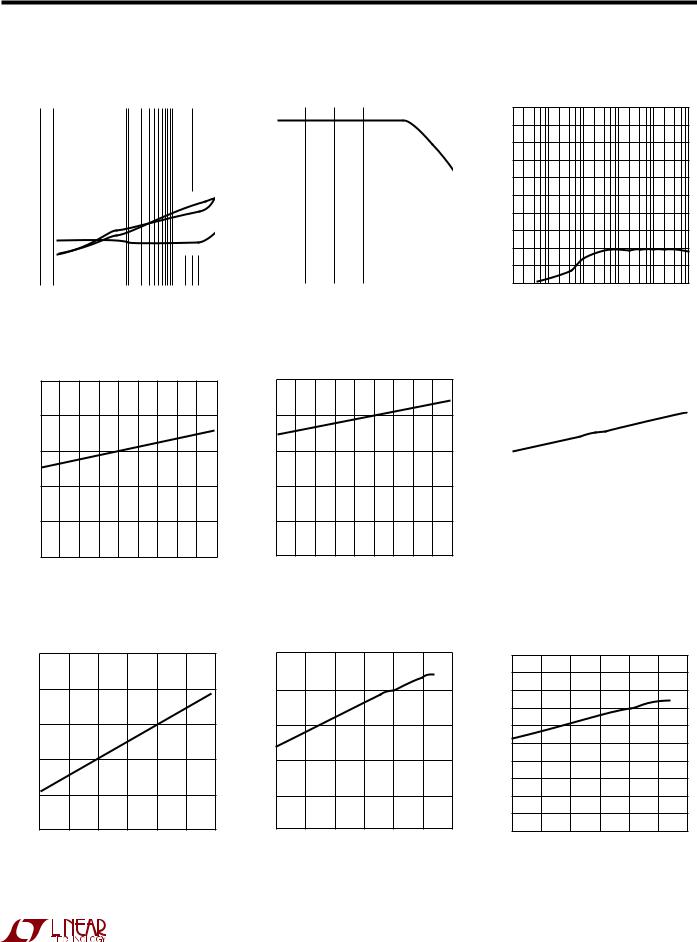
Power Supply Feedthrough |
|
|
|
|
|
|
|
|
|
|
|
Input Common Mode Rejection |
|
|
||||||||||||||||||||
|
|
vs Ripple Frequency |
|
|
|
|
|
|
|
|
|
|
|
|
|
vs Input Frequency |
|
|
|
|
|
|
||||||||||||||
|
0 |
|
|
|
|
|
|
|
|
|
|
|
|
|
|
|
|
|
|
|
|
|
|
|
|
|
90 |
|
|
|
|
|
|
|
|
|
|
–20 |
|
|
|
|
|
|
|
|
|
|
|
|
|
|
|
|
|
|
|
|
|
|
|
|
(dB) |
80 |
|
|
|
|
|
|
|
|
|
|
|
|
|
|
|
|
|
|
|
|
|
|
|
|
|
|
|
|
|
|
|
|
|
|
|
|
|
|
|
|
|
|
|
|||
|
|
|
|
|
|
|
|
|
|
|
|
|
|
|
|
|
|
|
|
|
|
|
|
|
70 |
|
|
|
|
|
|
|
|
|
||
|
|
|
|
|
|
|
|
|
|
|
|
|
|
|
|
|
|
|
|
|
|
|
|
|
|
|
|
|
|
|
|
|
|
|||
|
|
|
|
|
|
|
|
|
|
|
|
|
|
|
|
|
|
|
|
|
|
|
|
|
|
|
|
|
|
|
|
|
|
|
||
|
|
|
|
|
|
|
|
|
|
|
|
|
|
|
|
|
|
|
|
|
|
|
|
|
|
|
|
|
|
|
|
|
|
|
||
DISTORTION(dB) |
|
|
|
|
|
|
|
|
|
|
|
|
|
|
|
|
|
|
|
|
|
|
|
|
|
MODECOMMONREJECTION |
|
|
|
|
|
|
|
|
|
|
–100 |
|
|
|
|
|
|
|
|
|
|
|
|
|
|
|
|
DGND |
|
|
|
|
|
60 |
|
|
|
|
|
|
|
|
|
||||
|
–40 |
|
|
|
|
|
|
|
|
|
|
|
|
|
|
|
|
|
|
|
|
|
|
|
|
|
|
|
|
|
|
|
|
|
|
|
|
–60 |
|
|
|
|
|
|
|
|
|
|
|
|
|
|
|
|
|
|
|
|
|
|
|
|
|
50 |
|
|
|
|
|
|
|
|
|
|
|
|
|
|
|
|
|
|
|
|
|
|
|
|
|
VSS |
|
|
|
|
|
|
|
40 |
|
|
|
|
|
|
|
|
|
|||
|
|
|
|
|
|
|
|
|
|
|
|
|
|
|
|
|
|
|
|
|
|
|
|
|
|
|
|
|
|
|
|
|
|
|
|
|
|
–80 |
|
|
|
|
|
|
|
|
|
|
|
|
|
|
|
VDD |
|
|
|
|
|
|
|
30 |
|
|
|
|
|
|
|
|
|
||
|
|
|
|
|
|
|
|
|
|
|
|
|
|
|
|
|
|
|
|
|
|
|
|
|
|
|
|
|
|
|
|
|||||
|
|
|
|
|
|
|
|
|
|
|
|
|
|
|
|
|
|
|
|
|
|
|
|
|
|
|
20 |
|
|
|
|
|
|
|
|
|
|
|
|
|
|
|
|
|
|
|
|
|
|
|
|
|
|
|
|
|
|
|
|
|
|
|
|
|
|
|
|
|
|
|
|
|
|
|
|
|
|
|
|
|
|
|
|
|
|
|
|
|
|
|
|
|
|
|
|
|
|
|
|
|
|
|
|
|
|
|
|
|
|
|
|
|
|
|
|
|
|
|
|
|
|
|
|
|
|
|
|
|
|
|
|
|
|
|
|
|
|
10 |
|
|
|
|
|
|
|
|
|
|
|
|
|
|
|
|
|
|
|
|
|
|
|
|
|
|
|
|
|
|
|
|
|
|
|
|
|
|
|
|
|
|
|
|
|
|
|
–120 |
|
|
|
|
|
|
|
|
|
|
|
|
PERFORMANCE |
|
|
|
|
|
0 |
CHARACTERISTICS |
|
|
|
|
|
||||||||||
TYPICAL |
|
|
|
|
|
|
|
|
|
|
|
|
|
|
|
|
|
|
|
|||||||||||||||||
|
|
|
|
|
|
|
|
|
|
|
|
|
|
|
|
|
|
|
|
|
|
|
|
|
|
|
1 |
10 |
100 |
1k |
10k |
100k |
1M |
|||
|
1k |
10k |
|
|
|
|
100k |
1M |
|
|
|
|
|
|
|
10M |
|
|||||||||||||||||||
|
|
|
|
|
|
|
|
|
FREQUENCY (Hz) |
|
|
|
|
|
|
|
|
|
|
|
|
|
|
INPUT FREQUENCY (Hz) |
|
|
|
|
||||||||
|
|
|
|
|
|
|
|
|
|
|
|
|
|
|
|
|
|
|
1418 G10 |
|
|
|
|
|
|
|
|
1418 G11 |
||||||||
CHANGE IN OFFSET VOLTAGE (LSB)
Input Offset Voltage Shift vs Source Resistance
10
9 |
|
|
|
|
|
8 |
|
|
|
|
|
7 |
|
|
|
|
|
6 |
|
|
|
|
|
5 |
|
|
|
|
|
4 |
|
|
|
|
|
3 |
|
|
|
|
|
2 |
|
|
|
|
|
1 |
|
|
|
|
|
010 |
100 |
1k |
10k |
100k |
1M |
INPUT SOURCE RESISTANCE (Ω)
1418 G12
VDD Supply Current vs
Temperature (Unipolar Mode)
|
5 |
(mA) |
4 |
|
|
CURRENT |
3 |
SUPPLY |
2 |
|
|
DD |
1 |
V |
|
|
0 |
–75 –50 –25 0 25 50 75 100 125 150 TEMPERATURE (°C)
1418 G13
VDD Supply Current vs Sampling Frequency (Unipolar Mode)
|
5 |
(mA) |
4 |
|
|
CURRENT |
3 |
SUPPLY |
2 |
|
|
DD |
1 |
V |
|
|
0 |
0 50 100 150 200 250 300 SAMPLING FREQUENCY (kHz)
1418 G16
VDD Supply Current vs
Temperature (Bipolar Mode)
|
5 |
(mA) |
4 |
|
|
CURRENT |
3 |
SUPPLY |
2 |
|
|
DD |
1 |
V |
|
|
0 |
–75 –50 –25 0 25 50 75 100 125 150 TEMPERATURE (°C)
1418 G14
VDD Supply Current vs Sampling Frequency (Bipolar Mode)
|
5 |
(mA) |
4 |
|
|
CURRENT |
3 |
SUPPLY |
2 |
|
|
DD |
1 |
V |
|
|
0 |
0 50 100 150 200 250 300 SAMPLING FREQUENCY (kHz)
1418 G17
VSS Supply Current vs
Temperature (Bipolar Mode)
|
2.0 |
|
|
|
|
|
|
|
|
|
|
|
|
|
|
|
|
|
|
|
|
|
|
|
|
|
|
|
|
|
|
|
|
|
|
|
|
|
|
|
1.8 |
|
|
|
|
|
|
|
|
|
|
|
|
|
|
|
|
|
|
|
|
|
|
|
|
|
|
|
|
|
|
|
|
|
|
|
|
|
|
(mA) |
1.6 |
|
|
|
|
|
|
|
|
|
|
|
|
|
|
|
|
|
|
|
|
|
|
|
|
|
|
|
|
|
|
|
|
|
|
|
|
||
1.4 |
|
|
|
|
|
|
|
|
|
|
|
|
|
|
|
|
|
|
|
CURRENT |
|
|
|
|
|
|
|
|
|
|
|
|
|
|
|
|
|
|
|
1.0 |
|
|
|
|
|
|
|
|
|
|
|
|
|
|
|
|
|
|
|
SUPPLY |
1.2 |
|
|
|
|
|
|
|
|
|
|
|
|
|
|
|
|
|
|
0.6 |
|
|
|
|
|
|
|
|
|
|
|
|
|
|
|
|
|
|
|
SS |
0.8 |
|
|
|
|
|
|
|
|
|
|
|
|
|
|
|
|
|
|
|
|
|
|
|
|
|
|
|
|
|
|
|
|
|
|
|
|
||
0.4 |
|
|
|
|
|
|
|
|
|
|
|
|
|
|
|
|
|
|
|
|
|
|
|
|
|
|
|
|
|
|
|
|
|
|
|
|
|
||
V |
|
|
|
|
|
|
|
|
|
|
|
|
|
|
|
|
|
|
|
0.2 |
|
|
|
|
|
|
|
|
|
|
|
|
|
|
|
|
|
|
|
|
|
|
|
|
|
|
|
|
|
|
|
|
|
|
|
|
|
|
|
|
|
|
|
|
|
|
|
|
|
|
|
|
|
|
|
|
|
|
|
|
0 |
|
|
|
|
|
|
|
|
|
|
|
|
|
|
|
|
|
|
|
|
–50 |
|
|
0 |
25 |
50 |
|
|
100 |
125 |
150 |
|||||||
|
–75 |
–25 |
75 |
||||||||||||||||
TEMPERATURE (°C)
1418 G13
VSS Supply Current vs Sampling
Frequency (Bipolar Mode)
|
2.0 |
|
|
1.8 |
|
(mA) |
1.6 |
|
1.4 |
||
CURRENT |
||
1.0 |
||
SUPPLY |
1.2 |
|
0.6 |
||
|
0.8 |
|
SS |
0.4 |
|
V |
||
|
0.2 |
|
|
0 |
0 50 100 150 200 250 300 SAMPLING FREQUENCY (kHz)
1418 G18
|
|
1418fa |
|
|
|
|
|
|
|
For more information www.linear.com/LTC1418 |
7 |
|
||
|

LTC1418
PIN FUNCTIONS
AIN+ (Pin 1): Positive Analog Input.
AIN– (Pin 2): Negative Analog Input.
VREF (Pin 3): 2.50V Reference Output. Bypass to AGND with 1µF.
REFCOMP (Pin 4): 4.096V Reference Bypass Pin. Bypass to AGND with 10µF tantalum in parallel with 0.1µF ceramic.
AGND (Pin 5): Analog Ground.
D13 to D6 (Pins 6 to 13): Three-State Data Outputs (Parallel). D13 is the most significant bit.
DGND (Pin 14): Digital Ground for Internal Logic. Tie to AGND.
D5 (Pin 15): Three-State Data Output (Parallel).
D4 (EXTCLKIN) (Pin 16): Three-State Data Output (Parallel). Conversion clock input (serial) when Pin 20 (EXT/ INT) is tied high.
D3 (SCLK) (Pin 17): Three-State Data Output (Parallel). Data clock input (serial).
D2 (CLKOUT) (Pin 18): Three-State Data Output (Parallel). Conversion clock output (serial).
D1 (DOUT) (Pin 19): Three-State Data Output (Parallel). Serial data output (serial).
D0 (EXT/INT) (Pin 20): Three-State Data Output (Parallel). Conversion clock selector (serial). An input low enables the internal conversion clock. An input high indicates an external conversion clock will be assigned to Pin 16 (EXTCLKIN).
SER/PAR (Pin 21): Data Output Mode.
SHDN (Pin 22): Power Shutdown Input. Low selects shutdown. Shutdown mode selected by CS. CS = 0 for nap mode and CS = 1 for sleep mode.
RD (Pin 23): Read Input. This enables the output drivers when CS is low.
CONVST (Pin 24): Conversion Start Signal. This active low signal starts a conversion on its falling edge.
CS (Pin 25): Chip Select. This input must be low for the ADC to recognize the CONVST and RD inputs. CS also sets the shutdown mode when SHDN goes low. CS and SHDN low select the quick wake-up nap mode. CS high and SHDN low select sleep mode.
BUSY (Pin 26): The BUSY Output Shows the Converter Status. It is low when a conversion is in progress.
VSS (Pin 27): Negative Supply, –5V for Bipolar Operation. Bypass to AGND with 10µF tantalum in parallel with 0.1µF ceramic. Analog ground for unipolar operation.
VDD (Pin 28): 5V Positive Supply. Bypass to AGND with 10µF tantalum in parallel with 0.1µF ceramic.
TEST CIRCUITS |
|
|
|
|
|
|
|
|
|
|
|
|
|
|
|
|
|
|
|
Load Circuits for Output Float Delay |
|||||||||||||||||||||||||||||||||||||||
|
|
|
|
|
|
|
|
|
Load Circuits for Access Timing |
|
|
|
|
|
|
|
|||||||||||||||||||||||||||||||||||||||||||
|
|
|
|
|
|
|
|
|
|
|
|
|
|
|
|
|
|
|
|
|
|
|
|
|
|
|
|
|
|
|
|
|
|
|
|
|
|
||||||||||||||||||||||
|
|
|
|
|
|
|
|
|
|
|
|
|
|
|
|
|
|
|
|
|
|
5V |
|
|
|
|
|
|
|
|
|
|
|
|
|
|
|
|
|
|
|
|
|
5V |
|||||||||||||||
|
|
|
|
|
|
|
|
|
|
|
|
|
|
|
|
|
|
|
|
|
|
|
|
|
|
|
|
1k |
|
|
|
|
|
|
|
|
|
|
|
|
|
|
|
|
|
|
|
|
|
|
|
|
|
|
|
1k |
|||
|
|
|
|
|
|
|
|
|
|
|
|
|
|
|
|
|
|
|
|
|
|
|
|
|
|
|
|
|
|
|
|
|
|
|
|
|
|
|
|
|
|
|
|
|
|
|
|
|
|
|
|
|
|
|
|||||
DBN |
|
|
|
|
|
|
|
|
|
|
|
|
|
|
|
|
|
|
DBN |
|
|
|
|
|
|
|
|
|
|
|
DBN |
|
|
|
|
|
|
|
|
|
|
|
|
|
|
|
|
|
DBN |
|
|
|
|
|
|
|
|
|
|
|
|
|
|
|
|
|
|
1k |
|
|
|
|
|
|
|
|
|
CL |
|
|
|
|
|
|
|
|
|
|
CL |
|
|
|
|
|
|
|
|
1k |
|
|
|
|
|
30pF |
|
|
|
|
|
|
|
|
|
|
30pF |
||||
|
|
|
|
|
|
|
|
|
|
|
|
|
|
|
|
|
|
|
|
|
|
|
|
|
|
|
|
|
|
|
|
|
|
|
|
|
|
|
|
|
|
|
|
|
|
|
|
|
|
||||||||||
|
|
|
|
|
|
|
|
|
DGND |
|
|
|
|
|
|
|
|
|
|
|
|
|
|
|
|
|
DGND |
|
|
|
|
|
|
|
|
|
|
|
|
|
|
|
|
|
|
|
|
|
|
|
|
|
|
|
|
|
|||
|
|
|
|
|
|
|
|
|
|
|
|
|
|
|
|
|
|
|
|
|
|
|
|
|
|
|
|
|
|
|
|
|
|
|
|
|
|
|
|
|
|
|
|
|
|
|
|
|
|
|
|
|
|
|
|||||
A) HI-Z TO VOH AND VOL TO VOH |
B) HI-Z TO VOL AND VOH TO VOL |
|
|
|
|
|
A) VOH TO HI-Z |
|
|
|
|
|
|
B) VOL TO HI-Z |
|||||||||||||||||||||||||||||||||||||||||||||
|
|
|
|
|
|
|
|
|
|
|
|
|
|
|
|
|
|
|
|
|
|
|
|
|
|
|
|
|
1418 TC01 |
|
|
|
|
|
|
|
|
|
|
|
|
|
|
|
|
|
|
|
|
|
|
|
|
|
|
|
|
1418 TC02 |
|
|
|
|
|
|
|
|
|
|
|
|
|
|
|
|
|
|
|
|
|
|
|
|
|
|
|
|
|
|
|
|
|
|
|
|
|
|
|
|
|
|
|
|
|
|
|
|
|
|
|
|
|
|
|
|
|
|
|
||
|
|
|
1418fa |
|
|
||
|
|
|
|
8 |
For more information www.linear.com/LTC1418 |
|
|
|
|
||
|
|||