

MCP102/103/121/131
4.0APPLICATION INFORMATION
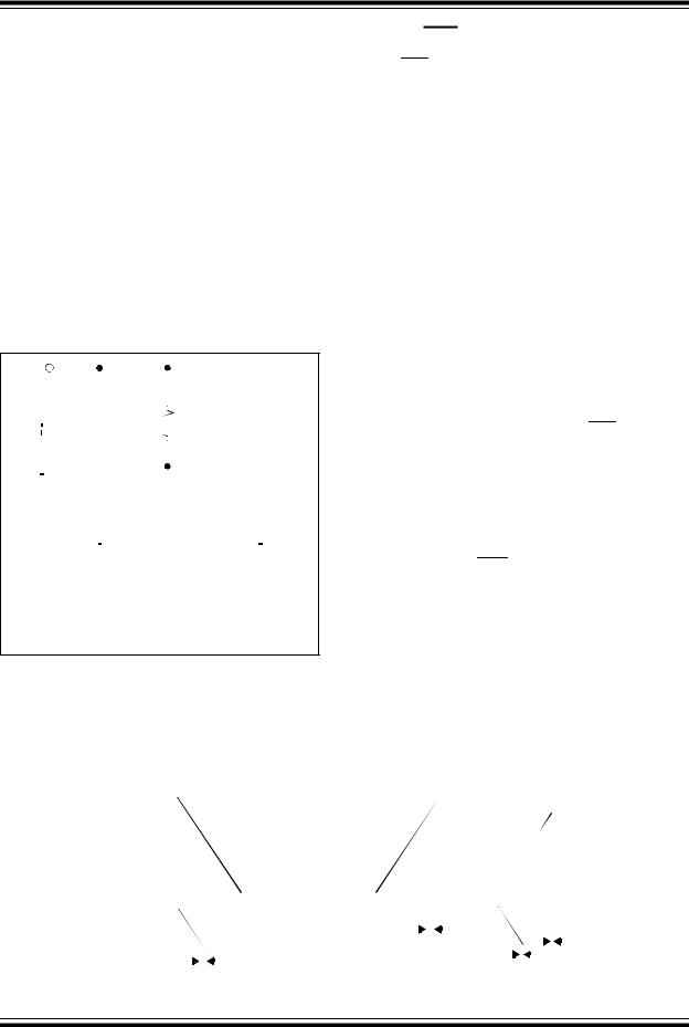
For many of today’s microcontroller applications, care must be taken to prevent low-power conditions that can cause many different system problems. The most common causes are brown-out conditions, where the system supply drops below the operating level momentarily. The second most common cause is when a slowly decaying power supply causes the microcontroller to begin executing instructions without sufficient voltage to sustain volitile memory (RAM), thus producing indeterminate results. Figure 4-1 shows a typical application circuit.
The MCP102/103/121/131 are voltage supervisor devices designed to keep a microcontroller in reset until the system voltage has reached and stabilized at the proper level for reliable system operation. These devices also operate as protection from brown-out conditions.
VDD |
|
|
|
|
|
|
|
|
|
|
|
|
|
|
|
|
|
|
|
|
|
|
|
|
|
|
|
|
|
|
|||||||
|
|
|
|
|
|
|
|
|
|
|
|
|
|
|
|
|
|
|
|
|
|
|
|
|
|
|
|
|
|
||||||||
|
|
|
|
|
|
|
|
|
|
|
|
|
|
|
|
|
|
|
|
|
|
|
|
|
|
|
|
|
VDD |
|
|||||||
0.1 |
|
|
|
|
|
|
|
|
|
|
VDD |
|
|
|
|
|
R |
PU |
|
|
PICmicro® |
|
|||||||||||||||
|
|
|
|
|
|
|
|
|
|
|
|
|
|
|
|
|
|
||||||||||||||||||||
|
|
|
|
|
|
|
|
MCP1XX |
|
|
|
|
|
|
|
|
|||||||||||||||||||||
µF |
|
|
|
|
|
|
|
|
|
|
|
|
|
|
|
|
Microcontroller |
|
|||||||||||||||||||
|
|
|
|
|
|
|
|
|
|
|
|
|
|
|
|
|
|||||||||||||||||||||
|
|
|
|
|
|
|
|
|
|
|
|
|
|
|
|
|
|
|
|
|
|
|
|
|
|
|
|
MCLR |
|
|
|
|
|
|
|||
|
|
|
|
|
|
|
|
|
|
|
|
|
|
|
|
|
RST |
|
|
|
|
|
|
|
|
|
(Reset input) |
|
|||||||||
|
|
|
|
|
|
|
|
|
|
|
|
|
|
|
|
|
|
|
|
|
|
|
|
|
|||||||||||||
|
|
|
|
|
|
|
|
|
|
VSS |
|
|
|
|
|
|
|
|
(Active-low) |
|
|||||||||||||||||
|
|
|
|
|
|
|
|
|
|
|
|
|
|
|
|
|
|
|
VSS |
|
|||||||||||||||||
|
|
|
|
|
|
|
|
|
|
|
|
|
|
|
|
|
|
|
|
|
|
|
|
|
|
|
|
|
|
||||||||
|
|
|
|
|
|
|
|
|
|
|
|
|
|
|
|
|
|
|
|
|
|
|
|
|
|
|
|
|
|
|
|
|
|
|
|
|
|
|
|
|
|
|
|
|
|
|
|
|
|
|
|
|
|
|
|
|
|
|
|
|
|
|
|
|
|
|
|
|
|
|
|
|
|
|
|
|
|
|
|
|
|
|
|
|
|
|
|
|
|
|
|
|
|
|
|
|
|
|
|
|
|
|
|
|
|
|
|
|
|
|
|
|
|
Note 1: Resistor RPU may be required with the MCP121 due to the open-drain output. Resistor RPU may not be required with the MCP131 due to the internal pull-up resistor. The MCP102 and MCP103 do not require the external pull-up resistor.
FIGURE 4-1: Typical Application Circuit.
4.1RST Operation
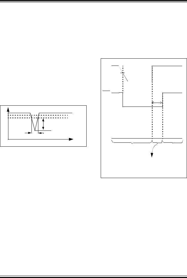
The RST output pin operation determines how the device can be used and indicates when the system should be forced into reset. To accomplish this, an internal voltage reference is used to set the voltage trip point (VTRIP). Additionally, there is a hysteresis on this trip point.
When the falling edge of VDD crosses this voltage threshold, the reset power-down timer (TRPD) starts. When this delay timer times out, the RST pin is forced low.
When the rising-edge of VDD crosses this voltage threshold, the reset power-up timer (TRPU) starts. When this delay timer times out, the RST pin is forced high, TRPU is active and there is additional system current.
The actual voltage trip point (VTRIPAC) will be between the minimum trip point (VTRIPMIN) and the maximum trip point (VTRIPMAX). The hysteresis on this trip point and the delay timer (TRPU) are to remove any “jitter”
that would occur on the RST pin when the device VDD is at the trip point.
Figure 4-2 shows the waveform of the RST pin as determined by the VDD voltage, while Table 4-1 shows the
state of the RST pin. The VTRIP specification is for falling VDD voltages. When the VDD voltage is rising, the RST
will not be driven high until VDD is at VTRIP + VHYS. Once VDD has crossed the voltage trip point, there is also a
minimal delay time (TRPD) before the RST pin is driven low.
TABLE 4-1: RST PIN STATES
|
|
|
|
|
|
|
State of RST Pin when: |
|
|||
|
|
|
|
|
|
Device |
VDD < VTRIP |
VDD > |
Ouput Driver |
||
|
|
|
VTRIP + VHYS |
|
|
|
|
|
|
|
|
MCP102 |
L |
|
H |
Push-pull |
|
|
|
|
|
|
|
MCP103 |
L |
|
H |
Push-pull |
|
|
|
|
|
|
|
MCP121 |
L |
|
H (1) |
Open-drain (1) |
|
MCP131 |
L |
|
H (2) |
Open-drain (2) |
|
Note 1: Requires External Pull-up resistor
2: Has Internal Pull-up resistor
|
VDD |
|
|
|
|
|
|
|
|
|
|
|
|
|
|
|
|
|
|
|
|
|
|
VTRIPAC + VHYSAC |
|
|
|
|
|
|
|
|
|
|
|
|
|
|
|
|
|
|
|
|
|
|
|
|
|
|
|
|
|
|
|
|
||||||||||||||||
|
VTRIPMAX |
|
|
|
|
|
|
|
|
|
|
|
|
|
|
|
|
|
|
|
|
|
|
|
|
|
|
|
|
|
|
|
|
|
|
|
|
|
|
|
|
|
|
|
|
|
|
|
|
|||||||||||||||||||||||
|
|
|
|
|
|
|
|
|
|
|
|
|
|
|
|
|
|
|
|
|
|
|
|
|
|
|
|
|
|
|
|
|
|
|
|
|
|
|
|
|
|
|
|
|
|
VTRIPAC |
||||||||||||||||||||||||||
|
|
|
|
|
|
|
|
|
|
|
|
|
|
|
|
|
|
|
|
|
|
|
|
|
|
|
|
|
|
|
|
|
|
|
|
|
|
|||||||||||||||||||||||||||||||||||
|
|
|
|
|
|
|
|
|
|
|
|
|
|
|
|
|
|
|
|
|
|
|
|
|
|
|
|
|
|
|
|
|
|
|
|
|
|
|
|
|
|
|
|
|
|
|
|
|
|
|
|
|
|
|
|
|
|
|
|
|
|
|
|
|
|
|
|
|
||||
|
|
|
|
VTRIPMIN |
|
|
|
|
|
|
|
|
|
|
|
|
|
|
|
|
|
|
|
|
|
|
|
|
|
|
|
|
|
|
|
|
|
VTRIPAC |
|
|
|
|||||||||||||||||||||||||||||||
|
|
|
|
|
1V |
|
|
|
|
|
|
|
|
|
|
|
|
|
|
|
|
|
|
|
|
|
|
|
|
|
|
|
|
|
|
|
|
|
|
|
|
|
|
|
|
|||||||||||||||||||||||||||
|
|
|
|
|
|
|
|
|
|
|
|
|
|
|
|
|
|
|
|
|
|
|
|
|
|
|
|
|
|
|
|
|
|
|
|
|
|
|
|
|
|
|
|
|
|
|
|
|
|
|
|
|
|
|
|
|
|
|
|
|
|
|
|
|
|
|
|
|
||||
|
|
|
|
|
|
|
|
|
|
|
|
|
|
|
|
|
|
|
|
|
|
|
|
|
|
|
|
|
|
|
|
|
|
|
|
|
|
|
|
|
|
|
|
|
|
|
|
|
|
|
|
|
|
|
|
|
|
|
|
|
|
|||||||||||
|
|
|
|
|
|
|
|
|
|
|
|
|
|
|
|
|
|
|
|
|
|
|
|
|
|
|
|
|
|
|
|
|
|
|
|
|
|
|
|
|
|
|
|
|
|
|
|
|
|
|
|
|
|
|
|
|
|
|
|
|
|
|
|
|
|
|
|
|
||||
|
|
|
|
|
|
|
|
|
|
|
|
|
|
|
|
|
|
|
|
|
|
|
|
|
|
|
|
|
|
|
|
|
|
|
|
|
|
|
|
|
|
|
|
|
|
|
|
|
|
|
|
|
|
|
|
|
|
|
|
|
|
|||||||||||
|
|
|
|
|
|
|
|
|
|
|
|
|
|
|
|
|
|
|
|
|
|
|
|
|
|
|
|
|
|
|
|
|
|
|
|
|
|
|
|
|
|
|
|
|
|
|
|
|
|
|
|
|
|
|
|
|
|
|
|
|
|
|||||||||||
|
|
|
|
|
|
|
|
|
|
|
|
|
|
|
|
|
|
|
|
|
|
|
|
|
|
|
|
|
|
|
|
|
|
|
|
|
|
|
|
|
|
|
|
|
|
|
|
|
|
|
|
|
|
|
|
|
|
|
|
|
|
|||||||||||
|
|
|
|
|
|
|
|
|
|
|
|
|
|
|
|
|
|
|
|
|
|
|
|
|
|
|
|
|
|
|
|
|
|
|
|
|
|
|
|
|
|
|
|
|
|
|
|
|
|
|
|
|
|
|
|
|
|
|
|
|
|
|
|
|
|
|
|
|
|
|
|
|
|
|
|
|
|
|
|
|
|
|
|
|
|
|
|
|
|
|
|
|
|
|
|
|
|
|
|
|
|
|
|
|
|
|
|
|
|
|
|
|
|
|
|
|
|
|
|
|
|
|
|
|
|
|
|
|
|
|
|
|
|
|
|
|
|
|
|
|
|
|
|
|
|
|
RST |
|
|
|
|
|
|
|
|
|
|
|
|
|
|
|
|
|
|
|
|
|
|
|
|
|
|
|
|
|
|
|
|
|
|
|
|
|
|
|
|
|
|
|
|
|
tRPU |
|
|
|
|
|
|
|
|
tRPU |
||||||||||||||||
|
|
|
|
tRPD |
|
|
|
|
|
|
|
|
|
|
< 1V is outside the |
|
|
|
|
|
|
|
|
|
|
|
tRPD |
|
|
|
|
|
|
|
|
|
|
|
|
|
|
|
|
|||||||||||||||||||||||||||||
|
|
|
|
|
|
|
|
|
|
|
|
|
|
|
|
|
|
|
|
|
|
|
|
|
|
|
|
|
|
|
|
|
|
|
|
|||||||||||||||||||||||||||||||||||||
|
|
|
|
|
|
|
|
|
|
|
|
|
|
device specifications |
|
|
|
|
|
|
|
|
|
|
|
|
|
|
|
|
|
|
|
|
|
|
|
|
|
|
|
|
|
|
|
|
|
|
||||||||||||||||||||||||
|
|
|
|
|
|
|
|
|
|
|
|
|
|
|
|
|
|
|
|
|
|
|
|
|
|
|
|
|
|
|
|
|
|
|
|
|
|
|
|
|
|
|
|
|
|
|
|
|
|
|
|
|
|
|
|
|
|
|
|
|
|
|
|
|
|
|
|
|
|
|
|
|
|
|
|
|
|
|
|
|
|
|
|
|
|
|
|
|
|
|
|
|
|
|
|
|
|
|
|
|
|
|
|
|
|
|
|
|
|
|
|
|
|
|
|
|
|
|
|
|
|
|
|
|
|
|
|
|
|
|
|
|
|
|
|
|
|
|
|
|
|
|
|
|
|
FIGURE 4-2: RST Operation as Determined by the VTRIP and VHYS.
DS21906B-page 12 |
♥ 2005 Microchip Technology Inc. |
MCP102/103/121/131
4.2Negative Going VDD Transients
The minimum pulse width (time) required to cause a reset may be an important criteria in the implementation of a Power-on Reset (POR) circuit. This time is referred to as transient duration, defined as the amount of time needed for these supervisory devices to respond to a drop in VDD. The transient duration time is
dependant on the magnitude of VTRIP – VDD. Generally speaking, the transient duration decreases with
increases in VTRIP – VDD.
Figure 4-3 shows a typical transient duration vs. reset comparator overdrive, for which the MCP102/103/121/131 will not generate a reset pulse. It shows that the farther below the trip point the transient pulse goes, the duration of the pulse required to cause a reset gets shorter. Figure 2-32 shows the transient response characteristics for the MCP102/103/121/131.
A 0.1 µF bypass capacitor, mounted as close as possible to the VDD pin, provides additional transient immunity (refer to Figure 4-1).
5V |
VTRIP(MAX) |
|
Voltage |
||
VTRIP(MIN) |
||
VTRIP(MIN) - VDD |
||
Supply |
tTRANS |
|
0V |
Time (µs) |
FIGURE 4-3: Example of Typical
Transient Duration Waveform.
4.3Reset Power-up Timer (tRPU)
Figure 4-4 illustrates the device current states. While the system is powering down, the device has a low current. This current is dependent on the device VDD and trip point. When the device VDD rises through the voltage trip point (VTRIP), an internal timer starts. This timer consumes additional current until the RST pin is driven (or released) high. This time is known as the Reset Power-up Time (tRPU). Figure 4-4 shows when tRPU is active (device consuming additional current).
VDD |
|
|
|
|
VTRIP |
|
|
|
|
RST |
tRPU |
|
||
|
|
|||
|
Power-up |
Active |
Reset |
|
|
Power-up |
|||
Reset Power-up |
Reset |
Timer |
||
Timer |
||||
Timer Inactive |
Inactive |
|||
See Figures 2-1, |
|
See Figures 2-1, |
||
2-2 and 2-3 |
|
|
2-2 and 2-3 |
|
See Figures 2-4, |
||||
2-5 and |
2-6 |
|
||
FIGURE 4-4: Reset Power-up Timer
Waveform.
4.3.1EFFECT OF TEMPERATURE ON RESET POWER-UP TIMER (TRPU)
The Reset Power-up timer time-out period (tRPU) determines how long the device remains in the reset
condition. This is affected by both VDD and temperature. Typical responses for different VDD values and temperatures are shown in Figures 2-26, 2-27 and 2-28.
♥ 2005 Microchip Technology Inc. |
DS21906B-page 13 |
MCP102/103/121/131
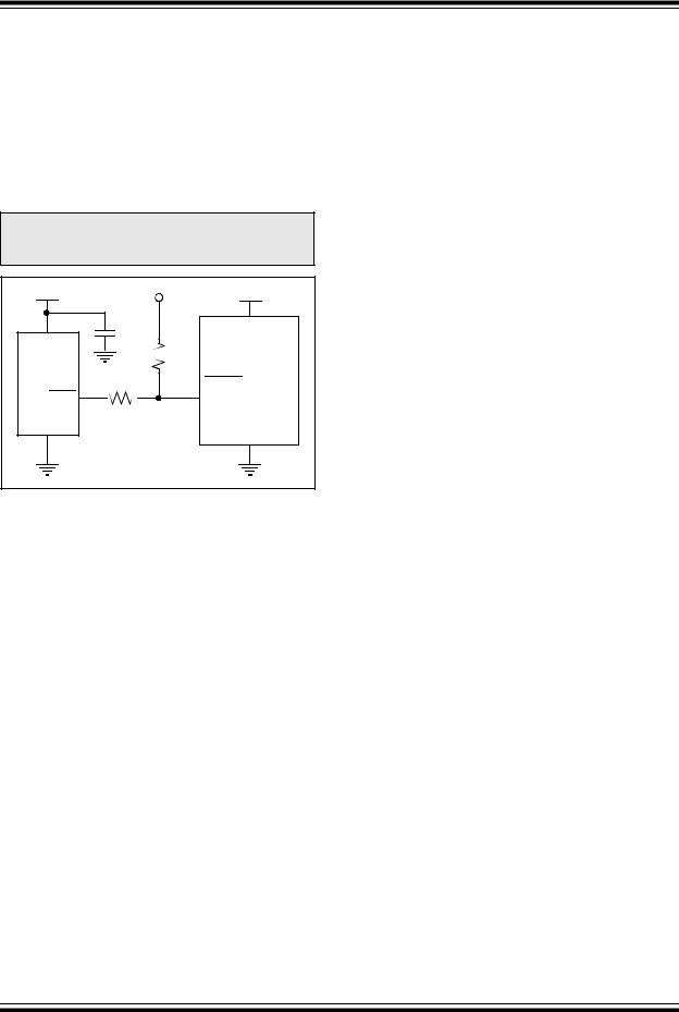
4.4Using in PICmicro® Microcontroller, ICSP™ Applications (MCP121 only)
Figure 4-5 shows the typical application circuit for using the MCP121 for voltage superviory function when the PICmicro microcontroller will be programmed via the ICSP feature. Additional information is available in TB087, “Using Voltage Supervisors with PICmicro® Microcontroller Systems which Implement In-Circuit Serial Programming™”, DS91087.
Note: It is recommended that the current into the RST pin be current limited by a 1 kΩ resistor.
|
VDD/VPP |
0.1µF |
VDD |
|
|
VDD |
RPU |
PICmicro® |
|
MCP121 |
MCU |
RST |
MCLR |
(Reset Input) |
|
1 kΩ |
(Active-low) |
VSS |
VSS |
|
FIGURE 4-5: Typical Application Circuit for PICmicro® Microcontroller with the ICSP™ feature.
DS21906B-page 14 |
♥ 2005 Microchip Technology Inc. |