

datasheet
.pdfDESCRIPTION
The TDA2030 is a monolithic integrated circuit in Pentawatt package, intended for use as a low frequency class AB amplifier. Typically it provides 14W output power (d = 0.5%) at 14V/4Ω; at ± 14V the guaranteed output power is 12W on a 4Ω load and 8W on a 8Ω (DIN45500).
The TDA2030provideshigh outputcurrent and has very low harmonic and cross-over distortion. Further the device incorporates an original (and patented) short circuit protection system comprising an arrangement for automatically limiting the dissipated power so as to keep the working point of the output transistors within their safe operating area. A conventional thermal shut-down system is also included.
ABSOLUTE MAXIMUM RATINGS
Symbol |
Parameter |
Vs |
Supply voltage |
Vi |
Input voltage |
Vi |
Differential input voltage |
Io |
Output peak current (internally limited) |
Ptot |
Power dissipation at Tcase = 90°C |
Tstg, Tj |
Stoprage and junction temperature |
TYPICAL APPLICATION
TDA2030
14W Hi-Fi AUDIO AMPLIFIER
Pentawatt
ORDERING NUMBERS : TDA2030H
TDA2030V
Value |
Unit |
± 18 |
V |
Vs |
|
± 15 |
V |
3.5 |
A |
20 |
W |
-40 to 150 |
°C |
March 1993 |
1/11 |

TDA2030
PIN CONNECTION (top view)
+VS OUTPUT -VS
INVERTING INPUT NON INVERTING INPUT
TEST CIRCUIT
2/11

|
|
|
|
TDA2030 |
THERMAL DATA |
|
|
|
|
Symbol |
Parameter |
|
Value |
Unit |
Rth j-case |
Thermal resistance junction-case |
max |
3 |
°C/W |
ELECTRICAL CHARACTERISTICS (Refer to the test circuit, Vs = ± 14V, Tamb = 25°C unless otherwise specified)
Symbol |
Parameter |
Vs |
Supply voltage |
Id |
Quiescent drain current |
Ib |
Input bias current |
Vos |
Input offset voltage |
Ios |
Input offset current |
Po |
Output power |
d Distortion
BPower Bandwidth (-3 dB)
Ri |
Input resistance (pin 1) |
Gv |
Voltage gain (open loop) |
Gv |
Voltage gain (closed loop) |
eN |
Input noise voltage |
iN |
Input noise current |
SVR |
Supply voltage rejection |
Id |
Drain current |
Tj |
Thermal shut-down junction |
|
temperature |
Test conditions |
Min. |
Typ. |
Max. |
Unit |
|
|
|
± 6 |
|
± 18 |
V |
|
|
|
40 |
60 |
mA |
|
|
|
0.2 |
2 |
μA |
Vs = ± 18V |
|
|
± 2 |
± 20 |
mV |
|
|
|
|||
|
|
|
± 20 |
± 200 |
nA |
d = 0.5% |
Gv = 30 dB |
|
|
|
|
f = 40 to 15,000 Hz |
|
|
|
|
|
RL = 4Ω |
|
12 |
14 |
|
W |
RL = 8Ω |
|
8 |
9 |
|
W |
d = 10% |
Gv = 30 dB |
|
|
|
|
f = 1 KHz |
|
|
|
|
|
RL = 4Ω |
|
|
18 |
|
W |
RL = 8Ω |
|
|
11 |
|
W |
Po = 0.1 to 12W |
|
|
|
|
|
RL = 4Ω |
Gv = 30 dB |
|
0.2 |
0.5 |
% |
f = 40 to 15,000 Hz |
|
||||
Po = 0.1 to 8W |
|
|
|
|
|
RL = 8Ω |
Gv = 30 dB |
|
0.1 |
0.5 |
% |
f = 40 to 15,000 Hz |
|
||||
Gv = 30 dB |
|
|
10 to 140,000 |
|
Hz |
Po = 12W |
RL = 4Ω |
|
|
||
|
|
|
|
||
|
|
0.5 |
5 |
|
MΩ |
|
|
|
90 |
|
dB |
|
f = 1 kHz |
29.5 |
30 |
30.5 |
dB |
B = 22 Hz to 22 KHz |
|
3 |
10 |
μV |
|
|
|
|
80 |
200 |
pA |
RL = 4Ω |
Gv = 30 dB |
40 |
50 |
|
dB |
Rg = 22 kΩ |
|
|
|
|
|
Vripple = 0.5 Veff |
|
|
|
|
|
fripple = 100 Hz |
|
|
|
|
|
Po = 14W |
RL = 4Ω |
|
900 |
|
mA |
Po = W |
RL = 8Ω |
|
500 |
|
mA |
|
|
|
145 |
|
°C |
3/11
TDA2030
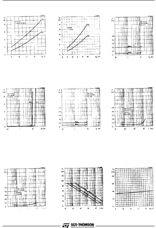
Figure 1. Output power vs. supply voltage
Fi gur e 4. Di stortion v s. output power
F igu r e 7. Di stor ti on vs . frequency
Figure 2. Output power vs. supply voltage
F ig ure 5. Di stortion vs. output power
Fig ure 8. Fre que nc y re - sponse with different values of the rolloff capacitor C8 (see fig. 13)
F ig u re 3 . Di stor ti on v s. output power
F ig u re 6 . Di stor ti on v s. frequency
Figure 9. Quiescent current vs. supply voltage
4/11

Figure 10. Supply voltage |
Figure 11. Power dissipa- |
rejection vs. voltage gain |
tion and efficiency vs. output |
|
power |
TDA2030
Figure 12. Maximum power dissipation vs. supply voltage (sine wave operation)
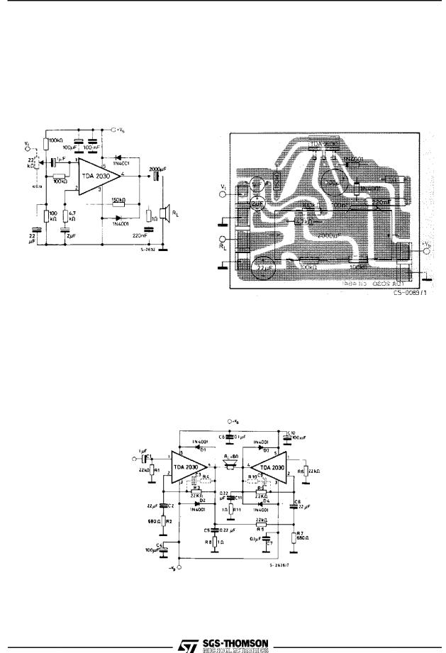
APPLICATION INFORMATION |
|
Figure 13. Typical amplifier |
Figure 14. P.C. board and component layout for |
with split power supply |
the circuit of fig. 13 (1 : 1 scale) |
5/11
TDA2030
APPLICATION INFORMATION (continued)
Figure 15. Typical amplifier |
Figure 16. P.C. board and component layout for |
with single power supply |
the circuit of fig. 15 (1 : 1 scale) |
Figure 17. Bridge amplifier configuration with split power supply (Po = 28W, Vs = ±14V)
6/11

TDA2030
PRACTICAL CONSIDERATIONS
Printed circuit board
The layout shown in Fig. 16 should be adopted by the designers. If different layouts are used, the ground points of input 1 and input 2 must be well decoupled from the ground return of the output in which a high current flows.
Assembly suggestion
No electrical isolation is needed between the
Component |
Recomm. |
Purpose |
|
|
value |
||
|
|
|
|
R1 |
|
22 kΩ |
Closed loop gain |
|
|
|
setting |
R2 |
|
680 Ω |
Closed loop gain |
|
|
|
setting |
R3 |
|
22 kΩ |
Non inverting input |
|
|
|
biasing |
R4 |
|
1 Ω |
Frequency stability |
R5 |
|
3 R2 |
Upper frequency |
|
|
|
cutoff |
C1 |
|
1 μF |
Input DC |
|
|
|
decoupling |
C2 |
|
22 μF |
Inverting DC |
|
|
|
decoupling |
C3, C4 |
|
0.1 μF |
Supply voltage |
|
|
|
bypass |
C5, C6 |
|
100 μF |
Supply voltage |
|
|
|
bypass |
C7 |
|
0.22 μF |
Frequency stability |
C8 |
|
1 |
Upper frequency |
|
2π B R1 |
cutoff |
|
packageand the heatsinkwith singlesupplyvoltage configuration.
Application suggestions
The recommended values of the components are those shown on application circuit of fig. 13. Different values can be used. The following table can help the designer.
Larger than |
Smaller than |
recommended value |
recommended value |
Increase of gain |
Decrease of gain (*) |
Decrease of gain (*) |
Increase of gain |
Increase of input |
Decrease of input |
impedance |
impedance |
Danger of osccilat. at |
|
high frequencies |
|
with induct. loads |
|
Poor high frequencies |
Danger of |
attenuation |
oscillation |
|
Increase of low |
|
frequencies cutoff |
|
Increase of low |
|
frequencies cutoff |
|
Danger of |
|
oscillation |
|
Danger of |
|
oscillation |
|
Danger of oscillation |
Smaller bandwidth |
Larger bandwidth |
D1, D2 |
1N4001 |
To protect the device against output voltage spikes |
(*) Closed loop gain must be higher than 24dB
7/11

TDA2030
SHORT CIRCUIT PROTECTION
The TDA2030 has an original circuit which limits the current of the output transistors. Fig. 18 shows that the maximum output current is a function of the collector emitter voltage; hence the output transistors work within their safe operating area (Fig. 2). This function can therefore be considered as being
F i gu r e 1 8. Ma ximum o u tpu t c urr en t v s . voltage [VCEsat] across each output transistor
THERMAL SHUT-DOWN
The presence of a thermal limiting circuit offers the following advantages:
1.An overload on the output (even if it is permanent), or an abovelimit ambient temperaturecan
be easily supported since the Tj cannot be higher than 150°C.
2.The heatsink can have a smaller factor of safety compared with that of a conventional circuit. There is no possibility of device damage due to high junction temperature.If for any reason, the
peak power limiting rather than simple current limiting.
It reduces the possibility that the device gets damaged during an accidental short circuit from AC output to ground.
Figure 19. Safe operating area and collector characteristics of the protected power transistor
junction temperature increases up to 150°C, the thermal shut-down simply reduces the power dissipation at the current consumption.
The maximum allowable power dissipation depends upon the size of the external heatsink (i.e. its thermal resistance); fig. 22 shows this dissipable power as a function of ambient temperature for different thermal resistance.
8/11
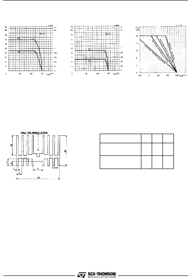
Figure 20. Output power and d ra i n cu r ren t vs. c ase
temperature (RL = 4Ω)
Figure 21. Output power and d r a i n c u rr en t vs. c as e
temperature (RL = 8Ω)
TDA2030
F i gu r e 2 2. Ma ximum allowable power dissipation vs. ambient temperature
Figure 23. Example of heat-sink |
Dimension : suggestion. |
|
|
|
|
The following table shows the length that |
|||||
|
|||||
|
the heatsink in fig.23 must have for several |
||||
|
values of Ptot and Rth. |
|
|
|
|
|
Ptot (W) |
12 |
8 |
6 |
|
|
Length of heatsink |
60 |
40 |
30 |
|
|
(mm) |
||||
|
|
|
|
||
|
Rth of heatsink |
4.2 |
6.2 |
8.3 |
|
|
(° C/W) |
||||
|
|
|
|
||
9/11
TDA2030
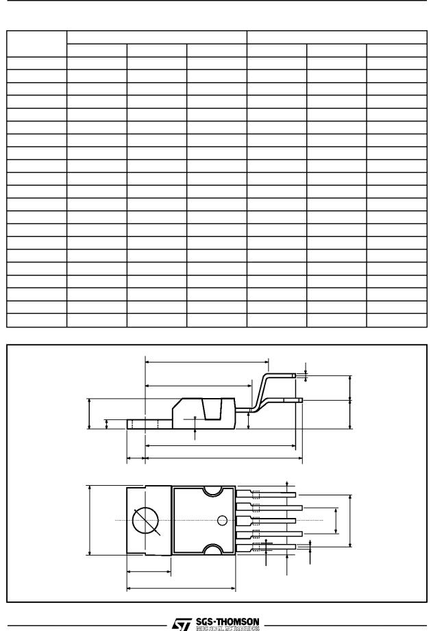
PENTAWATT PACKAGE MECHANICAL DATA
DIM. |
|
mm |
|
|
inch |
|
|
MIN. |
TYP. |
MAX. |
MIN. |
TYP. |
MAX. |
||
|
|||||||
A |
|
|
4.8 |
|
|
0.189 |
|
C |
|
|
1.37 |
|
|
0.054 |
|
D |
2.4 |
|
2.8 |
0.094 |
|
0.110 |
|
D1 |
1.2 |
|
1.35 |
0.047 |
|
0.053 |
|
E |
0.35 |
|
0.55 |
0.014 |
|
0.022 |
|
F |
0.8 |
|
1.05 |
0.031 |
|
0.041 |
|
F1 |
1 |
|
1.4 |
0.039 |
|
0.055 |
|
G |
|
3.4 |
|
0.126 |
0.134 |
0.142 |
|
G1 |
|
6.8 |
|
0.260 |
0.268 |
0.276 |
|
H2 |
|
|
10.4 |
|
|
0.409 |
|
H3 |
10.05 |
|
10.4 |
0.396 |
|
0.409 |
|
L |
|
17.85 |
|
|
0.703 |
|
|
L1 |
|
15.75 |
|
|
0.620 |
|
|
L2 |
|
21.4 |
|
|
0.843 |
|
|
L3 |
|
22.5 |
|
|
0.886 |
|
|
L5 |
2.6 |
|
3 |
0.102 |
|
0.118 |
|
L6 |
15.1 |
|
15.8 |
0.594 |
|
0.622 |
|
L7 |
6 |
|
6.6 |
0.236 |
|
0.260 |
|
M |
|
4.5 |
|
|
0.177 |
|
|
M1 |
|
4 |
|
|
0.157 |
|
|
Dia |
3.65 |
|
3.85 |
0.144 |
|
0.152 |
|
|
|
|
L |
|
|
|
|
|
|
|
|
|
E |
|
|
|
|
|
L1 |
|
M1 |
|
|
|
|
|
|
|
|
||
A |
C |
|
|
D |
M |
|
|
|
|
|
D1 |
|
|
|
|
|
|
|
L2 |
|
|
|
|
|
|
L5 |
L3 |
|
|
|
H3 |
|
|
G |
G1 |
Dia. |
|
|
|
|
L7 |
F1 |
H2 |
F |
|
|
|
|
|
|
|
L6 |
|
|
|
10/11