

- •1 Central processing unit (CPU)
- •1.1 Introduction
- •1.2 CPU registers
- •1.2.1 Description of CPU registers
- •Figure 2. Stacking order
- •1.2.2 STM8 CPU register map
- •1.3 Global configuration register (CFG_GCR)
- •1.3.1 Activation level
- •1.3.2 SWIM disable
- •1.3.3 Description of global configuration register (CFG_GCR)
- •1.3.4 Global configuration register map and reset values
- •Table 3. CFG_GCR register map
- •2 Boot ROM
- •3 Memory and register map
- •3.1 Memory layout
- •3.1.1 Memory map
- •Figure 3. Memory map
- •3.1.2 Stack handling
- •Figure 4. Default stack model
- •Figure 5. Customized stack model
- •3.2 Register description abbreviations
- •4 Flash program memory and data EEPROM
- •4.1 Introduction
- •4.2 Glossary
- •4.3 Main Flash memory features
- •4.4 Memory organization
- •4.4.1 STM8S and STM8AF memory organization
- •Figure 6. Flash memory and data EEPROM organization on low density STM8S and STM8AF
- •Figure 7. Flash memory and data EEPROM organization on medium density STM8S and STM8AF
- •Figure 8. Flash memory and data EEPROM organization high density STM8S and STM8AF
- •4.4.2 Memory access/ wait state configuration
- •4.4.3 User boot area (UBC)
- •Figure 9. UBC area size definition on low density STM8S devices
- •4.4.4 Data EEPROM (DATA)
- •4.4.5 Main program area
- •4.4.6 Option bytes
- •4.5 Memory protection
- •4.5.1 Readout protection
- •4.5.2 Memory access security system (MASS)
- •4.5.3 Enabling write access to option bytes
- •4.6 Memory programming
- •4.6.2 Byte programming
- •4.6.3 Word programming
- •4.6.4 Block programming
- •4.6.5 Option byte programming
- •4.8 Flash registers
- •4.8.1 Flash control register 1 (FLASH_CR1)
- •4.8.2 Flash control register 2 (FLASH_CR2)
- •4.8.3 Flash complementary control register 2 (FLASH_NCR2)
- •4.8.4 Flash protection register (FLASH_FPR)
- •4.8.5 Flash protection register (FLASH_NFPR)
- •4.8.6 Flash program memory unprotecting key register (FLASH_PUKR)
- •4.8.7 Data EEPROM unprotection key register (FLASH_DUKR)
- •4.8.8 Flash status register (FLASH_IAPSR)
- •4.8.9 Flash register map and reset values
- •5 Single wire interface module (SWIM) and debug module (DM)
- •5.1 Introduction
- •5.2 Main features
- •Figure 12. SWIM pin connection
- •5.3 SWIM modes
- •6 Interrupt controller (ITC)
- •6.1 ITC introduction
- •6.2 Interrupt masking and processing flow
- •Figure 13. Interrupt processing flowchart
- •6.2.1 Servicing pending interrupts
- •Figure 14. Priority decision process
- •6.2.2 Interrupt sources
- •6.3 Interrupts and low power modes
- •6.4 Activation level/low power mode control
- •6.5 Concurrent and nested interrupt management
- •6.5.1 Concurrent interrupt management mode
- •Figure 15. Concurrent interrupt management
- •6.5.2 Nested interrupt management mode
- •Table 10. Vector address map versus software priority bits
- •Figure 16. Nested interrupt management
- •6.6 External interrupts
- •6.7 Interrupt instructions
- •6.8 Interrupt mapping
- •6.9 ITC and EXTI registers
- •6.9.1 CPU condition code register interrupt bits (CCR)
- •6.9.2 Software priority register x (ITC_SPRx)
- •6.9.3 External interrupt control register 1 (EXTI_CR1)
- •6.9.4 External interrupt control register 1 (EXTI_CR2)
- •6.9.5 ITC and EXTI register map and reset values
- •7 Power supply
- •Figure 17. Power supply overview
- •8 Reset (RST)
- •Figure 18. Reset circuit
- •8.1 “Reset state” and “under reset” definitions
- •8.2 Reset circuit description
- •8.3 Internal reset sources
- •Figure 19. VDD/VDDIO voltage detection: POR/BOR threshold
- •8.3.2 Watchdog reset
- •8.3.3 Software reset
- •8.3.4 SWIM reset
- •8.3.5 Illegal opcode reset
- •8.3.6 EMC reset
- •8.4 RST register description
- •8.4.1 Reset status register (RST_SR)
- •8.5 RST register map
- •Table 13. RST register map
- •9 Clock control (CLK)
- •9.1 Master clock sources
- •Figure 21. HSE clock sources
- •Table 14. Devices with 4 trimming bits
- •Table 15. Devices with 3 trimming bits
- •9.2 Master clock switching
- •9.2.1 System startup
- •9.2.2 Master clock switching procedures
- •Figure 22. Clock switching flowchart (automatic mode example)
- •Figure 23. Clock switching flowchart (manual mode example)
- •9.3 Low speed clock selection
- •9.4 CPU clock divider
- •9.5 Peripheral clock gating (PCG)
- •9.6 Clock security system (CSS)
- •9.8 CLK interrupts
- •Table 16. CLK interrupt requests
- •9.9 CLK register description
- •9.9.1 Internal clock register (CLK_ICKR)
- •9.9.2 External clock register (CLK_ECKR)
- •9.9.3 Clock master status register (CLK_CMSR)
- •9.9.4 Clock master switch register (CLK_SWR)
- •9.9.5 Switch control register (CLK_SWCR)
- •9.9.6 Clock divider register (CLK_CKDIVR)
- •9.9.7 Peripheral clock gating register 1 (CLK_PCKENR1)
- •Table 17. Peripheral clock gating bits
- •9.9.8 Peripheral clock gating register 2 (CLK_PCKENR2)
- •Table 18. Peripheral clock gating bits
- •9.9.9 Clock security system register (CLK_CSSR)
- •9.9.10 Configurable clock output register (CLK_CCOR)
- •9.9.11 HSI clock calibration trimming register (CLK_HSITRIMR)
- •9.9.12 SWIM clock control register (CLK_SWIMCCR)
- •9.10 CLK register map and reset values
- •Table 19. CLK register map and reset values
- •10 Power management
- •10.1 General considerations
- •10.1.1 Clock management for low consumption
- •10.2 Low power modes
- •Table 20. Low power mode management
- •10.2.1 Wait mode
- •10.2.2 Halt mode
- •10.3 Additional analog power controls
- •10.3.1 Fast Flash wakeup from Halt mode
- •11 General purpose I/O ports (GPIO)
- •11.1 Introduction
- •11.2 GPIO main features
- •Figure 24. GPIO block diagram
- •11.3 Port configuration and usage
- •11.3.1 Input modes
- •11.3.2 Output modes
- •11.4 Reset configuration
- •11.5 Unused I/O pins
- •11.6 Low power modes
- •Table 22. Effect of low power modes on GPIO ports
- •11.7 Input mode details
- •11.7.1 Alternate function input
- •11.7.2 Interrupt capability
- •11.7.3 Analog channels
- •Table 23. Recommended and non-recommended configurations for analog input
- •11.7.4 Schmitt trigger
- •11.8 Output mode details
- •11.8.1 Alternate function output
- •11.8.2 Slope control
- •11.9 GPIO registers
- •11.9.1 Port x output data register (Px_ODR)
- •11.9.2 Port x pin input register (Px_IDR)
- •11.9.3 Port x data direction register (Px_DDR)
- •11.9.4 Port x control register 1 (Px_CR1)
- •11.9.5 Port x control register 2 (Px_CR2)
- •11.9.6 GPIO register map and reset values
- •12 Auto-wakeup (AWU)
- •12.1 Introduction
- •12.2 LSI clock measurement
- •Figure 25. AWU block diagram
- •12.3 AWU functional description
- •12.3.1 AWU operation
- •12.3.2 Time base selection
- •Table 25. Time base calculation table
- •12.3.3 LSI clock frequency measurement
- •12.4 AWU registers
- •12.4.1 Control/status register (AWU_CSR)
- •12.4.2 Asynchronous prescaler register (AWU_APR)
- •12.4.3 Timebase selection register (AWU_TBR)
- •12.4.4 AWU register map and reset values
- •13 Beeper (BEEP)
- •13.1 Introduction
- •Figure 26. Beep block diagram
- •13.2 Beeper functional description
- •13.2.1 Beeper operation
- •13.2.2 Beeper calibration
- •13.3 Beeper registers
- •13.3.1 Beeper control/status register (BEEP_CSR)
- •13.3.2 Beeper register map and reset values
- •14 Independent watchdog (IWDG)
- •14.1 Introduction
- •14.2 IWDG functional description
- •Figure 27. Independent watchdog (IWDG) block diagram
- •Table 28. Watchdog timeout period (LSI clock frequency = 128 kHz)
- •14.3 IWDG registers
- •14.3.1 Key register (IWDG_KR)
- •14.3.2 Prescaler register (IWDG_PR)
- •14.3.3 Reload register (IWDG_RLR)
- •14.3.4 IWDG register map and reset values
- •15 Window watchdog (WWDG)
- •15.1 Introduction
- •15.2 WWDG main features
- •15.3 WWDG functional description
- •Figure 28. Watchdog block diagram
- •15.4 How to program the watchdog timeout
- •Figure 29. Approximate timeout duration
- •Figure 30. Window watchdog timing diagram
- •Table 30. Window watchdog timing example
- •15.5 WWDG low power modes
- •15.6 Hardware watchdog option
- •15.7 Using Halt mode with the WWDG (WWDGHALT option)
- •15.8 WWDG interrupts
- •15.9 WWDG registers
- •15.9.1 Control register (WWDG_CR)
- •15.9.2 Window register (WWDG_WR)
- •15.10 Window watchdog register map and reset values
- •16 Timer overview
- •Table 33. Timer characteristics
- •16.1 Timer feature comparison
- •16.2 Glossary of timer signal names
- •17 16-bit advanced control timer (TIM1)
- •17.1 Introduction
- •17.2 TIM1 main features
- •Figure 31. TIM1 general block diagram
- •17.3 TIM1 time base unit
- •Figure 32. Time base unit
- •Figure 33. 16-bit read sequence for the counter (TIM1_CNTR)
- •17.3.3 Prescaler
- •Figure 34. Counter in up-counting mode
- •Figure 35. Counter update when ARPE = 0 (ARR not preloaded) with prescaler = 2
- •Figure 36. Counter update event when ARPE = 1 (TIM1_ARR preloaded)
- •Figure 37. Counter in down-counting mode
- •Figure 38. Counter update when ARPE = 0 (ARR not preloaded) with prescaler = 2
- •Figure 39. Counter update when ARPE = 1 (ARR preloaded), with prescaler = 1
- •Figure 40. Counter in center-aligned mode
- •Figure 41. Counter timing diagram, fCK_CNT = fCK_PSC, TIM1_ARR = 06h, ARPE = 1
- •Figure 42. Update rate examples depending on mode and TIM1_RCR register settings
- •17.4 TIM1 clock/trigger controller
- •Figure 43. Clock/trigger controller block diagram
- •17.4.1 Prescaler clock (CK_PSC)
- •Figure 44. Control circuit in normal mode, fCK_PSC = fMASTER
- •17.4.3 External clock source mode 1
- •Figure 45. TI2 external clock connection example
- •Figure 46. Control circuit in external clock mode 1
- •17.4.4 External clock source mode 2
- •Figure 47. External trigger input block diagram
- •Figure 48. Control circuit in external clock mode 2
- •17.4.5 Trigger synchronization
- •Figure 49. Control circuit in trigger mode
- •Figure 50. Control circuit in trigger reset mode
- •Figure 51. Control circuit in trigger gated mode
- •Figure 52. Control circuit in external clock mode 2 + trigger mode
- •17.4.6 Synchronization between TIM1, TIM5 and TIM6 timers
- •Figure 53. Timer chaining system implementation example
- •Figure 54. Trigger/master mode selection blocks
- •Figure 55. Master/slave timer example
- •Figure 56. Gating timer B with OC1REF of timer A
- •Figure 57. Gating timer B with the counter enable signal of timer A (CNT_EN)
- •Figure 58. Triggering timer B with the UEV of timer A (TIMERA-UEV)
- •Figure 59. Triggering timer B with counter enable CNT_EN of timer A
- •Figure 60. Triggering Timer A and B with Timer A TI1 input
- •17.5 TIM1 capture/compare channels
- •Figure 61. Capture/compare channel 1 main circuit
- •Figure 62. 16-bit read sequence for the TIM1_CCRi register in capture mode
- •17.5.2 Input stage
- •Figure 63. Channel input stage block diagram
- •Figure 64. Input stage of TIM 1 channel 1
- •17.5.3 Input capture mode
- •Figure 65. PWM input signal measurement
- •Figure 66. PWM input signal measurement example
- •17.5.4 Output stage
- •Figure 67. Channel output stage block diagram
- •Figure 68. Detailed output stage of channel with complementary output (channel 1)
- •17.5.5 Forced output mode
- •17.5.6 Output compare mode
- •Figure 69. Output compare mode, toggle on OC1
- •17.5.7 PWM mode
- •Figure 70. Edge-aligned counting mode PWM mode 1 waveforms (ARR = 8)
- •Figure 71. Center-aligned PWM waveforms (ARR = 8)
- •Figure 72. Example of one-pulse mode
- •Figure 73. Complementary output with deadtime insertion
- •Figure 74. Deadtime waveforms with a delay greater than the negative pulse
- •Figure 75. Deadtime waveforms with a delay greater than the positive pulse
- •Figure 76. Six-step generation, COM example (OSSR = 1)
- •17.5.8 Using the break function
- •Figure 78. Behavior of outputs in response to a break (TIM1 complementary outputs)
- •17.5.10 Encoder interface mode
- •Table 37. Counting direction versus encoder signals
- •Figure 80. Example of counter operation in encoder interface mode
- •Figure 81. Example of encoder interface mode with IC1 polarity inverted
- •17.6 TIM1 interrupts
- •17.7 TIM1 registers
- •17.7.1 Control register 1 (TIM1_CR1)
- •17.7.2 Control register 2 (TIM1_CR2)
- •17.7.3 Slave mode control register (TIM1_SMCR)
- •17.7.4 External trigger register (TIM1_ETR)
- •17.7.5 Interrupt enable register (TIM1_IER)
- •17.7.6 Status register 1 (TIM1_SR1)
- •17.7.7 Status register 2 (TIM1_SR2)
- •17.7.8 Event generation register (TIM1_EGR)
- •17.7.9 Capture/compare mode register 1 (TIM1_CCMR1)
- •17.7.10 Capture/compare mode register 2 (TIM1_CCMR2)
- •17.7.11 Capture/compare mode register 3 (TIM1_CCMR3)
- •17.7.12 Capture/compare mode register 4 (TIM1_CCMR4)
- •17.7.13 Capture/compare enable register 1 (TIM1_CCER1)
- •17.7.14 Capture/compare enable register 2 (TIM1_CCER2)
- •17.7.15 Counter high (TIM1_CNTRH)
- •17.7.16 Counter low (TIM1_CNTRL)
- •17.7.17 Prescaler high (TIM1_PSCRH)
- •17.7.18 Prescaler low (TIM1_PSCRL)
- •17.7.21 Repetition counter register (TIM1_RCR)
- •17.7.22 Capture/compare register 1 high (TIM1_CCR1H)
- •17.7.23 Capture/compare register 1 low (TIM1_CCR1L)
- •17.7.24 Capture/compare register 2 high (TIM1_CCR2H)
- •17.7.25 Capture/compare register 2 low (TIM1_CCR2L)
- •17.7.26 Capture/compare register 3 high (TIM1_CCR3H)
- •17.7.27 Capture/compare register 3 low (TIM1_CCR3L)
- •17.7.28 Capture/compare register 4 high (TIM1_CCR4H)
- •17.7.29 Capture/compare register 4 low (TIM1_CCR4L)
- •17.7.30 Break register (TIM1_BKR)
- •17.7.31 Deadtime register (TIM1_DTR)
- •17.7.32 Output idle state register (TIM1_OISR)
- •17.7.33 TIM1 register map and reset values
- •18 16-bit general purpose timers (TIM2, TIM3, TIM5)
- •18.1 Introduction
- •18.2 TIM2/TIM3 main features
- •18.3 TIM5 main features
- •18.4 TIM2/TIM3/TIM5 functional description
- •Figure 82. TIM2/TIM3 block diagram
- •Figure 83. TIM5 block diagram
- •18.4.1 Time base unit
- •Figure 84. Time base unit
- •18.4.2 Clock/trigger controller
- •18.4.3 Capture/compare channels
- •Figure 85. Input stage block diagram
- •Figure 86. Input stage of TIM 2 channel 1
- •Figure 87. Output stage
- •Figure 88. Output stage of channel 1
- •18.5 TIM2/TIM3/TIM5 interrupts
- •18.6 TIM2/TIM3/TIM5 registers
- •18.6.1 Control register 1 (TIMx_CR1)
- •18.6.2 Control register 2 (TIM5_CR2)
- •18.6.3 Slave mode control register (TIM5_SMCR)
- •18.6.4 Interrupt enable register (TIMx_IER)
- •18.6.5 Status register 1 (TIMx_SR1)
- •18.6.6 Status register 2 (TIMx_SR2)
- •18.6.7 Event generation register (TIMx_EGR)
- •18.6.8 Capture/compare mode register 1 (TIMx_CCMR1)
- •18.6.9 Capture/compare mode register 2 (TIMx_CCMR2)
- •18.6.10 Capture/compare mode register 3 (TIMx_CCMR3)
- •18.6.11 Capture/compare enable register 1 (TIMx_CCER1)
- •18.6.12 Capture/compare enable register 2 (TIMx_CCER2)
- •18.6.13 Counter high (TIMx_CNTRH)
- •18.6.14 Counter low (TIMx_CNTRL)
- •18.6.15 Prescaler register (TIMx_PSCR)
- •18.6.18 Capture/compare register 1 high (TIMx_CCR1H)
- •18.6.19 Capture/compare register 1 low (TIMx_CCR1L)
- •18.6.20 Capture/compare register 2 high (TIMx_CCR2H)
- •18.6.21 Capture/compare register 2 low (TIMx_CCR2L)
- •18.6.22 Capture/compare register 3 high (TIMx_CCR3H)
- •18.6.23 Capture/compare register 3 low (TIMx_CCR3L)
- •19 8-bit basic timer (TIM4, TIM6)
- •19.1 Introduction
- •Figure 89. TIM4 block diagram
- •Figure 90. TIM6 block diagram
- •19.2 TIM4 main features
- •19.3 TIM6 main features
- •19.4 TIM4/TIM6 interrupts
- •19.5 TIM4/TIM6 clock selection
- •19.6 TIM4/TIM6 registers
- •19.6.1 Control register 1 (TIMx_CR1)
- •19.6.2 Control register 2 (TIM6_CR2)
- •19.6.3 Slave mode control register (TIM6_SMCR)
- •19.6.4 Interrupt enable register (TIMx_IER)
- •19.6.5 Status register 1 (TIMx_SR)
- •19.6.6 Event generation register (TIMx_EGR)
- •19.6.7 Counter (TIMx_CNTR)
- •19.6.8 Prescaler register (TIMx_PSCR)
- •19.6.10 TIM4/TIM6 register map and reset values
- •20 Serial peripheral interface (SPI)
- •20.1 Introduction
- •20.2 SPI main features
- •20.3 SPI functional description
- •20.3.1 General description
- •Figure 91. SPI block diagram
- •Figure 92. Single master/ single slave application
- •Figure 93. Data clock timing diagram
- •20.3.2 Configuring the SPI in slave mode
- •20.3.3 Configuring the SPI master mode
- •20.3.4 Configuring the SPI for simplex communications
- •20.3.5 Data transmission and reception procedures
- •Figure 95. TXE/RXNE/BSY behavior in slave / full duplex mode (BDM = 0, RXONLY = 0). Case of continuous transfers
- •Figure 97. TXE/BSY in slave transmit-only mode (BDM = 0 and RXONLY = 0). Case of continuous transfers
- •Figure 98. RXNE behavior in receive-only mode (BDM = 0 and RXONLY = 1). Case of continuous transfers
- •Figure 99. TXE/BSY behavior when transmitting (BDM = 0 and RXLONY = 0). Case of discontinuous transfers
- •20.3.6 CRC calculation
- •20.3.7 Status flags
- •20.3.8 Disabling the SPI
- •20.3.9 Error flags
- •20.3.10 SPI low power modes
- •20.3.11 SPI interrupts
- •Table 46. SPI interrupt requests
- •20.4 SPI registers
- •20.4.1 SPI control register 1 (SPI_CR1)
- •20.4.2 SPI control register 2 (SPI_CR2)
- •20.4.3 SPI interrupt control register (SPI_ICR)
- •20.4.4 SPI status register (SPI_SR)
- •20.4.5 SPI data register (SPI_DR)
- •20.4.6 SPI CRC polynomial register (SPI_CRCPR)
- •20.4.7 SPI Rx CRC register (SPI_RXCRCR)
- •20.4.8 SPI Tx CRC register (SPI_TXCRCR)
- •20.5 SPI register map and reset values
- •21 Inter-integrated circuit (I2C) interface
- •21.1 Introduction
- •Figure 100. I2C bus protocol
- •Figure 101. I2C block diagram
- •Figure 102. Transfer sequence diagram for slave transmitter
- •Figure 103. Transfer sequence diagram for slave receiver
- •Figure 104. Transfer sequence diagram for master transmitter
- •Figure 105. Method 1: transfer sequence diagram for master receiver
- •Figure 106. Method 2: transfer sequence diagram for master receiver when N >2
- •Figure 107. Method 2: transfer sequence diagram for master receiver when N=2
- •Figure 108. Method 2: transfer sequence diagram for master receiver when N=1
- •21.4.3 Error conditions
- •21.4.4 SDA/SCL line control
- •Table 49. I2C Interrupt requests
- •Figure 109. I2C interrupt mapping diagram
- •21.7.1 Control register 1 (I2C_CR1)
- •21.7.2 Control register 2 (I2C_CR2)
- •21.7.3 Frequency register (I2C_FREQR)
- •21.7.4 Own address register LSB (I2C_OARL)
- •21.7.5 Own address register MSB (I2C_OARH)
- •21.7.6 Data register (I2C_DR)
- •21.7.7 Status register 1 (I2C_SR1)
- •21.7.8 Status register 2 (I2C_SR2)
- •21.7.9 Status register 3 (I2C_SR3)
- •21.7.10 Interrupt register (I2C_ITR)
- •21.7.11 Clock control register low (I2C_CCRL)
- •21.7.12 Clock control register high (I2C_CCRH)
- •21.7.13 TRISE register (I2C_TRISER)
- •22 Universal asynchronous receiver transmitter (UART)
- •22.1 Introduction
- •Table 52. UART configurations
- •22.2 UART main features
- •22.3 UART functional description
- •Figure 110. UART1 block diagram
- •Figure 111. UART2 block diagram
- •Figure 112. UART3 block diagram
- •Figure 113. UART4 block diagram
- •22.3.1 UART character description
- •Figure 114. Word length programming
- •22.3.2 Transmitter
- •Figure 115. Configurable stop bits
- •Figure 116. TC/TXE behavior when transmitting
- •22.3.3 Receiver
- •Figure 117. Start bit detection
- •Figure 118. Data sampling for noise detection
- •Table 53. Noise detection from sampled data
- •22.3.4 High precision baud rate generator
- •Figure 119. How to code UART_DIV in the BRR registers
- •Table 54. Baud rate programming and error calculation
- •22.3.5 Clock deviation tolerance of the UART receiver
- •Table 55. UART receiver tolerance when UART_DIV[3:0] is zero
- •Table 56. UART receiver’s tolerance when UART_DIV[3:0] is different from zero
- •22.3.6 Parity control
- •Figure 120. Mute mode using idle line detection
- •Figure 121. Mute mode using Address mark detection
- •22.3.8 LIN (local interconnection network) mode
- •22.3.9 UART synchronous communication
- •Figure 122. UART example of synchronous transmission
- •Figure 123. UART data clock timing diagram (M=0)
- •Figure 124. UART data clock timing diagram (M=1)
- •Figure 125. RX data setup/hold time
- •22.3.10 Single wire half duplex communication
- •22.3.11 Smartcard
- •Figure 126. ISO 7816-3 asynchronous protocol
- •Figure 127. Parity error detection using 1.5 stop bits
- •22.3.12 IrDA SIR ENDEC block
- •Figure 129. IrDA data modulation (3/16) - normal mode
- •22.4 LIN mode functional description
- •22.4.1 Master mode
- •Figure 130. Break detection in LIN mode (11-bit break length - LBDL bit is set)
- •Figure 131. Break detection in LIN mode vs framing error detection
- •22.4.2 Slave mode with automatic resynchronization disabled
- •Figure 132. LIN identifier field parity bits
- •Figure 133. LIN identifier field parity check
- •Figure 134. LIN header reception time-out
- •22.4.3 Slave mode with automatic resynchronization enabled
- •Figure 135. LIN synch field measurement
- •Figure 136. UARTDIV read / write operations when LDUM = 0
- •Figure 137. UARTDIV read / write operations when LDUM = 1
- •Figure 138. Bit sampling in reception mode
- •22.4.4 LIN mode selection
- •Table 58. LIN mode selection
- •22.5 UART low power modes
- •Table 59. UART interface behavior in low power modes
- •22.6 UART interrupts
- •Table 60. UART interrupt requests
- •Figure 139. UART interrupt mapping diagram
- •22.7 UART registers
- •22.7.1 Status register (UART_SR)
- •22.7.2 Data register (UART_DR)
- •22.7.3 Baud rate register 1 (UART_BRR1)
- •22.7.4 Baud rate register 2 (UART_BRR2)
- •22.7.5 Control register 1 (UART_CR1)
- •22.7.6 Control register 2 (UART_CR2)
- •22.7.7 Control register 3 (UART_CR3)
- •22.7.8 Control register 4 (UART_CR4)
- •22.7.9 Control register 5 (UART_CR5)
- •22.7.10 Control register 6 (UART_CR6)
- •22.7.11 Guard time register (UART_GTR)
- •22.7.12 Prescaler register (UART_PSCR)
- •22.7.13 UART register map and reset values
- •Table 61. UART1 register map
- •23 Controller area network (beCAN)
- •23.1 Introduction
- •23.2 beCAN main features
- •23.3 beCAN general description
- •Figure 140. CAN network topology
- •23.3.1 CAN 2.0B active core
- •23.3.2 Control, status and configuration registers
- •23.3.3 Tx mailboxes
- •23.3.4 Acceptance filters
- •Figure 141. beCAN block diagram
- •Figure 142. beCAN operating modes
- •23.4 Operating modes
- •23.4.1 Initialization mode
- •23.4.2 Normal mode
- •23.4.3 Sleep mode (low power)
- •23.4.4 Time triggered communication mode
- •23.5 Test modes
- •23.5.1 Silent mode
- •Figure 143. beCAN in silent mode
- •23.5.2 Loop back mode
- •Figure 144. beCAN in loop back mode
- •23.5.3 Loop back combined with silent mode
- •Figure 145. beCAN in combined mode
- •23.6 Functional description
- •23.6.1 Transmission handling
- •Figure 146. Transmit mailbox states
- •23.6.2 Reception handling
- •Figure 147. Receive FIFO states
- •23.6.3 Identifier filtering
- •Figure 148. 32-bit filter bank configuration (FSCx bits = 0b11 in CAN_FCRx register)
- •Figure 149. 16-bit filter bank configuration (FSCx bits = 0b10 in CAN_FCRx register)
- •Figure 150. 16/8-bit filter bank configuration (FSCx bits = 0b01 in CAN_FCRx register)
- •Figure 151. 8-bit filter bank configuration (FSCx bits = 0b00 in CAN_FCRx register)
- •Figure 152. Filter banks configured as in the example in Table 65.
- •23.6.4 Message storage
- •Table 66. Transmit mailbox mapping
- •Table 67. Receive mailbox mapping
- •23.6.5 Error management
- •Figure 153. CAN error state diagram
- •23.6.6 Bit timing
- •Figure 154. Bit timing
- •Figure 155. CAN frames
- •23.7 Interrupts
- •Figure 156. Event flags and interrupt generation
- •23.8 Register access protection
- •23.9 Clock system
- •23.10 beCAN low power modes
- •23.11 beCAN registers
- •23.11.1 CAN master control register (CAN_MCR)
- •23.11.2 CAN master status register (CAN_MSR)
- •23.11.3 CAN transmit status register (CAN_TSR)
- •23.11.4 CAN transmit priority register (CAN_TPR)
- •23.11.5 CAN receive FIFO register (CAN_RFR)
- •23.11.6 CAN interrupt enable register (CAN_IER)
- •23.11.7 CAN diagnostic register (CAN_DGR)
- •23.11.8 CAN page select register (CAN_PSR)
- •23.11.9 CAN error status register (CAN_ESR)
- •23.11.10 CAN error interrupt enable register (CAN_EIER)
- •23.11.11 CAN transmit error counter register (CAN_TECR)
- •23.11.12 CAN receive error counter register (CAN_RECR)
- •23.11.13 CAN bit timing register 1 (CAN_BTR1)
- •23.11.14 CAN bit timing register 2 (CAN_BTR2)
- •23.11.15 Mailbox registers
- •23.11.16 CAN filter registers
- •23.12 CAN register map
- •Figure 157. CAN register mapping
- •23.12.1 Page mapping for CAN
- •Figure 158. CAN page mapping
- •Table 69. beCAN control and status page - register map and reset values
- •24 Analog/digital converter (ADC)
- •24.1 Introduction
- •24.2 ADC main features
- •24.3 ADC extended features
- •Figure 159. ADC1 block diagram
- •24.4 ADC pins
- •24.5 ADC functional description
- •24.5.2 ADC clock
- •24.5.3 Channel selection
- •24.5.4 Conversion modes
- •24.5.5 Overrun flag
- •24.5.6 Analog watchdog
- •Figure 161. Analog watchdog guarded area
- •24.5.7 Conversion on external trigger
- •24.5.8 Analog zooming
- •24.5.9 Timing diagram
- •Figure 162. Timing diagram in single mode (CONT = 0)
- •Figure 163. Timing diagram in continuous mode (CONT = 1)
- •24.6 ADC low power modes
- •Table 73. Low power modes
- •24.7 ADC interrupts
- •Table 74. ADC Interrupts in single and non-buffered continuous mode (ADC1 and ADC2)
- •Table 75. ADC interrupts in buffered continuous mode (ADC1)
- •24.8 Data alignment
- •Figure 164. Right alignment of data
- •Figure 165. Left alignment of data
- •24.9 Reading the conversion result
- •24.10 Schmitt trigger disable registers
- •24.11 ADC registers
- •24.11.1 ADC data buffer register x high (ADC_DBxRH) (x=0..7 or 0..9 )
- •24.11.2 ADC data buffer register x low (ADC_DBxRL) (x=or 0..7 or 0..9)
- •24.11.3 ADC control/status register (ADC_CSR)
- •24.11.4 ADC configuration register 1 (ADC_CR1)
- •24.11.5 ADC configuration register 2 (ADC_CR2)
- •24.11.6 ADC configuration register 3 (ADC_CR3)
- •24.11.7 ADC data register high (ADC_DRH)
- •24.11.8 ADC data register low (ADC_DRL)
- •24.11.9 ADC Schmitt trigger disable register high (ADC_TDRH)
- •24.11.10 ADC Schmitt trigger disable register low (ADC_TDRL)
- •24.11.11 ADC high threshold register high (ADC_HTRH)
- •24.11.12 ADC high threshold register low (ADC_HTRL)
- •24.11.13 ADC low threshold register high (ADC_LTRH)
- •24.11.14 ADC low threshold register low (ADC_LTRL)
- •24.11.15 ADC watchdog status register high (ADC_AWSRH)
- •24.11.16 ADC watchdog status register low (ADC_AWSRL)
- •24.11.17 ADC watchdog control register high (ADC_AWCRH)
- •24.11.18 ADC watchdog control register low (ADC_AWCRL)
- •24.12 ADC register map and reset values
- •Table 78. ADC2 register map and reset values
- •25 Revision history
- •Table 79. Document revision history
RM0016 |
Universal asynchronous receiver transmitter (UART) |
|
|
When checking this time-out, the slave node is desynchronized for the reception of the LIN Break and Synch fields. Consequently, a margin must be allowed, taking into account the worst case: This occurs when the LIN identifier lasts exactly 10 TBIT_MASTER periods. In this case, the LIN Break and Synch fields last 49 - 10 = 39 TBIT_MASTER periods.
Assuming the slave measures these first 39 bits with a desynchronized clock of 15.5%. This leads to a maximum allowed Header Length of:
39 x (1/0.845) TBIT_MASTER + 10 TBIT_MASTER
= 56.15 TBIT_SLAVE
A margin is provided so that the time-out occurs when the header length is greater than 57 TBIT_SLAVE periods. If it is less than or equal to 57 TBIT_SLAVE periods, then no time-out occurs.
Mute mode and errors
In mute mode, if an LHE error occurs during the analysis of the LIN Synch Field or if a LIN Header Time-out occurs then the LHE bit is set but it does not wake up from mute mode. In this case, the current header analysis is discarded. If needed, the software has to reset the LSF bit. Then the UART searches for a new LIN header.
In mute mode, if a framing error occurs on a data (which is not a break), it is discarded and the FE bit is not set.
Any LIN header which respects the following conditions causes a wake-up from mute mode:
●A valid LIN Break and Delimiter
●A valid LIN Synch Field (without deviation error)
●A LIN Identifier Field without framing error. Note that a LIN parity error on the LIN Identifier Field does not prevent wake-up from mute mode.
●No LIN Header Time-out should occur during Header reception.
22.4.3Slave mode with automatic resynchronization enabled
|
This mode is similar to slave mode as described in Section 22.4.2: Slave mode with |
|
automatic resynchronization disabled, with the addition of automatic resynchronization |
|
enabled by the LASE bit. In this mode UART adjusts the baudrate generator after each |
|
Synch Field reception. |
Note: |
This feature is only available in UART2 and UART3. |
Automatic resynchronization
When automatic resynchronization is enabled, after each LIN Break, the time duration
between 5 falling edges on RDI is sampled on fMASTER and the result of this measurement is stored in an internal 19-bit register called SM (not user accessible) (See Figure 135).
Then the UARTDIV value (and its associated BRR1 and BRR2 registers) are automatically updated at the end of the fifth falling edge. During LIN Synch field measurement, the UART state machine is stopped and no data is transferred to the data register.
Doc ID 14587 Rev 9 |
341/454 |
Universal asynchronous receiver transmitter (UART) |
RM0016 |
|
|
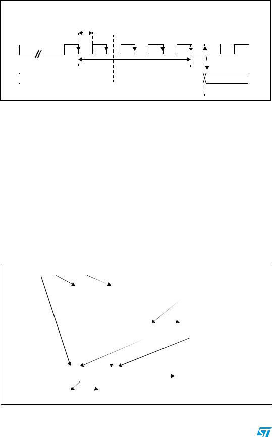
Figure 135. LIN synch field measurement
TMASTER = Master clock period |
|
|
|
|
|
|
|
|
|
|
||
TBR = Baud Rate period |
TBR = UARTDIV.TMASTER |
|
|
|
|
|
|
|||||
SM = Synch Measurement Register (19 bits) |
|
|
|
|
|
|
|
|
||||
|
TBR |
|
|
|
|
|
|
|
|
|
|
|
LIN Break |
|
|
|
LIN Synch Field |
|
|
|
|
Next |
|||
Start |
|
|
|
|
|
|
|
|
|
|||
Break |
Bit0 |
Bit1 |
Bit2 |
Bit3 |
Bit4 |
Bit5 |
Bit6 |
Bit7 |
Stop |
Start |
||
delim. |
Bit |
Bit |
Bit |
|||||||||
|
|
|
|
|
|
|
|
|||||
|
|
|
Measurement = 8.TBR = SM.TMASTER |
|
|
|
||||||
UARTDIV(n) |
|
|
|
|
|
|
|
|
UARTDIV(n+1) |
|||
|
UARTDIV = TBR / (TMASTER) = Rounding (SM / 128) |
|
|
|
||||||||
UARTDIV is an unsigned integer, coded in the BRR1 and BRR2 registers as shown in
Figure 119.
If LASE bit = 1 then UARTDIV is automatically updated at the end of each LIN Synch Field.
Three registers are used internally to manage the auto-update of the LIN divider (UARTDIV):
●UARTDIV_NOM (nominal value written by software at UART_BRR1 and UART_BRR2 addresses)
●UARTDIV_MEAS (results of the Field Synch measurement)
●UARTDIV (used to generate the local baud rate)
The control and interactions of these registers are explained in Figure 136 and Figure 137. They depend on the LDUM bit setting (LIN Divider Update Method)
As explained in Figure 136 and Figure 137, UARTDIV can be updated by two concurrent actions: a transfer from UARTDIV_MEAS at the end of the LIN Sync Field and a transfer from UARTDIV_NOM due to a software write to BRR1. If both operations occur at the same time, the transfer from UARTDIV_NOM has priority.
Figure 136. UARTDIV read / write operations when LDUM = 0
Write UART2_BRR1 |
Write UART2_BRR2 |
|
|
|
|||||
|
|
|
|
|
|
|
LIN Sync Field |
|
|
|
UARTDIV[11:4] |
UARTDIV[15:2] |
|
|
|||||
|
UARTDIV_NOM Measurement |
|
|||||||
|
|
|
UARTDIV[3:0] |
|
|
|
|
||
|
|
|
Write |
|
|
|
|
|
|
|
UART2_BRR1 |
|
UARTDIV[11:4] |
UARTDIV[15:12] |
|
UARTDIV_MEAS |
|||
|
|
|
|
|
|
|
UARTDIV[3:0] |
|
|
|
|
|
|
|
|
|
|
|
|
|
UARTDIV[7:0] |
UARTDIV[15:12] |
UARTDIV |
Baud Rate |
|
|
UARTDIV[3:0] |
|
|
||
|
|
||||
|
|
|
|
|
Generation |
Read UART2_BRR1 |
Read UART2_BRR2 |
|
|||
342/454 |
Doc ID 14587 Rev 9 |

RM0016 |
|
|
Universal asynchronous receiver transmitter (UART) |
|||||||||||||
|
|
|
|
|
|
|
|
|
|
|
|
|
|
|
|
|
Figure 137. UARTDIV read / write operations when LDUM = 1 |
|
|||||||||||||||
|
|
|
|
|
|
|
|
|
||||||||
|
Write UART2_BRR1 |
|
|
Write UART2_BRR2 |
|
|
|
|
||||||||
|
|
|
|
|
|
|
|
|
|
|
|
|
|
LIN Sync Field |
||
|
|
|
|
|
|
|
UARTDIV[15:12] |
|
|
|
||||||
|
|
|
UARTDIV[11:4] |
UARTDIV_NOM Measurement |
||||||||||||
|
|
|
|
|
|
|
UARTDIV[3:0] |
|
|
|
|
|
||||
|
|
|
|
|
|
RXNE=1 |
|
|
|
|
|
|
|
|
|
|
|
|
|
|
|
|
|
|
|
|
|
|
|
|
|||
|
|
|
|
|
|
|
|
|
UARTDIV[11:4] |
UARTDIV[15:12] |
|
UARTDIV_MEAS |
||||
|
|
|
|
|
|
|
|
|
|
|
|
|
|
UARTDIV[3:0] |
|
|
|
|
|
|
|
|
|
|
|
|
|
|
|
|
LDUM is reset |
|
|
|
|
|
|
|
|
|
|
|
|
|
|
|
|
|
||
|
|
|
|
|
|
|
|
|
|
|||||||
|
|
UARTDIV[11:4] |
UARTDIV[15:12] |
UARTDIV |
|
Baud Rate |
|
|||||||||
|
|
|
UARTDIV[3:0] |
|
|
|
Generation |
|
||||||||
|
Read UART2_BRR1 |
|
Read UART2_BRR2 |
|
|
|
|
|||||||||
|
|
|
|
|
|
|
|
|
|
|
|
|
|
|
|
|
Deviation error on the synch field
The deviation error is checked by comparing the current baud rate (relative to the slave oscillator) with the received LIN Synch Field (relative to the master oscillator). Two checks are performed in parallel.
The first check is based on a measurement between the first falling edge and the last falling edge of the Synch Field.
●If D1 > 14.84% LHE is set
●If D1< 14.06% LHE is not set
●If 14.06% < D1 < 14.84% LHE can be either set or reset depending on the dephasing between the signal on UART_RX pin and the fMASTER clock
The second check is based on a measurement of time between each falling edge of the Synch Field
●If D2 > 18.75% LHE is set
●If D2 < 15.62% LHE is not set
●If 15.62% < D2 < 18.75% LHE can be either set or reset depending on dephasing between the signal on UART_RX pin and the fMASTER clock
Note that the UART does not need to check if the next edge occurs slower than expected. This is covered by the check for deviation error on the full synch byte.
Doc ID 14587 Rev 9 |
343/454 |

Universal asynchronous receiver transmitter (UART) |
RM0016 |
|
|
|
|
Note: |
Deviation checking is based on the current baudrate and not on the nominal one. Therefore, |
|
|
in order to guarantee correct deviation checking, the baudrate generator must reload the |
|
|
nominal value before each new Break reception. This nominal value is programmed by the |
|
|
application during initialization. To do this software must set the LDUM bit before checksum |
|
|
reception. |
|
If LDUM bit is set, the next character reception will automatically reload the baudrate generator with nominal value.
You can also reload the nominal value by writing to BRR2 and BRR1. This second method is typically used when an error occurs during response transmission or reception.
If for any reason, the LDUM bit is set when UART is receiving a new Break and a Synch Field, this bit will be ignored and cleared. UART will adjust the baudrate generator with a value calculated from the synch field.
LIN header error detection
LHE is set if one of the following conditions occurs:
●Break Delimiter is too short
●Deviation error on the Synch Field is outside the LIN specification which allows up to +/ -14% of period deviation between the slave and master oscillators.
●Framing error in Synch Field or Identifier Field
●A LIN header reception time-out
●An overflow during the Synch Field Measurement, which leads to an overflow of the divider registers
LIN header time-out error
The description in the section LIN header time-out error on page 340 applies also when automatic resynchronization is enabled.
UART clock tolerance when synchronized
When synchronization has been performed, following reception of a LIN Break, the UART has the same clock deviation tolerance as in UART mode, which is explained below:
During reception, each bit is oversampled 16 times. The mean of the 8th, 9th and 10th samples is considered as the bit value.
Consequently, the clock frequency should not vary more than 6/16 (37.5%) within one bit.
The sampling clock is resynchronized at each start bit, so that when receiving 10 bits (one start bit, 1 data byte, 1 stop bit), the clock deviation should not exceed 3.75%.
344/454 |
Doc ID 14587 Rev 9 |

RM0016 |
Universal asynchronous receiver transmitter (UART) |
|
|
UART clock tolerance when unsynchronized
When LIN slaves are unsynchronized (meaning no characters have been transmitted for a relatively long time), the maximum tolerated deviation of the UART clock is +/-14%.
If the deviation is within this range then the LIN Break is detected properly when a new reception occurs.
This is made possible by the fact that masters send 13 low bits for the LIN Break, which can be interpreted as 11 low bits (13 bits -14% = 11.18) by a "fast" slave and then considered as a LIN Break. According to the LIN specification, a LIN Break is valid when its duration is greater than tSBRKTS = 10. This means that the LIN Break must last at least 11 low bits.
If the period desynchronization of the slave is +14% (slave too slow), the character "00h" which represents a sequence of 9 low bits must not be interpreted as a break character (9 bits + 14% = 10.26). Consequently, a valid LIN break must last at least 11 low bits.
Clock deviation causes
The causes which contribute to the total deviation are:
●DTRA: Deviation due to transmitter error. Note: the transmitter can be either a master or a slave (in case of a slave listening to the response of another slave).
●DMEAS: Error due to the LIN Synch measurement performed by the receiver.
●DQUANT: Error due to the baud rate quantization of the receiver.
●DREC: Deviation of the local oscillator of the receiver: This deviation can occur during the reception of one complete LIN message assuming that the deviation has been compensated at the beginning of the message.
●DTCL: Deviation due to the transmission line (generally due to the transceivers)
●All the deviations of the system should be added and compared to the UART clock tolerance:
– DTRA + DMEAS+ DQUANT + DREC + DTCL < 3.75%
Error due to LIN synch measurement
The LIN Synch Field is measured over eight bit times.
This measurement is performed using a counter clocked by the CPU clock. The edge detections are performed using the CPU clock cycle.
This leads to a precision of 2 CPU clock cycles for the measurement which lasts 8*UARTDIV clock cycles.
Consequently, this error (DMEAS) is equal to:
2 / (8*UARTDIVMIN)
UARTDIVMIN corresponds to the minimum LIN prescaler content, leading to the maximum baud rate, taking into account the maximum deviation of +/-14%.
Error due to baud rate quantization
The baud rate can be adjusted in steps of 1 / (UARTDIV). The worst case occurs when the "real" baud rate is in the middle of the step.
This leads to a quantization error (DQUANT) equal to 1 / (2*UARTDIVMIN).
Doc ID 14587 Rev 9 |
345/454 |