
- •ADSP-2192M DUAL CORE DSP FEATURES
- •FUNCTIONAL BLOCK DIAGRAM
- •DSP CORE FEATURES
- •TABLE OF CONTENTS
- •GENERAL DESCRIPTION
- •Figure 1. ADSP-219x DSP Core
- •DSP Core Architecture
- •DSP Peripherals
- •Memory Architecture
- •Figure 2. ADSP-2192M Internal/External Memory, Boot Memory, and I/O Memory Maps
- •Interrupts
- •DMA Controller
- •External Interfaces
- •PCI 2.2 Host Interface
- •USB 1.1 Host Interface
- •Sub-ISA Interface
- •CardBus Interface
- •AC’97 2.1 External Codec Interface
- •Serial EEPROM Interface
- •Internal Interfaces
- •Register Interface
- •Register Spaces
- •PCI Configuration Space
- •DSP Core Register Space
- •Peripheral Device Control Register Space
- •USB Register Space
- •CardBus Interface
- •Using the PCI Interface
- •Target/Slave Interface
- •Bus Master Interface
- •PCI Interrupts
- •PCI Control Register.
- •PCI Configuration Space
- •Similarities Between the Three PCI Functions
- •Interactions Between the Three PCI Configurations
- •PCI Memory Map
- •Figure 3. PCI Addressing for 24-Bit and 16-Bit Memory Blocks in 24-Bit Access (BAR2) Mode
- •Figure 4. PCI Addressing for 24-Bit and 16-Bit Memory Blocks in 16-Bit Access (BAR3) Mode
- •24-Bit PCI DSP Memory Map (BAR2)
- •16-Bit PCI DSP Memory Map (BAR3)
- •16-Bit PCI DSP I/O Memory Map (BAR4)
- •Using the USB Interface
- •USB DSP Register Definitions
- •USB DSP Memory Buffer Base Addr Register
- •USB DSP Memory Buffer Size Register
- •USB DSP Memory Buffer RD Pointer Offset Register
- •USB DSP Memory Buffer WR Pointer Offset Register
- •USB Descriptor Vendor ID
- •USB Descriptor Product ID
- •USB Descriptor Release Number
- •USB Descriptor Device Attributes
- •USB DSP MCU Register Definitions
- •USB Endpoint Description Register
- •USB Endpoint NAK Counter Register
- •USB Endpoint Stall Policy Register
- •USB Endpoint 1 Code Download Base Address Register
- •USB Endpoint 2 Code Download Base Address Register
- •USB Endpoint 3 Code Download Base Address Register
- •USB Endpoint 1 Code Current Write Pointer Offset Register
- •USB Endpoint 2 Code Current Write Pointer Offset Register
- •USB Endpoint 3 Code Current Write Pointer Offset Register
- •USB SETUP Token Command Register
- •USB SETUP Token Data Register
- •USB SETUP Counter Register
- •USB Register I/O Address Register
- •USB Register I/O Data Register
- •USB Control Register
- •USB Address/Endpoint Register
- •USB Frame Number Register
- •General USB Device Definitions
- •Configuration 0, 1, and 2 Device Definition
- •Endpoint 0 Definition
- •USB MCU Code Download
- •USB REGIO (Write)
- •USB REGIO (Read)
- •DSP Code Download
- •Example Initialization Process
- •USB Data Pipe Operations
- •OUT Transactions (Host to Device)
- •IN Transactions (Device to Host)
- •Sub-ISA Interface
- •PCI Interface to DSP Memory
- •USB Interface to DSP Memory
- •AC’97 Codec Interface to DSP Memory
- •Data FIFO Architecture
- •FIFO Control Registers
- •System Reset Description
- •Power-On Reset
- •DSP Software Reset
- •Booting Modes
- •Figure 5. Boot Process Flow
- •Power Management Description
- •Power Regulators
- •Low Power Operation
- •Clock Signals
- •Figure 7. External Crystal Connections
- •Figure 8. Clock Domains
- •Instruction Set Description
- •Development Tools
- •Designing an Emulator-Compatible DSP Board (Target)
- •Target Board Header
- •Figure 9. JTAG Target Board Connector for JTAG Equipped Analog Devices DSP (Jumpers in Place)
- •Figure 10. JTAG Target Board Connector with No Local Boundary Scan
- •JTAG Emulator Pod Connector
- •Figure 11. JTAG Pod Connector Dimensions
- •Figure 12. JTAG Pod Connector Keep-Out Area
- •Design-for-Emulation Circuit Information
- •Additional Information
- •PIN DESCRIPTIONS
- •SPECIFICATIONS
- •ABSOLUTE MAXIMUM RATINGS
- •ESD SENSITIVITY
- •TIMING SPECIFICATIONS
- •Programmable Flags Cycle Timing
- •Figure 13. Programmable Flags Cycle Timing
- •Sub-ISA Interface Read/Write Cycle Timing
- •Figure 14. Sub-ISA Interface Read Cycle Timing
- •Figure 15. Sub-ISA Interface Write Cycle Timing
- •Output Drive Currents
- •Figure 16. Typical Drive Currents
- •Power Dissipation
- •Test Conditions
- •Output Disable Time
- •Figure 17. Output Enable/Disable
- •Figure 18. Equivalent Device Loading for AC Measurements (Includes All Fixtures)
- •Figure 19. Voltage Reference Levels for AC Measurements (Except Output Enable/Disable)
- •Output Enable Time
- •Example System Hold Time Calculation
- •Capacitive Loading
- •Environmental Conditions
- •144-Lead LQFP Pinout
- •OUTLINE DIMENSIONS
- •ORDERING GUIDE

ADSP-2192M
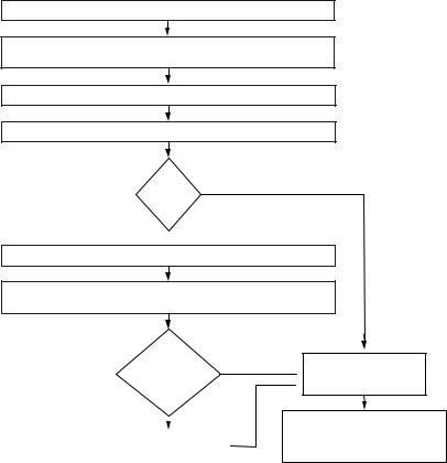
Optionally, extra boot information can come from an SPI or Microwire serial EPROM during PCI or USB booting. The boot process flow appears in Figure 5.
DSP EMERGES FROM RESET AND PROGRAM FLOW JUMPS TO BOOT ROM
LOADER KERNEL READS CRST PINS AND DETERMINES MODE OF BOOTING.
ALSO PERFORMS HOUSEKEEPING OPERATIONS, SETTING UP INTERRUPTS, ETC.
CALL SUBROUTINE TO AUTO-DETECT SERIAL EEPROM
LOADER KERNEL READS BUS MODE PINS TO SET UP BUS CONFIGURATION
SERIAL NO
EEPROM
EXISTS?
YES
DETERMINE 8- OR 16-BIT SPI OR MICROWIRE
LOAD SERIAL EEPROM CONFIGURATION AND DATA PACKETS.
LOAD PCI/USB CONFIGURATION REGISTERS ACCORDINGLY
DOES ANY SERIAL |
NO |
|
|
||
EEPROM NEED TO |
|
|
BE EXECUTED? |
|
|
|
YES |
|
|
|
|
|
|
|
EXECUTE PACKETS |
|
|
|
|
|
Figure 5. Boot Process Flow
TRANSFER CONTROL TO PCI OR USB, TO FACILITATE
REST OF BOOT
AFTER BOOTING IS COMPLETE, USER HAS OPTION TO RETURN TO SERIAL EEPROM OR JUMP TO USER CODE AND BEGIN EXECUTION
FINISH
Power Management Description
The ADSP-2192M supports several states with distinct power management and functionality capabilities. These states encompass both hardware and software states.
The driver and DSP code take responsibility for detailed power management of the modem, so minimum power levels are achieved regardless of OS or BIOS. In response to events, the driver and DSPs manage power by changing platform states as necessary.
Power Regulators
The ADSP-2192M is intended to operate in a variety of different systems. These include PCI, CardBus, USB, and embedded (Sub-ISA) applications. The PCI and USB specifications define power consumption limits that constrain the design of the DSP.
2.5 V Regulator Options
In 5 V and 3.3 V PCI applications the ADSP-2192M 2.5 V IVDD supply will be generated by an on-chip regulator. The internal 2.5 V supply (IVDD) can be generated by the on-chip regulator combined with an external power transistor as shown in Figure 6. To support the PCI specification’s power-down modes, the two transistors control the primary and auxiliary supply. If the reference voltage on RVDD (typically the same as PCIVDD) drops out, the VCTRLAUX will switch on the device connected to PCIVAUX and VCTRLVDD will switch off the primary supply. USB applications may require an external high efficiency switching regulator to generate the 2.5 V supply for the ADSP-2192M.
–24– |
REV. 0 |