

ADSP-TS101S
The ADSP-TS101S core always exits from reset in the idle state and waits for an interrupt. Some of the interrupts in the interrupt vector table are initialized and enabled after reset.
Low Power Operation
The ADSP-TS101S can enter a low power sleep mode in which its core does not execute instructions, reducing power consump-
tion to a minimum. The ADSP-TS101S exits sleep mode when it senses a falling edge on any of its IRQ3–0 interrupt inputs. The
interrupt, if enabled, causes the ADSP-TS101S to execute the corresponding interrupt service routine. This feature is useful for systems that require a low power standby mode.
Clock Domains
The ADSP-TS101S has two clock inputs that drive its two major clock domains:
•SCLK (system clock). Provides clock input for the external bus interface and defines the ac specification
reference for the external bus signals. The external bus interface runs at 1× the SCLK frequency. A DLL locks internal SCLK to SCLK input. The maximum SCLK frequency is the minimum of either 100 MHz or CCLK/2, where CCLK is the internal DSP clock frequency. SCLK must be connected to the same clock source as LCLK.
•LCLK (local clock). Provides clock input to the internal clock driver, CCLK, which is the internal clock for the core, internal buses, memory, and link ports. The instruction execution rate is equal to CCLK. A PLL from LCLK generates CCLK which is phase-locked. The LCLKRAT pins define the clock multiplication of LCLK to CCLK (see Table 4 on Page 12). The link port clock is generated from CCLK via a software programmable divisor.
RESET must be asserted until LCLK is stable and within specification for at least 2 ms. This applies to power-up as well as any dynamic modification of LCLK after power-
up. Dynamic modification may include LCLK going out of specification as long as RESET is asserted.
Connecting SCLK and LCLK to the same clock source is a requirement for the device. Using an integer clock multiplication value provides predictable cycle-by-cycle operation, a requirement of fault-tolerant systems and some multiprocessing systems.
Power Supplies
The ADSP-TS101S has separate power supply connections for internal logic (VDD), analog circuits (VDD_A), and I/O buffer (VDD_IO) power supply. The internal (VDD) and analog (VDD_A) supplies must meet the 1.2 V requirement. The I/O buffer (VDD_IO) supply must meet the 3.3 V requirement.
The analog supply (VDD_A) powers the clock generator PLLs. To produce a stable clock, systems must provide a clean power supply to power input VDD_A. Designs must pay critical attention to bypassing the VDD_A supply.
CROSSCORE is a trademark of Analog Devices, Inc.
VisualDSP++ is a trademark of Analog Devices, Inc.
The ideal power-on sequence for the DSP is to provide powerup of all supplies simultaneously. If there is going to be some delay between power-up of the supplies, provide VDD (and VDD_A) first, then VDD_IO.
Filtering Reference Voltage and Clocks
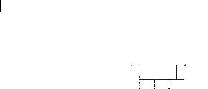
Figure 5 shows a possible circuit for filtering VREF, SCLK_N, and LCLK_N. This circuit provides the reference voltage for the switching voltage, system clock, and local clock references.
VDD_IO |
VREF |

 SCLK_N
R1
 LCLK_N
R2 |
C1 |
C2 |
VSS
R1: 2k SERIES RESISTOR
R2: 1.67k SERIES RESISTOR
C1: 1 F CAPACITOR (SMD)
C2: 1nF CAPACITOR (HF SMD) PLACED CLOSE TO DSP’S PINS
Figure 5. VREF, SCLK_N, and LCLK_N Filter
Development Tools
The ADSP-TS101S is supported with a complete set of CROSSCORE™ software and hardware development tools, including Analog Devices emulators and VisualDSP++™ development environment. The same emulator hardware that supports other TigerSHARC DSPs also fully emulates the ADSP-TS101S.
The VisualDSP++ project management environment lets programmers develop and debug an application. This environment includes an easy to use assembler (which is based on an algebraic syntax), an archiver (librarian/library builder), a linker, a loader, a cycle-accurate instruction-level simulator, a C/C++ compiler, and a C/C++ runtime library that includes DSP and mathematical functions. A key point for these tools is C/C++ code efficiency. The compiler has been developed for efficient translation of C/C++ code to DSP assembly. The DSP has architectural features that improve the efficiency of compiled C/C++ code.
The VisualDSP++ debugger has a number of important features. Data visualization is enhanced by a plotting package that offers a significant level of flexibility. This graphical representation of user data enables the programmer to quickly determine the performance of an algorithm. As algorithms grow in complexity, this capability can have increasing significance on the designer’s development schedule, increasing productivity. Statistical profiling enables the programmer to nonintrusively poll the processor as it is running the program. This feature, unique to VisualDSP++, enables the software developer to passively gather important code execution metrics without interrupting the realtime characteristics of the program. Essentially, the developer can identify bottlenecks in software quickly and efficiently. By using the profiler, the programmer can focus on those areas in the program that impact performance and take corrective action.
REV. 0 |
–9– |