

ADSP-TS201S
ADSP-TS201S—SPECIFICATIONS
Note that component specifications are subject to change without notice. For information on Link port electrical characteristics, see Link Port Low-Voltage, Differential-Signal (LVDS) Electrical Characteristics and Timing on Page 30.
RECOMMENDED OPERATING CONDITIONS
Parameter |
Test Conditions |
Grade1 |
Min |
Typ |
Max |
Unit |
|
|
|
|
|
|
|
|
|
VDD |
Internal Supply Voltage |
@ CCLK = 600 MHz |
060 |
1.14 |
1.20 |
1.26 |
V |
|
|
|
|
|
|
|
|
|
|
@ CCLK = 500 MHz |
050 |
1.00 |
1.05 |
1.10 |
V |
VDD_A |
Analog Supply Voltage |
@ CCLK = 600 MHz |
060 |
1.14 |
1.20 |
1.26 |
V |
|
|
|
|
|
|
|
|
|
|
@ CCLK = 500 MHz |
050 |
1.00 |
1.05 |
1.10 |
V |
VDD_IO |
I/O Supply Voltage |
|
(all) |
2.38 |
2.50 |
2.63 |
V |
|
Internal DRAM Supply Voltage |
@ CCLK = 600 MHz |
060 |
1.52 |
1.60 |
1.68 |
V |
VDD_DRAM |
|
@ CCLK = 500 MHz |
050 |
1.425 |
1.500 |
1.575 |
V |
TCASE |
Case Operating Temperature |
|
A |
–40 |
|
+85 |
°C |
TCASE |
Case Operating Temperature |
|
W |
–40 |
|
+105 |
°C |
VIH1 |
High Level Input Voltage2 |
@ VDD, VDD_IO = max |
(all) |
1.7 |
|
|
V |
VIH2 |
High Level Input Voltage3 |
@ VDD, VDD_IO = max |
(all) |
1.9 |
|
|
V |
VIL |
Low Level Input Voltage4 |
@ VDD, VDD_IO = min |
(all) |
|
|
0.8 |
V |
IDD |
VDD Supply Current, Typical Activity5 |
@ CCLK = 600 MHz, VDD = 1.20 V, TCASE = 25ºC |
060 |
|
2.61 |
|
A |
|
|
@ CCLK = 500 MHz, VDD = 1.05 V, TCASE = 25ºC |
050 |
|
2.06 |
|
A |
IDD_A |
VDD_A Supply Current, Typical Activity |
@ CCLK = 600 MHz, VDD = 1.20 V, TCASE = 25ºC |
060 |
|
25 |
55 |
mA |
|
|
|
|
|
|
||
|
|
@ CCLK = 500 MHz, VDD = 1.05 V, TCASE = 25ºC |
050 |
|
20 |
50 |
mA |
IDD_IO |
VDD_IO Supply Current, Typical Activity 5 |
@ SCLK = 62.5 MHz, VDD_IO = 2.5 V, TCASE = 25ºC |
(all) |
|
0.15 |
|
A |
IDD_DRAM |
VDD_DRAM Supply Current, Typical Activity5 |
@ CCLK = 600 MHz, VDD_DRAM = 1.6 V, TCASE = 25ºC |
060 |
|
0.28 |
0.43 |
A |
|
|
@ CCLK = 500 MHz, VDD_DRAM = 1.5 V, TCASE = 25ºC |
050 |
|
0.25 |
0.40 |
A |
VREF |
Voltage Reference |
|
(all) |
(VDD_IO ×0.59)±5% |
V |
||
SCLK_VREF |
Voltage Reference |
|
(all) |
(VCLOCK_DRIVE ×0.59)±5% |
V |
||
|
|
|
|
|
|
|
|
1 Specifications vary for different grades (for example, SABP-060, SABP-050, SWBP-050). For more information on part grades, see Ordering Guide on Page 44.
2VIH1 specification applies to input and bidirectional pins: SCLKRAT2–0, SCLK, ADDR31–0, DATA63–0, RD, WRL, WRH, ACK, BRST, BR7–0, BOFF, HBR, HBG, MSSD3–0, RAS, CAS, SDCKE, SDWE, TCK, FLAG3–0, DS2–0, ENEDREG.
3 VIH2 specification applies to input and bidirectional pins: TDI, TMS, TRST, CIMP1–0, ID2–0, LxBCMPI, LxACKI, POR_IN, RST_IN, IRQ3–0, CPA, DPA, DMAR3–0. 4 Applies to input and bidirectional pins.
5For details on internal and external power calculation issues, including other operating conditions, see the EE-170, Estimating Power for the ADSP-TS201S on the Analog Devices website.
Rev. 0 | Page 21 of 44 | November 2004
ADSP-TS201S
ELECTRICAL CHARACTERISTICS
Parameter |
|
Test Conditions |
Min |
Max |
Unit |
|
|
|
|
|
|
VOH |
High Level Output Voltage1 |
@VDD_IO = min, IOH = –2 mA |
2.18 |
|
V |
VOL |
Low Level Output Voltage1 |
@VDD_IO = min, IOL = 4 mA |
|
0.4 |
V |
IIH |
High Level Input Current |
@VDD_IO = max, VIN = VIH max |
|
20 |
µA |
IIH_PU |
High Level Input Current |
@VDD_IO = max, VIN = VIH max |
|
50 |
µA |
IIH_PD |
High Level Input Current |
@VDD_IO = max, VIN = VDD_IO max |
0.3 |
0.76 |
mA |
IIH_PD_I |
High Level Input Current |
@VDD_IO = max, VIN = VIH max |
30 |
76 |
µA |
IIL |
Low Level Input Current |
@VDD_IO = max, VIN = 0 V |
|
20 |
µA |
IIL_PU |
Low Level Input Current |
@VDD_IO = max, VIN = 0 V |
0.3 |
0.76 |
mA |
IIL_PU_AD |
Low Level Input Current |
@VDD_IO = max, VIN = 0 V |
30 |
100 |
µA |
IOZH |
Three-State Leakage Current High |
@VDD_IO = max, VIN = VIH max |
|
20 |
µA |
IOZH_PD |
Three-State Leakage Current High |
@VDD_IO = max, VIN = VDD_IO max |
0.3 |
0.76 |
mA |
IOZL |
Three-State Leakage Current Low |
@VDD_IO = max, VIN = 0 V |
|
20 |
µA |
IOZL_PU |
Three-State Leakage Current Low |
@VDD_IO = max, VIN = 0 V |
0.3 |
0.76 |
mA |
IOZL_PU_AD |
Three-State Leakage Current Low |
@VDD_IO = max, VIN = 0 V |
30 |
100 |
µA |
IOZL_OD |
Three-State Leakage Current Low |
@VDD_IO = max, VIN = 0 V |
4 |
7.6 |
mA |
CIN |
Input Capacitance2, 3 |
@fIN = 1 MHz, TCASE = 25ºC, VIN = 2.5 V |
|
3 |
pF |
Parameter name suffix conventions: no suffix = applies to pins without pull-up or pull-down resistors, _PD = applies to pin types (pd) or (pd_0), _PU = applies to pin types (pu) or (pu_0), _PU_AD = applies to pin types (pu_ad), _OD = applies to pin types OD
1 Applies to output and bidirectional pins.
2 Applies to all signals.
3 Guaranteed but not tested.
Rev. 0 | Page 22 of 44 | November 2004
ADSP-TS201S
ABSOLUTE MAXIMUM RATINGS
Internal (Core) Supply Voltage (VDD)1 |
–0.3 V to +1.40 V |
Analog (PLL) Supply Voltage (VDD_A)1 |
–0.3 V to +1.40 V |
External (I/O) Supply Voltage (VDD_IO)1 |
–0.3 V to +3.5 V |
External (DRAM) Supply Voltage (VDD_DRAM)1 |
–0.3 V to +2.1 V |
Input Voltage1 |
–0.5 V to +3.63 V |
Output Voltage Swing1 |
–0.5 V to VDD_IO +0.5 V |
Storage Temperature Range1 |
–65ºC to +150ºC |
1Stresses greater than those listed above may cause permanent damage to the device. These are stress ratings only. Functional operation of the device at these or any other conditions greater than those indicated in the operational sections of this specification is not implied.
Exposure to absolute maximum rating conditions for extended periods may affect device reliability.
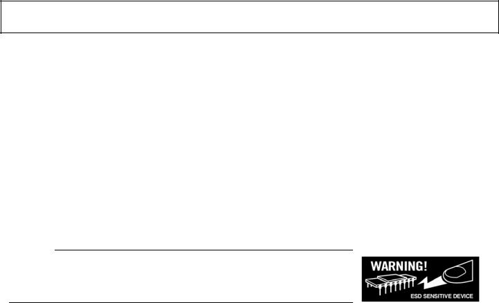
ESD SENSITIVITY
CAUTION
ESD (electrostatic discharge) sensitive device. Electrostatic charges as high as 4000 V readily accumulate on the human body and test equipment and can discharge without detection. Although the ADSP-TS201S features proprietary ESD protection circuitry, permanent damage may occur on devices subjected to high-energy electrostatic discharges. Therefore, proper ESD precautions are recommended to avoid performance degradation or loss of functionality.
Rev. 0 | Page 23 of 44 | November 2004