


Verilog
6. Finite State Machine Synthesis
6.1. Verilog template
A finite state machine can be “hidden” in a Verilog description. Such a finite state machine description contains at least one sequential always block declaration or at most two always blocks: a sequential one and a combinational one. The sensitivity list of the sequential always block must contain at least one signal which is the clock signal and at most two signals which are the clock and the reset signals. For the clock a rising or a falling edge can be declared. The reset is not mandatory. If it is declared, it has to be an asynchronous signal. In the sequential always block, an “if” statement specifies an asynchronous reset if it exists and a synchronous part assigning the state variable.
6.1.1. State register and next state equations
•The state variables have to be assigned within the sequential always block.
•The type of the state register can be integer or bit_vector.
•The next state equations must be described in the sequential always block using a "case" statement or outside the always block like the non latched outputs.
6.1.2. Latched and non latched outputs
•The non latched outputs must be described in a combinational always block or using data flow conditional statements ("assign <output> = <condition> ? <value>:
...").
•The latched outputs must be assigned within the sequential always block like the state register.
•Note that presently the vectored outputs are not recognized as outputs of the FSM.
6.1.3. Latched inputs
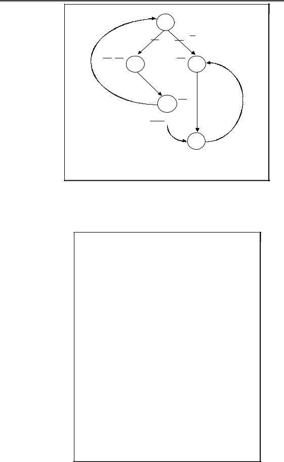
• The latched inputs must be described using internal signals representing the output of the flip-flops. These internal signals have then to be assigned in a sequential always block with the latched inputs. This sequential always block must be the one where the state register is assigned as showed in figure 58. Figure 58 gives the Verilog description of the FSM described in figure 56 where the two inputs A and B are latched.
The figure 56 represents a Moore FSM. This FSM has two outputs: Z0 which is a latched output and Z1 which is a non latched output. This machine will be described twice. The first description uses a simple sequential always block (cf. figure 57). The second description uses both a sequential always block and a combinational one (cf. figure 58).
Verilog - 31
Verilog
|
|
|
1 |
Z0 Z1 |
|
|
|
|
|
|
|
|
|
A |
|
|
A |
Z0 |
Z1 |
2 |
|
Z1 |
3 |
A+B |
4 Z1 |
A+B 
 Z1
Z1
5
Z0 is a latched output
Z1 is a non latched output
Figure 56: Graphical representation of a Moore FSM
The FSM represented in figure 56 is described in figure 57 using a sequential always block for the state register, the latched output Z0 and the next state logic, and a conditional assignment for the output Z1.
module FSM ( RESET, CLOCK, A, B, Z0, Z1); input RESET, CLOCK, A, B;
output Z0, Z1; reg Z0;
integer STATE;
always @(posedge CLOCK or posedge RESET) if (RESET == 1’b1)
STATE = 1;
else
case (STATE) 1: begin
Z0 = 1’b1; if (A)
STATE = 2;
else
STATE = 3;
end
2: begin
Z0 = 1’b0; STATE = 4;
end
3:STATE = 5;
4:if (A | B)
STATE = 1;
else
STATE = 5;
5:STATE = 3;
Verilog - 32
Verilog
default: STATE = 1;
endcase
assign Z1 = (STATE == 1); // Z1 is not latched endmodule
Figure 57: Verilog description of a Moore FSM
Note that in figure 57, the "case" statement describing the next state logic and the state register assignment in the sequential always block has a "default" branch. In this branch the state register must be assigned to the reset value and this value is used for simplification.
The FSM represented in figure 56 is described in figure 58 using a sequential always block for the state register and the latched output Z0, and a combinational always block for the output Z1 and the next state logic.
module FSM ( RESET, CLOCK, A, B, Z0, Z1); input RESET, CLOCK, A, B;
output Z0, Z1; reg Z0, Z1;
integer STATE, NEXTSTATE;
always @( posedge CLOCK or posedge RESET) if (RESET == 1’b1)
STATE = 1;
else
begin
STATE = NEXTSTATE; case (STATE)
1: Z0 = 1’b1; 2: Z0 = 1’b0;
endcase
end
always @( A or B or STATE) begin
Z1 = 1’b0; // default value case (STATE)
1: begin
Z1 = 1'b1; if (A)
NEXTSTATE = 2;
else
NEXTSTATE = 3;
end
2:NEXTSTATE = 4;
3:NEXTSTATE = 5;
4:if (A | B)
NEXTSTATE = 1;
else
NEXTSTATE = 5; 5: NEXTSTATE = 3; default: NEXTSTATE = 1;
endcase
end endmodule
Figure 58: Verilog description of a Moore FSM
Verilog - 33

Verilog
Figure 59 gives the Verilog description of the FSM described in figure 56. In this description, the inputs A and B are latched.
module FSM ( RESET, CLOCK, A, B, Z0, Z1); input RESET, CLOCK, A, B;
output Z0, Z1; reg Z0;
integer VALUE; reg A_FF, B_FF;
always @( posedge CLOCK or posedge RESET) begin
if (RESET == 1’b1) VALUE = 1;
else begin
case (VALUE) 1: begin
Z0 = 1’b1;
if (A_FF == 1’b1) VALUE = 2;
else
VALUE = 3;
end
2: begin
Z0 = 1’b0; VALUE = 4;
end
3:VALUE = 5;
4:if (A_FF | B_FF) VALUE = 1;
else
VALUE = 5; 5: VALUE = 3; default: VALUE = 1;
endcase |
|
A_FF = A; |
// A_FF is latched |
B_FF = B; |
// B_FF is latched |
end
end
assign Z1 = (VALUE == 1); // Z1 is not latched endmodule
Figure 59: Verilog description of a Moore FSM with latched inputs
Verilog - 34