


DMA Ports 11
11.3.4IDMA Timing
From the host system interface point of view, there are three IDMA port operations with critical timing parameters. These operations are:
•latching the IDMA internal memory address,
•reading from the IDMA port, and
•writing to the IDMA port.
The following sections cover the timing details of each of these operations.
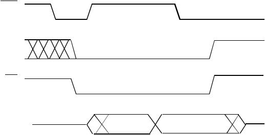
11.3.4.1 Address Latch Cycle
The host writes the DMA starting address and destination memory type (DM or PM) using the IDMA address latch cycle. The address latch cycle, shown in Figure 11.9, consists of the following steps:
1.Host ensures that IACKline is low.
2.Host asserts IAL and IS, directing the ADSP-2181 to latch the IDMA starting address from the IAD15-0 address/data bus into the IDMA Control Register.
3.Host drives the starting address (bits 0-13) and destination memory type (bit 14) onto the IAD15-0 bus. (Bit 15 must be a 0.)
Note that IRDand IWRremain high (inactive) throughout the latch operation.
IACK
IAL
IS
IAD15-0 |
ADDRESS |
Figure 11.9 IDMA Address Latch Cycle Timing
11 – 17

11 DMA Ports
Note: The IDMA starting address and destination memory type is available to the host and to the ADSP-2181 in the IDMA Control Register. For Data Memory accesses, the ADSP-2181 increments the address automatically after each IDMA read or write transfer (16-bit word). For Program Memory accesses, the ADSP-2181 increments the address automatically after each pair of IDMA read or write transfers (24-bit word).
Warning: Both the ADSP-2181 and the host can specify the starting address by writing to the IDMA Control Register. Do not let the ADSP-2181 access the IDMA Control Register while it is being written by the host; this operation will have an indeterminate result.
11.3.4.2 Long Read Cycle
The host reads the contents of an ADSP-2181 internal memory location using the IDMA port long read cycle. The read cycle, shown in Figure 11.10, consists of the following steps:
1.Host ensures that IACKline is low.
2.Host asserts IRDand IS(low), causing the ADSP-2181 to put the contents of the location pointed to by the IDMA address on the IAD15-0 address/data bus.
3.ADSP-2181 deasserts IACKline, indicating the requested data is being
fetched. When the ADSP-2181 asserts the IACKline, the requested data is driven on the IAD address/data bus.
4.Host detects the IACKline is now low and reads the data (READ DATA) from the IAD15-0 address/data bus. After reading the data, the host deasserts IRDand IS.
Note that IAL is low (inactive) and IWRis high (inactive) throughout the read operation.
IDMA memory accesses “steal” one processor cycle, but may only occur on instruction cycle boundaries. The best-case response for a 16-bit Data Memory read or the first 16 bits of a Program Memory read is 2.5 processor cycles; worst case is 3.5 cycles. One cycle is for synchronization, one is for reading the memory internally, and one-half cycle is for IACKsetup time. A second cycle of synchronization may be required. Thus the best-case and worst-case response times are determined as follows:
Best Case: 1 cycle (sync) + 1 cycle (internal memory read) + 0.5 cycle (IACK setup) = 2.5 cycles
Worst Case: 1 cycle (sync) + 1 cycle (sync) + 1 cycle (internal memory read) + 0.5 cycle ( IACKsetup) = 3.5 cycles
11 – 18
DMA Ports 11
IACK
IS
IRD
IAD15-0 |
PREVIOUS |
READ |
DATA |
DATA |
Figure 11.10 IDMA Long Read Cycle Timing
In the case of a Program Memory operation, the second IDMA port read cycle for a given internal 24-bit word does not require an internal memory access, does not wait for an instruction cycle boundary, and takes 1.5 or 2.5 cycles.
The bestand worst-case response times given above assume no system hold offs.
Hold offs for DMA transfers are defined in the section “DMA Cycle Stealing, DMA Hold Offs, and IACKAcknowledge” at the end of this chapter.
Warning: If an IDMA address latch cycle or an ADSP-2181 write to the IDMA Control Register occurs after a first Program Memory read cycle (16 bits), the IDMA port will lose the second half of the Program Memory word. The ADSP-2181 treats the next IDMA access as the first operation for the new IDMA address and destination.
11 – 19

11 DMA Ports
11.3.4.3 Short Read Cycle
The host reads the contents of a ADSP-2181 internal memory location using the IDMA short read cycle. The read cycle, shown in Figure 11.11, consists of the following steps:
1.Host ensures that IACKline is low.
2.Host asserts IRDand IS(low), directing the ADSP-2181 to put the contents of the location pointed to by the target IDMA address on the IAD15-0 address/data bus.
3.ADSP-2181 deasserts IACKline, indicating the requested data is being fetched.
4.Host detects the IACKline is now high and reads the data (PREVIOUS DATA) from the IAD15-0 address/data bus, before the requested data (READ DATA) is driven on the IAD address/data bus—not waiting for the ADSP-2181 to assert the IACKline. After reading the data, the host deasserts IRDand IS.
The host must do an initial “dummy” read, to make the ADSP-2181 put the first data word (PREVIOUS DATA) on the IAD15-0 bus.
Note that IAL is low (inactive) and IWRis high (inactive) throughout the read operation.
The IDMA Short Read and Long Read cycles provide different alternatives for implementing your DMA transfers. Short reads are useful for hosts that can handle the faster timing of these accesses, while long reads allow slower hosts more time.
The IDMA short read cycle also serves as a single-location data buffer. If you are using the ADSP-2181 in a multiprocessing environment, using this buffer is one way to avoid tying up the IAD bus (waiting for IACKsignal).
Warning: If an IDMA address latch cycle or a ADSP-2181 write to the IDMA Control register occurs after a first Program Memory read cycle, the IDMA port will lose the second half of the Program Memory word. The ADSP-2181 treats the next host data on the IAD address/data bus as the new contents of the IDMA Control Register.
11 – 20