- •10.1 OVERVIEW
- •10.2 PROGRAM MEMORY INTERFACE
- •10.2.1 External Program Memory Read / Write
- •10.2.2 Program Memory Maps
- •10.2.3 ROM Program Memory Maps
- •10.3 DATA MEMORY INTERFACE
- •10.3.1 External Data Memory Read/Write
- •10.3.2 Data Memory Maps
- •10.4 BOOT MEMORY INTERFACE
- •10.4.1 Boot Pages
- •10.4.2 Powerup Boot & Software Reboot
- •10.4.3 Boot Memory Access
- •10.4.4 Boot Loading Sequence
- •10.5 BUS REQUEST / GRANT
- •10.6.6 External Memory Read – Overlays & I/O Memory
- •10.6.7 External Memory Write – Overlays & I/O Memory
Memory Interface  10
10
10.1OVERVIEW
The ADSP-2100 family has a modified Harvard architecture in which data memory stores data and program memory stores both instructions and data. Each processor contains on-chip RAM and/or ROM, so that a portion of the program memory space and a portion of the data memory space reside on-chip. Each processor (except the ADSP-2181) also has a boot memory space in addition to the data and program spaces. The ADSP-2181 has a byte memory space instead of the boot memory space. The boot memory space and byte memory space can be used to load onchip program memory with code from an external EPROM at reset.
In each ADSP-2100 family device, memory is connected with the internal functional units by four on-chip buses: the data memory address bus (DMA), data memory data bus (DMD), program memory address bus (PMA), and program memory data bus (PMD). The internal PMA bus and DMA bus are multiplexed into a single address bus which is extended offchip. Likewise, the internal PMD bus and DMD bus are multiplexed into a single external data bus. The sixteen MSBs of the external data bus are used as the DMD bus: external bus lines D23-8 are used for DMD15-0.
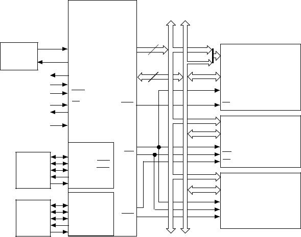
There are three separate memory spaces: data memory, program memory and boot (or byte) memory. The PMS, DMS, and BMSsignals indicate which memory space is being accessed. Because the program memory and data memory buses are multiplexed off-chip, if more than one external transfer must be made in the same instruction there will be an overhead cycle required. There is no overhead if just one off-chip access (with no wait states) occurs in any instruction. Figure 10.1 shows the external memory buses and control signals (for all ADSP-21xx processors except the ADSP-2181).
All external memories may have automatic wait state generation associated with them. The number of wait states—each equal to one instruction cycle—is programmable.
10 – 1

10 Memory Interface
This chapter includes example timing diagrams for the memory interfaces of the ADSP-21xx processors. For each bus transaction, only the sequence of events is described; you must consult the processor data sheets for actual timing parameters. All timing diagrams use CLKOUT as a reference, which indicates the instruction execution rate.
The memory interfaces of the ADSP-2181 are described separately in the second half this chapter.
|
ADSP-21xx |
|
|
|
|||
1x CLOCK |
|
|
|
14 |
A13-0 |
|
|
CLKIN |
|
|
ADDR13-0 |
|
ADDR |
BOOT |
|
or |
|
|
D23-22 |
||||
XTAL |
|
|
|
MEMORY |
|||
CRYSTAL |
|
|
|
|
|
||
|
|
|
|
D15-8 |
|
|
|
|
CLKOUT |
|
24 |
|
|
||
|
|
DATA23-0 |
|
DATA |
e.g. EPROM |
||
|
|
|
|
|
|||
|
RESET |
|
|
|
|
OE |
2764 |
|
IRQ2 |
|
|
|
|
27128 |
|
|
|
|
|
|
|
27256 |
|
|
BR |
|
|
|
|
|
|
|
|
|
BMS |
|
CS |
27512 |
|
|
BG |
|
|
|
A13-0 |
|
|
|
|
|
|
|
ADDR |
|
|
|
MMAP |
|
|
|
D23-0 |
PROGRAM |
|
|
|
|
|
|
|||
|
|
|
|
|
DATA |
||
|
|
|
|
|
|
MEMORY |
|
|
SPORT 1 |
RD |
|
OE |
(OPTIONAL) |
||
SERIAL |
SCLK1 |
|
|
WR |
|
WE |
|
|
|
|
|
CS |
|
||
DEVICE |
RFS1 or |
IRQ0 |
A13-0 |
|
|||
(OPTIONAL) |
TFS1 or |
IRQ1 |
|
|
|||
DT1 or |
FO |
|
|
ADDR |
DATA |
||
|
|
D23-8 |
|||||
|
DR1 or |
FI |
|
DATA |
MEMORY |
||
|
|
|
|
|
|
||
SERIAL |
SPORT 0 |
|
|
OE |
& |
||
SCLK0 |
|
|
PMS |
|
PERIPHERALS |
||
|
|
|
WE |
||||
DEVICE |
RFS0 |
|
|
DMS |
|
|
|
(OPTIONAL) |
TFS0 |
|
|
|
CS |
(OPTIONAL) |
|
DT0 |
|
|
|
|
|
|
|
|
|
|
|
|
|
|
|
|
DR0 |
|
|
|
|
|
|
NOTES
1.Applies to all ADSP-21xx processors except ADSP-2181.
2.ADSP-2171 and ADSP-21msp58/59 use a 1/2x CLKIN signal.
3.Unused data bus lines may be left floating.
4.The two MSBs of the data bus (D23-22) are used to supply the two MSBs of the boot memory EPROM address. This is only required for the 27256 and 27512.
Figure 10.1 ADSP-21xx System With External Memory
10 – 2
