

13 Hardware Examples
13.5SERIAL PORT TO ADC INTERFACE
An ADC (analog-to-digital converter) converts an analog signal to digital samples that a DSP processor can operate on. The ADSP-21xx processors can receive data from an ADC directly through a serial port.
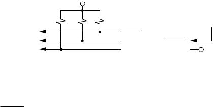
Analog Devices’ AD7872 is an ADC that requires no extra logic to interface to the SPORT. The AD7872 converts an analog signal to 14-bit samples. Each sample is padded with two zero MSBs to yield 16-bit samples. The AD7872 outputs each sample serially, MSB first. Its digital interface consists of three pins: SDATA, the serial data output; SCLK, for clocking data out; and SSTRB, (serial strobe), which frames each serial word.
The serial port connection to the AD7872 is shown in Figure 13.6. The timer regulates sampling via the CONVSTinput at a constant frequency. Instead of the timer, an unused serial clock or flag output from the ADSP21xx processor can be programmed to generate the CONVSTsignal. The AD7872 generates SCLK internally and provides it to the processor. With the CONTROL input held at –5 V, the SCLK signal is continuous, running even when no data is being output.
|
|
+5 V |
|
|
|
|
|
|
|
4.7 kΩ 2 kΩ |
4.7 kΩ |
|
|
|
|
ADSP-21xx |
|
|
AD7872 |
|
TIMER |
||
|
|
|
|
|
|||
|
RFS |
|
|
SSTRB |
|
|
|
|
|
|
|
|
|
||
SPORT |
DR |
|
|
SDATA |
CONVST |
|
|
|
|
|
|
|
|||
|
SCLK |
|
|
SCLK |
CONTROL |
|
–5 V |
|
|
|
|
|
|
|
|
Figure 13.6 Serial Port Interface To AD7872 ADC
Serial data is output from the SDATA output of the ADC to the processor’s DR pin. The SSTRBsignal provides the RFS input to the processor. SSTRBgoes low when the first bit is transmitted to the processor. Figure 13.7 shows the timing of the serial data transfer.
13 – 10
Hardware Examples 13
SCLK
DR |
MSB (0) |
0 |
|
|
|
LSB |
|
|
|
|
|
|
|
RFS
Figure 13.7 SPORT To AD7872 ADC Timing
RFS is configured for the alternate framing mode, externally generated, with inverted (active low) logic. The SPORT must also be programmed for external serial clock and a serial word length of 16 bits. The configuration of the SPORT control register for this application is shown in Figure 13.8.
SPORT0 Control Register: 0x3FF6
SPORT1 Control Register: 0x3FF2
15 |
14 |
13 |
12 |
11 |
10 |
9 |
8 |
7 |
6 |
5 |
4 |
3 |
2 |
1 |
0 |
|
|
|
|
|
|
|
|
|
|
|
|
|
|
|
|
|
0 |
1 |
1 |
|
|
|
1 |
|
0 |
0 |
0 |
1 |
1 |
1 |
1 |
|
|
|
|
|
|
|
|
|
|
|
|
|
|
|
|
SCLK generated |
Word Length = 16 bits |
|
externally |
||
|
||
Receive framing |
Data format = right justify, zero fill |
|
|
||
required |
|
|
Alternate receive |
Inverted RFS |
|
|
||
framing |
|
|
Internally |
|
|
generated RFS |
|
Figure 13.8 SPORT To AD7872 ADC Control Register Settings
13 – 11

13 Hardware Examples
13.6SERIAL PORT TO SERIAL PORT INTERFACE
The serial ports provide a convenient way to transfer data between ADSP21xx processors without using external memory or the memory bus and without halting either processor. The serial ports are connected as shown in Figure 13.9—in this example, SPORT1 of processor #1 is connected to SPORT0 of processor #2.
The serial clock used by both processors is generated internally by processor #1. Processor #2 is configured to receive its serial clock externally. The serial port control registers should be set up with the following parameters.
Processor 1, SPORT1
SCLKDIV = system-dependent SLEN = system-dependent ISCLK = 1
TFSR = 1
RFSR = 1
IRFS = 0
ITFS = 1
RFSDIV = don’t care
Processor 2, SPORT0
SCLKDIV = system-dependent SLEN = system-dependent ISCLK = 0
TFSR = 1
RFSR = 1
IRFS = 0
ITFS = 1
RFSDIV = don’t care
TFSW1 = RFSW1 = TFSW2 = RFSW2 = system-dependent INVRFS1 = INVTFS1 = INVRFS2 = INVTFS2 = system-dependent
|
|
RFS1 |
|
|
TFS1 |
ADSP-21xx |
SPORT1 |
DT1 |
#1 |
|
|
|
DR1 |
|
|
|
|
|
|
SCLK1 |
|
|
|
TFS0 |
|
|
RFS0 |
|
|
DR0 |
SPORT0 |
ADSP-21xx |
|
#2 |
|
DT0 |
|
|
|
|
|
SCLK0 |
|
|
|
|
|
Figure 13.9 Serial Port Interface Between Two ADSP-21xx Processors
Frame synchronization is used to coordinate the transfer of serial data. Each processor generates a transmit frame sync (TFS) signal internally and expects to receive its receive frame sync (RFS) signal externally, from the other processor. The framing mode can be normal or alternate, but must be the same for both SPORTs. Likewise, the SPORTs must be configured for the same serial word length and companding type, if companding is used, or data format if companding is not used.
13 – 12

Hardware Examples 13
The autobuffering capability of the serial ports can be used in this configuration to transfer an entire buffer of data from the data memory space of one processor to the other’s, without interrupt overhead. The serial ports handshake automatically—when one processor writes its’ TX0 register, the data is automatically transmitted to the other processor’s RX0 register and an autobuffer cycle is generated.
In fact, autobuffer transfers can occur in both directions at the same time, in the background, while each processor is executing some other primary function. Each SPORT will generate an interrupt when the autobuffer transfer is complete. The description of autobuffering in the Serial Port chapter shows an example of the code for setting up autobuffering.
13.780C51 INTERFACE TO HOST INTERFACE PORT
The host interface port (HIP) on the ADSP-2111, ADSP-2171, and ADSP21msp5x processors facilitates communication with a host microcomputer such as the Intel 80C51. An example connection is shown in Figure 13.10. In this example, the HIP data registers (HDRs) and HIP status registers (HSRs) of the ADSP-2111 occupy eight contiguous locations in the memory space of the 80C51.
HSEL |
ADDRESS |
8 |
DECODE |
P2.0-2.7 |
ADSP-21xx |
|
|
|
|
|
|
ADSP-2111 |
|
|
|
|
|
|
|
ALE |
|
|
|
ALE |
|
|
HRD |
|
|
|
RD |
80C51 |
|
|
|
|
|
||
|
HWR |
|
|
|
WR |
|
|
HAD0-7 |
8 |
|
P0.0-0.7 |
|
|
|
|
|
|
|
||
HMD0 HMD1 |
HSIZE |
|
|
|
|
|
|
|
|
|
|
|
|
+5 V |
+5 V |
|
|
|
|
|
Figure 13.10 Host Port Interface to 80C51 Microcomputer
13 – 13

13 Hardware Examples
To access one of the HIP registers, the 80C51 asserts ALE and outputs a 16-bit address, with the upper half on P2.0-2.7 and the lower half on P0.0-0.7. The upper half is decoded to select the HIP via HSEL, and the lower half selects the HIP register via HAD0-7. The ALE assertion causes the HIP to latch the address so that the 8-bit data can then be transferred on the HAD0-7 lines. The 80C51 asserts WRfor a write or RDfor a read.
In this example, the 80C51 reads and writes 8-bit data, so the ADSP-2111’s HSIZE input is tied high. Only the lower eight bits of each HIP register are used. HMD0 is tied low because the 80C51 uses separate read and write strobes rather than a single Read/ Writeline. HMD1 is tied high because the address and data use the same bus (time-multiplexed using ALE) rather than separate buses.
13 – 14