

Chapter 3: Stacked Silicon Interconnect (SSI)
Clocking
This section discusses clocking, and includes:
•Regional Clocking
•Global Clocking (BUFG)
Regional Clocking
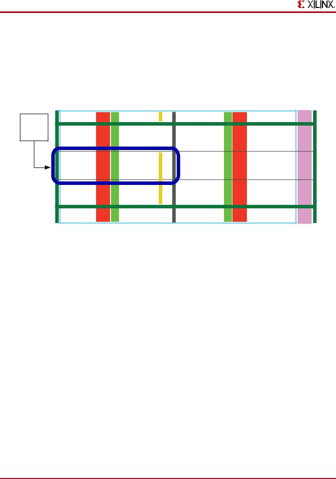
#LOCK
2EGION
8
Figure 3-8: SLR Showing Clock Regions (Enlarged)
The clocking architecture for SSI devices is similar to other Xilinx 7 series FPGA devices.
The regional clocking from the following components have the same connectivity and behavior as in Xilinx 7 series FPGA devices:
•BUFIO
•BUFR
•BUFH
Exception
There is a single exception.
For a BUFMR or BUFMRCE, the buffer does not span across SLR components.
If a BUFMR or BUFMRCE is located in the clock region of an SLR that directly borders a different SLR, then the following limitations apply:
1.The BUFMR or BUFMRCE can access only:
a.The clock region in which it is placed
b.The clock region directly adjacent in the same SLR
2.The BUFMR or BUFMRCE cannot access the adjacent SLR.
Xilinx recommends that you place a BUFMR or BUFMRCE in the center clock region of a given SLR. This gives it full access to span the clock regions above and below.
20 |
www.xilinx.com |
UG872 (v14.3) October 16, 2012 |

Clocking
It might not be necessary now to encapsulate all three clock regions for that particular clock domain. But doing so now gives you greater flexibility in providing the clock to all regions later on. Be sure to take this fact into account during clock and pin planning.
Global Clocking (BUFG)
Global clocking (BUFG) for SSI devices is also similar to other Xilinx 7 series FPGA devices.
•The global clocking topology is identical in the SLR.
•There are 32 available BUFG components that can span the entire device.
•Each BUFG component is capable of driving one of 12 horizontal clocks (BUFH) in a given clock region in the SLR.
For all SLR components in an SSI device (including clocking), make the same assumptions as for any other Xilinx 7 series FPGA device.
The BUFG components in an SLR can also clock synchronous elements in other SLR components. This is demonstrated by the connections and topology of the inter-SLR clocking. Each of the 32 BUFG components in an SLR drives one of 32 vertical tracks called the vertical global clocking line (also known as the global clocking backbone).
This connection traverses to the top and the bottom of the SLR for each BUFG, and allows connectivity to the horizontal row clocking.
At the boundary of the SLR, these vertical clocking spines connect to a very short interposer hop to connect the spine to the corresponding spine of the neighboring SLR.
This process drives the horizontal clocking resources of that SLR, and can continue up or down until all SLR components are connected. It creates a truly global clocking resource.
Because the vertical global clocking lines are a shared resource between the BUFG components of each SLR, some management of these resources might be required.
Large FPGA Methodology Guide |
www.xilinx.com |
21 |
UG872 (v14.3) October 16, 2012