

Chapter 3: Stacked Silicon Interconnect (SSI)
|
X |
X |
|
"5&' |
X |
|
X |
|
3,2 |
X |
X |
|
||
|
X |
X |
)NTERPOSER
|
X |
X |
3,2 |
"5&' |
X |
|
X |
|
|
X |
X |
|
X |
X |
8
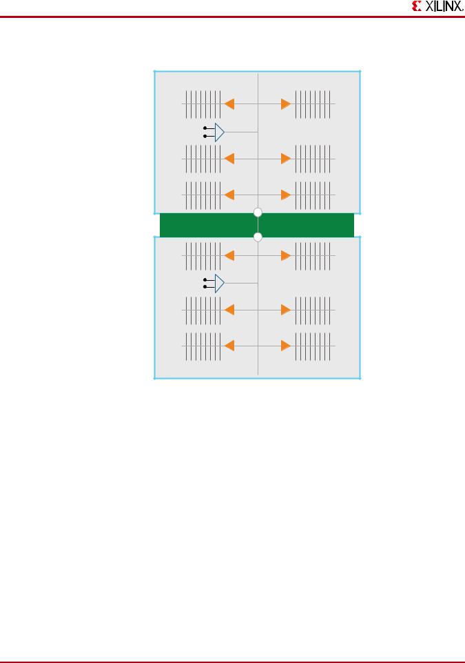
Figure 3-9: Global Clocking Connections in an SSI Device
The ratios and gap size between SLR components is for illustration purposes only. The actual gap is comparatively much smaller.
For more information, see Chapter 5, Clocking.
Management of Design Placement in SLR Components
This section discusses management of design placement in SLR components, and includes:
•Automatic SLR Assignment
•Manual SLR Assignment
Because SSI devices are composed of multiple SLR components, some management might be required. You must ensure that the design is properly placed in the device in order to route, function, and meet all timing goals.
22 |
www.xilinx.com |
UG872 (v14.3) October 16, 2012 |

Management of Design Placement in SLR Components
Automatic SLR Assignment
Xilinx tools have built-in algorithms to manage the placement of resources in an SSI device. The tools automatically attempt to fit a design into the SSI part, and select logic placement with SLR components.
Placement Strategies
Using the built-in placement algorithms, the tools attempt to:
1.Place the design in a way that does not exceed SLL resources.
2.Limit the number of timing critical paths that must cross SLR components.
3.Balance the resources in a way that does not overly fill an SLR with a given resource.
4.Limit the number of SLL crossings to a minimum.
By following these strategies, the tools try to strike a balance placement while meeting performance requirements.
Benefits of Limiting SLL Crossing
Limiting SLL crossing in general reduces power, and allows for more design growth without impacting inter-SLR connectivity.
Other Factors That Influence SLR Selection
Other design and implementation factors can also influence SLR selection. These factors include:
1.Pin placement
2.Clock selection
3.Resource type
4.Physical constraints such as floorplanning (PBlocks) and LOC constraints
5.Timing constraints
6.I/O Standards and other constraints
Xilinx recommends that you allow the tools to assign SLR components while making intelligent pin placement, clock selection, and other design choices.
Floorplanning
Floorplanning might be necessary for high performance portions of the design. Floorplan only when necessary.
Large FPGA Methodology Guide |
www.xilinx.com |
23 |
UG872 (v14.3) October 16, 2012

Chapter 3: Stacked Silicon Interconnect (SSI)
Manual SLR Assignment
Manual SLR assignment might be necessary when the tools do not find a solution that meets design requirements, or when run-to-run repeatability is important.
Performing Manual SLR Assignment
To perform manual SLR assignment:
1.Create large PBlocks (area groups).
2.Assign portions of the design to those area groups.
To assign large sections of the design to a single SLR:
1.Create a PBlock that encompasses a single SLR.
2.Assign the associated hierarchy of the logic to that PBlock.
While you can assign logic to multiple adjacent SLR components, you must ensure that the PBlock encompasses the entire SLR.
Do not create PBlocks that cross SLR boundaries without constraining the entire SLR. Doing so can it make it difficult for the automatic SLR placement algorithms to legalize placement.
Manual SLR Assignment Guidelines
When you manually assign logic to the SLR components, Xilinx recommends that you:
1.Place the design in a way that does not exceed SLL resources.
2.Limit the number of timing critical paths that must cross SLR components.
3.Balance the resources in a way that does not overly fill an SLR with a given resource.
4.Limit the number of SLL crossings to a minimum.
These guidelines are the same as the Placement Strategies followed in Automatic SLR Assignment. Following these guidelines makes it less likely that the assignments will violate present or future design rules.
For more information, see the Floorplanning Methodology Guide (UG633) cited in
Appendix A, Additional Resources.
SSI Hierarchy
A well defined hierarchy for an SSI design facilitates SLR assignment. Register the outputs of the hierarchical instances in order to ease the timing requirements if those signals must cross SLR components.
Follow this recommendation as well when using partitions for:
•Design reuse
•Team design
•Partial reconfiguration
Achieving High Performance Design in SSI Devices
Additional manual intervention might be required in order to achieve very high speed designs in SSI devices.
24 |
www.xilinx.com |
UG872 (v14.3) October 16, 2012 |