

Clock Skew in SSI Devices
"5&' |
|
"5&' |
X |
3,2 |
|
"5&' |
|
|
"5&' X |
|
3,2 |
"5&' |
X |
|
||
|
"5&' |
|
3,2 |
"5&' X |
|
"5&' |
|
"5&' |
|
8 |
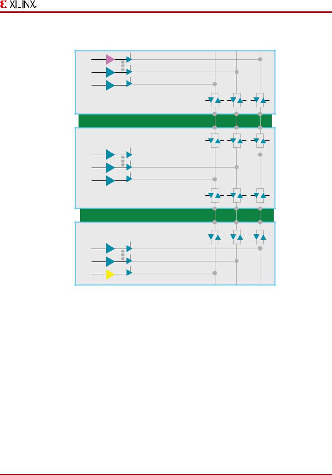
Figure 5-1: SSI Global Clocking Distribution and Shared Resources
Clock Skew in SSI Devices
Clock skew in a large FPGA device can represent a significant portion of the timing budget for a given path.
If left unmanaged and unchecked, excessive clock skew can create issues with:
•Maximum clock speed
•Hold times
SSI devices resemble other large FPGA devices in this respect. Skew is represented by:
•Unevenness in the distribution of the clock network from the source to destination.
•Small differences in process voltage and temperature (PVT) that can speed up or slow down portions of the clock path in respect to the data path.
Large FPGA Methodology Guide |
www.xilinx.com |
45 |
UG872 (v14.3) October 16, 2012

Chapter 5: Clocking
Multiple Die
Multiple die SLRs in a device exaggerate the process portion of the PVT equation.
Multiple die SLRs are managed by the Xilinx assembly process, in which only die of similar speed are ever packaged together.
Even with that extra action, the Xilinx timing tools account for these differences as a part of the timing report. During path analysis, the tools analyze these aspects as a part of the setup and hold calculations. The tools then report them as a part of the path delay against the specified requirements.
No additional calculations or considerations are necessary for SSI devices. The timing analysis tools take this into account.
Path Delay Differences
Path delay differences can also be exaggerated if you are using the top or bottom SLR. The difference to reach points farther away from each other might see more skew.
For this reason, Xilinx recommends placing global clocks that must drive more than one SLR into the center SLR. This allows a more even distribution of the clocking network across the part, generally resulting in less clock skew.
Specifying the Clocking in the Design
This section discusses Specifying the Clocking in the Design, and includes:
•Inference
•Synthesis Attributes
•Intellectual Property (IP)
•Instantiation
Inference
The synthesis tool automatically specifies a global buffer (BUFG) for any clock structures up to the maximum allowed in an architecture, unless otherwise specified or controlled by the synthesis tool.
The BUFG provides a well controlled, low skew network suitable for most clocking needs. Nothing more is required unless your design clocking exceeds the number or capabilities of BUFG components in the part.
Controlling the clocking structure can result in better characteristics with respect to factors such as:
•Jitter
•Skew
•Placement
•Power
•Performance
46 |
www.xilinx.com |
UG872 (v14.3) October 16, 2012 |

Clock Skew in SSI Devices
Synthesis Attributes
Using the proper synthesis attributes is a simple way to control clocking resources.
Uses of Synthesis Attributes
•Synthesis attributes can prevent BUFG inference.
•Synthesis attributes can replace a BUFG with an alternative clocking structure.
•Synthesis attributes can specify a clock buffer when one would not otherwise exist.
•Synthesis attributes can control clocking resources without modifying the HDL source code.
Using the BUFFER_TYPE Attribute in XST
You can use the BUFFER_TYPE attribute in the Xilinx Synthesis Technology (XST) tool to:
•Not specify a clocking buffer.
•Specify a specific buffer type such as BUFH or BUFR. The BUFFER_TYPE attribute can be placed:
•Directly in the HDL source code
This allows the constraint to persist in the code.
•In the XST Constraint File (XCF)
This allows you to control clocking resources without modifying the HDL source code.
Intellectual Property (IP)
Some intellectual property (IP) can help create clocking structures, including:
•Clocking Wizard and I/O Wizard
•Complex IP
Clocking Wizard and I/O Wizard
Clocking Wizard and I/O Wizard can help select and create clocking resources and structures, including:
•BUFG
•BUFIO
•BUFR
•Clock modifying blocks such as:
•Mixed Mode Clocking Manager (MMCM)
•I/O Phase Lock Loop (PLL)
Complex IP
Complex IP such as the following can also include clocking structures:
•Memory Interface Generator (MIG)
•PCIe
•Transceiver Wizard
This IP can provide additional clocking resources when properly taken into account.
Large FPGA Methodology Guide |
www.xilinx.com |
47 |
UG872 (v14.3) October 16, 2012

Chapter 5: Clocking
If not properly taken into account, this IP can limit some clocking options for the remainder of the design.
Xilinx recommends that, for any instantiated IP, you leverage the clocking requirements, capabilities, and resources in other portions of the design.
Instantiation
The most low level and direct method of controlling clocking structures is to instantiate the clocking resources into the HDL design.
•Benefits of Instantiation
•Instantiating Clocking Resources at the Top
•Dangers of Redundant Clocking Resources
Benefits of Instantiation
Instantiating the clocking resources into the HDL design allows you access and control all capabilities of the device.
Instantiation is generally the only option for clocking structures that require extra logic and control, including:
•BUFGCE
•BUFGMUX
•BUFHCE
Even for simple buffers, the quickest solution is to be direct and instantiate it into the design.
Instantiating Clocking Resources at the Top
Xilinx recommends placing the clocking resources in a separate entity or module at the top, or near the top, of the code.
An entity or module at or near the top level can be more easily distributed to multiple modules in the design.
Dangers of Redundant Clocking Resources
•Redundant clocking resources can waste FPGA resources.
•Redundant clocking resources can consume more power.
•Redundant clocking resources can create conflicts and placement decisions that result in:
•Longer implementation tool runtimes
•More complex timing scenarios
48 |
www.xilinx.com |
UG872 (v14.3) October 16, 2012 |